 Embedded HandbookApps
20а. USB OTG and host; 48 MHz without a crystal
Section 20 covered the microcontroller in the device role: enumeration, classes, the virtual COM port, the pull-up on D+ and 48 MHz from a crystal. Here — two other sides of USB. The first: the microcontroller itself becomes a host to which a flash drive or a keyboard is connected, and the OTG controller can switch roles. The second: how a device gets by without a crystal — HSI48 with CRS trimming on the host frames on the G4, and MSI locked to the watch crystal on the L476.
Sources: the reference manuals RM0090 (F4, chapter 34 "OTG_FS"), RM0440
(G4, chapter 8 "CRS" and the RCC chapter), RM0351 (L47x/L48x/L49x/L4Ax: MSI, CRS)
and the datasheets DS12288 (G474) and DS10198 (L476) from the Keil packs; the
stm32f4xx_ll_usb.c driver from the F4 pack; the ST USB Host library from the
STM32CubeF4 1.28.0 archive in the CubeMX repository; host examples from MDK-Middleware
8.1.0. The CRS and MSI calculations and the trimming model are on the PC, the code is built with armclang.
What it is called in the documentation
Original Meaning dual-role device (DRD) a controller with two roles: host and device A-device, B-device side A (supplies VBUS, host by default) and side B ID line the pin that tells which end of the cable is plugged in HNP, SRP negotiated role swap; session request to side A charge pump, power switch the 5 V source and the VBUS power switch overcurrent current overload host channel (pipe) a host channel start of frame (SOF) the start-of-frame packet, once every 1 ms clock recovery system (CRS) the block that trims HSI48 to an external reference RELOAD, FELIM the number of clocks between references and the error threshold TRIM the oscillator trimming code MSI PLL-mode (MSIPLLEN) MSI locked to the LSE watch crystal
20а.1 OTG roles: who is the host, who is the device
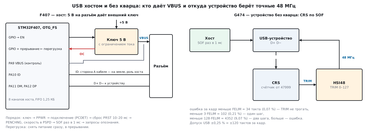
OTG_FS on the F407 is a dual-role controller (RM0090, 34.1). As a host it works at full (12 Mbit/s) and low (1.5 Mbit/s) speed, as a device — only at full speed. The role is set by the ID pin (PA10) when the cable is plugged into the micro-AB receptacle:
- the cable is plugged in with its B end, the ID wire is floating — the built-in pull-up sees a one, the device role (it is also the default);
- with its A end, where ID is shorted to ground — the
CIDSCHGinterrupt, and the controller switches to the host role by itself.
The FHMOD and FDMOD bits in OTG_FS_GUSBCFG lock the role: host only
or device only, and ID is then ignored. HNPCAP allows a negotiated role
swap (HNP), SRPCAP — the session request (SRP), in
which side A may turn VBUS off and turn it on on request.
One rule does not change: VBUS is always supplied by side A, whatever role
it plays at the moment (RM0090, 34.4.3).
OTG_FS pins on the F407: PA9 — VBUS sensing, PA10 — ID, PA11 and PA12 — DM and DP. The G474 has a different controller — device only (RM0440: "full-speed device interface"), the G4 is never a host. The L476 also has OTG_FS — with 12 host channels (20а.4).
20а.2 VBUS power: the switch and overload
A host must give the device 5 V, and the F407 does not generate it: "On-chip 5 V VBUS generation is not supported" (RM0090, 34.6). You need an external source — a boost converter or, if the board already has 5 V, a simple switch. In the RM0090 figures this is the STMPS2141 current-limited switch: the enable input is driven from any GPIO, the "overload" output goes to a GPIO with an interrupt.
The order from RM0090 (34.6.2):
- Turn the switch on with the GPIO pin and set the
PPWRbit inOTG_FS_HPRT. - On overload the interrupt handler immediately turns the switch off
and clears
PPWR. The controller itself also clearsPPWRif it sees an overload. - If HNP or SRP is enabled, PA9 is connected to VBUS: a drop below 4.25 V
gives the
SEDETinterrupt, and the power must be removed. Without HNP and SRP, PA9 is not connected to VBUS and is free as a GPIO.
void otg_host_port_power(int on)
{
    uint32_t h = OTG_HPRT & HPRT_KEEP;
    if (on) {
        vbus_switch(1);                             /* сначала сам ключ, потом бит PPWR */
        OTG_HPRT = h | USB_OTG_HPRT_PPWR;
    } else {
        OTG_HPRT = h & ~USB_OTG_HPRT_PPWR;
        vbus_switch(0);
    }
}
HPRT_KEEP removes four bits from the value read. PENA
can only be cleared by the program — and that disables the port; PCDET,
PENCHNG and POCCHNG are cleared by writing a one. Writing the register
back "as read" means disabling the port and losing events.
HAL does the same (USB_DriveVbus, USB_ResetPort).
The current budget is set in the stack: in MDK-Middleware it is USBH0_HC_POWER —
500 mA by default, from 2 to 500 allowed. The other side: if
a device on an STM32 is bus-powered, the 3.3 V regulator is fed from VBUS
(RM0090, note to 34.5).
20а.3 Device enumeration by the host
RM0090 (34.6.2) describes what the host does after a connection:
- The
PCDETinterrupt — a device is connected: its pull-up has appeared on DP (full speed) or DM (low speed). - Wait for
DBCDNE— the line has settled after the connection. - Bus reset: hold
PRSTfor 10 to 20 ms, then release it. - The
PENCHNGinterrupt, the speed is in thePSPDfield (01 — full, 10 — low). The host starts sending SOF once every millisecond. - Then come the enumeration requests on endpoint zero.
void otg_host_port_reset(void)
{
    uint32_t h = OTG_HPRT & HPRT_KEEP;
    OTG_HPRT = h | USB_OTG_HPRT_PRST;
    delay_ms(15u);
    OTG_HPRT = h & ~USB_OTG_HPRT_PRST;
}
The F4 HAL holds PRST for 100 ms and then waits another 10 (USB_ResetPort).
This does not contradict the bit description in RM0090: it gives a minimum of 10 ms, and
"the USB standard does not set an upper limit". But 34.6.2 says
"from 10 to 20 ms", and your own code had better stick to that.
The enumeration requests are in USBH_HandleEnum of the ST library (usbh_core.c):
| Step | Request | Why |
|---|---|---|
| 1 | GET_DESCRIPTOR (0x06), device, 8 bytes | learn bMaxPacketSize0 and reopen the endpoint 0 channels |
| 2 | GET_DESCRIPTOR, device, 18 bytes | VID, PID, string indices |
| 3 | SET_ADDRESS (0x05), address 1 | leave address 0; a 2 ms pause |
| 4 | GET_DESCRIPTOR, configuration, 9 bytes | learn wTotalLength |
| 5 | GET_DESCRIPTOR, full configuration | interfaces and endpoints |
| 6 | manufacturer, product, serial number strings | for the log |
| 7 | SET_CONFIGURATION (0x09) | the device is ready for work |
The library chooses the class by bInterfaceClass of the first interface.
A new device always starts at address 0, and the ST library always
gives it address 1 (USBH_DEVICE_ADDRESS). Steps 1, 2, 4 and 5 are retried
from a reset up to three times on error, then the library gives up and asks to
remove the device; a SET_ADDRESS error means immediate failure.
The delays in the library: 200 ms after connection, the reset (100 + 10 ms in HAL) and 100 ms after the reset — 410 ms before the first request.
20а.4 Host channels, MSC and HID
A host does not hold endpoints — it has channels. The OTG_FS of the F407 has 8
(RM0090, 34.6.3; USB_OTG_FS_HOST_MAX_CHANNEL_NBR = 8), the OTG_FS of the L476 —
12 (RM0351). Each channel is set up by the HCCHARx register for one
transfer: the device address, the endpoint number, the direction, the type,
the maximum packet, low speed. The controller does not run more transfers than it has channels
at once: the driver reallocates channels as they
become free. Hardware queues: up to 8 periodic requests (interrupt
and isochronous) and up to 8 non-periodic ones (control and bulk). The total
FIFO memory is 1.25 KB: a shared receive FIFO and two transmit FIFOs.
The control endpoint needs two channels — in and out (pipe_in,
pipe_out in the ST library). A flash drive needs two more on top of that for the bulk
endpoints: four of the eight channels are taken. In HAL a channel is opened by HAL_HCD_HC_Init (channel number, endpoint,
address, speed, type, maximum packet), and a transfer by HAL_HCD_HC_SubmitRequest.
The classes in brief:
| Class | Code | What is inside | MDK-Middleware |
|---|---|---|---|
| MSC, flash drive | 0x08 | Bulk-Only (0x50) + SCSI commands (0x06) | USBH_MSC_GetStatus, drive U0: via fmount |
| HID, keyboard and mouse | 0x03 | boot protocol: keyboard 0x01, mouse 0x02 | USBH_HID_GetKeyboardKey, USBH_HID_GetMouseState |
The codes are from usbh_msc.h and usbh_hid.h of the ST library. In MDK-Middleware
the host is started by USBH_Initialize(0), then the flash drive example polls
USBH_MSC_DriveGetMediaStatus("U0:") and writes a file with an ordinary fopen.
The host configuration template USBH_Config.h allows no more than 3 channels
at once (USBH0_HC_PIPE_NUM) and a memory pool of 640 bytes: no less than
the largest packet plus 128. The flash drive example takes
a pool of 4224 bytes.
20а.5 48 MHz accuracy and the CRS block
USB Full Speed requires 48 MHz with ±0.25 % accuracy (section 20.2). Over a 1 ms frame that is 48000 clocks and a tolerance of ±120 clocks.
HSI48 on the G474 after factory calibration is ±3 % at VDD 3.0–3.6 V and −15…85 °C, ±4.5 % over the full range (DS12288, table 44). That is 12 and 18 times worse than needed. So HSI48 does not work for USB on its own — it is trimmed by the CRS. The TRIM step per the datasheet is 0.11 % typical, 0.18 % maximum; RM0440 uses 0.14 % for calculations. On the G4 TRIM is 7 bits, 64 after reset (the middle); on the L4 — 6 bits, 32 after reset.
How the CRS works (RM0440, 8.4.3–8.4.4). On each SYNC event —
usually the SOF from the host — a 16-bit counter is loaded with RELOAD and
counts HSI48 clocks down to zero, then up. At the moment of the next
event its value is latched into FECAP, and the direction into FEDIR.
If the event came while the count was going down, the oscillator is slow and TRIM must be
increased; if it was going up, it is fast. Then the error is compared
with the thresholds:
| Error | Flag | Automatic trimming |
|---|---|---|
| less than FELIM | SYNCOK | TRIM does not change |
| from FELIM to 3·FELIM | SYNCOK | ±1 step |
| from 3·FELIM to 128·FELIM | SYNCWARN | ±2 steps |
| 128·FELIM and more | SYNCERR or SYNCMISS | TRIM does not change |
The formulas from RM0440 (8.4.5):
RELOAD = fTARGET / fSYNC − 1, FELIM = (fTARGET / fSYNC) × STEP / 100 % / 2, rounded up.
| Reference | fSYNC | RELOAD | FELIM at a 0.14 % step | CRS_CFGR |
|---|---|---|---|---|
| SOF | 1 kHz | 47999 (0xBB7F) | 33.6 → 34 (0x22) | 0x2022BB7F |
| LSE / 32 | 1024 Hz | 46874 (0xB71A) | 33 | 0x1521B71A |
For SOF the calculation gave exactly the reset value of CRS_CFGR — 0x2022BB7F:
SOF source, divider 1, FELIM 34, RELOAD 47999. RM0440 says as much:
the reset value is designed for 48 MHz, 1 kHz and a 0.14 % step. For the watch crystal
the divider 32 gives 1024 Hz, and 48 MHz divides by it exactly — 46875 clocks.
With a 0.11 % step FELIM would be 27, with 0.18 % — 44. The RM condition "RELOAD
greater than 128·FELIM" holds in all three cases: the largest
128·FELIM is 5632 against 47999.
In percent: FELIM of 34 clocks is 0.0708 %, 3·FELIM — 0.2125 %, 128·FELIM — 9.0667 %. A 0.14 % step is 67.2 clocks per frame.
20а.6 Trimming: model, code, MSI on the L476
Model on the PC. The HSI48 frequency depends linearly on TRIM, the initial error is from −3 to +3 % in 0.01 % steps (601 cases), and on each SOF the rule from the table above applies:
| Step | FELIM | TRIM oscillates | Time to settle, ms | Largest residual |
|---|---|---|---|---|
| 0.14 % | 34 | 0 of 601 | 11 | 0.07 % |
| 0.11 % | 27 | 0 of 601 | 14 | 0.05 % |
| 0.18 % | 44 | 0 of 601 | 9 | 0.09 % |
| 0.18 % | 34 | 102 of 601 | 9 | 0.10 % |
An example: with an error of +2.5 % and a 0.14 % step, TRIM goes 64 → 46 two steps per frame and settles in 9 ms; the residual is −0.02 %. The last row is the reset FELIM on a die with the largest step: the ±34-clock window is narrower than the 86.4-clock step, and in 102 cases out of 601 there is no suitable TRIM — the code jumps between two values every frame. It still fits within the tolerance (0.10 % against 0.25 %), but the model confirms the RM rule "FELIM is half the step".
G474 code. First HSI48 and selecting it for USB:
void usb_clock_hsi48(void)
{
    RCC->CRRCR |= RCC_CRRCR_HSI48ON;
    while (!(RCC->CRRCR & RCC_CRRCR_HSI48RDY)) {
    }
    RCC->CCIPR &= ~RCC_CCIPR_CLK48SEL;              /* 00: HSI48 → USB и RNG */
    RCC->APB1ENR1 |= RCC_APB1ENR1_CRSEN | RCC_APB1ENR1_USBEN;
}
Then the CRS. CRS_CFGR can be written only while CEN = 0: once the
counter is enabled, the register is locked.
void crs_start_sof(void)
{
    CRS->CFGR = CFGR_SOF;
    CRS->CR |= CRS_CR_AUTOTRIMEN | CRS_CR_CEN;
}
CFGR_SOF is computed by a macro from the RM0440 formulas, and a _Static_assert
in the file checks that it is 0x2022BB7F. armclang builds the function like this:
MOVW     r0,#0x2000
MOV      r1,#0xbb7f
MOVT     r0,#0x4000
MOVT     r1,#0x2022
STR      r1,[r0,#4]
LDR      r1,[r0,#0]
ORR      r1,r1,#0x60
STR      r1,[r0,#0]
BX       lr
0x2022BB7F goes into CRS_CFGR (0x4000 2004), then bits 6 and 5 (AUTOTRIMEN
and CEN, 0x60) into CRS_CR (0x4000 2000). The signed error of the last frame
in clocks is given by crs_error_ticks() from FECAP and FEDIR.
MSI in PLL mode on the L476. In the RM0351 line HSI48 exists only on the L49x
and L4Ax; the L476 does not have it. Instead, MSI at 48 MHz is locked to the LSE watch
crystal with the MSIPLLEN bit (RM0351, 6.2.3): "At 48 MHz, the MSI in
PLL-mode can be used for the USB OTG FS device". DS10198 gives 48.005 MHz typical in this
mode for range 11. The model — the nearest integer
multiple of 32768 Hz — matched table 60 of the datasheet in all 12
ranges. For 48 MHz: 48000000 / 32768 = 1464.84375 → 1465,
1465 × 32768 = 48005120 Hz, an error of +106.7 ppm = +0.0107 %. To this
the error of the watch crystal is added — according to the RM, usually
a few tens of ppm. The datasheet promises "better than ±0.25 %".
void usb_clock_msi_pll(void)
{
    RCC->APB1ENR1 |= RCC_APB1ENR1_PWREN;
    PWR->CR1 |= PWR_CR1_DBP;                        /* LSE живёт в домене резервного питания */
    RCC->BDCR |= RCC_BDCR_LSEON;
    while (!(RCC->BDCR & RCC_BDCR_LSERDY)) {
    }
    /* после сброса MSI — системный такт: сначала такты ожидания флеш-памяти */
    FLASH->ACR = (FLASH->ACR & ~FLASH_ACR_LATENCY) | FLASH_ACR_LATENCY_2WS;
    while ((FLASH->ACR & FLASH_ACR_LATENCY) != FLASH_ACR_LATENCY_2WS) {
    }
    while (!(RCC->CR & RCC_CR_MSIRDY)) {            /* MSIRANGE менять только при MSIRDY = 1 */
    }
    RCC->CR = (RCC->CR & ~RCC_CR_MSIRANGE) | RCC_CR_MSIRANGE_11 | RCC_CR_MSIRGSEL;
    RCC->CR |= RCC_CR_MSIPLLEN;                     /* только после LSERDY: иначе бит не встанет */
    RCC->CCIPR |= RCC_CCIPR_CLK48SEL;               /* 11: MSI → USB OTG FS */
}
48 MHz with the core voltage in range 1 requires 2 flash wait states (RM0351, table 11) — and MSI after reset is the system clock, so the latency is set before changing the range.
The documents promise both HSI48 with CRS and MSI from LSE only for a device.
A host has nothing to adjust to — it sends SOF itself, and its frame must
be accurate: at 48 MHz the F4 driver writes 48000 clocks per frame into HFIR.
A host needs a crystal (section 20.2).
20а.7 Pitfalls
The host port disabled itself after a write to HPRT. The register was written
back with the PENA = 1 that was read — that clears the bit, that is, disables
the port. Before writing, remove PENA, PCDET, PENCHNG, POCCHNG.
The flash drive is not seen, there is no 5 V on the connector. The F407 does not generate VBUS:
you need an external switch enabled by a GPIO, and the PPWR bit.
A short circuit in the device — and the switch or the regulator burns. The overload flag is not wired to an interrupt. Per RM0090 the handler turns the power off immediately.
The host does not see a connection with HNP or SRP enabled. In this mode RM0090 reports a connection only when VBUS is at a valid level: PA9 must be connected to VBUS.
CRS_CFGR does not change. It is written before CEN = 1 — after that the register
is protected. To change the source, clear CEN first.
CRS errors in LPM sleep. In LPM sleep the host does not send SOF, and
there is nothing to trim against; RM0440 advises taking the reference from LSE or an external
signal on a pin — that is crs_start_lse().
USB is silent after Stop. The HSI48ON bit is cleared by hardware on entering
Stop, the CRS registers freeze; after Standby the CRS must be configured again
(RM0440, 8.5). HSI48 is enabled again after wake-up.
No crystal in the cold. DS12288 allows crystal-less USB only from −15 to 85 °C.
MSIPLLEN does not set. LSE is not ready yet: the hardware protects the bit while
there is no LSERDY, and clears it if LSE is lost.
The L476 hangs when MSI switches to 48 MHz. The 2 flash wait states were not set before changing the range.
A host on HSI48 or MSI. It has nothing to adjust to — it needs a crystal.
20а.8 Summary
- OTG_FS on the F407 has two roles: ID pin grounded — host, floating — device;
FHMODandFDMODlock the role. VBUS is always supplied by side A. - A host on the F407 needs an external current-limited 5 V switch, the
PPWRbit, and the overload flag on an interrupt; the VBUS threshold with HNP and SRP is 4.25 V. - Enumeration: reset 10–20 ms, 8 bytes of the descriptor, 18 bytes, address 1, configuration 9 bytes and in full, SET_CONFIGURATION; in the ST library 410 ms of delays before the first request.
- The OTG_FS of the F407 has 8 host channels, the L476 — 12; the FIFO is 1.25 KB; MSC is class 0x08, HID — 0x03.
- The USB tolerance of ±0.25 % is ±120 clocks per frame; HSI48 on the G474 without trimming is
±3 %. CRS on SOF: RELOAD 47999, FELIM 34,
CRS_CFGR= 0x2022BB7F — the reset value; from LSE / 32 — 46874 and 33. - Model: from ±3 % the CRS reaches accuracy in 9–14 ms, the residual is 0.05–0.09 %; FELIM less than half a step — TRIM oscillates every frame.
- L476: MSI in PLL mode from LSE — 1465 × 32768 = 48005120 Hz, +0.0107 %.
- Without a crystal — device only; a host needs a crystal.
Full sources
usbh20a_f4.c — F407: the OTG_FS host port — VBUS power and bus reset.
/* 20а: F407 — порт хоста OTG_FS по регистрам: питание VBUS и сброс шины (RM0090, 34.6.2).
   Собирается armclang: -DSTM32F407xx -include stm32f4xx.h. */
#include <stdint.h>

#define OTG_HPRT    (*(volatile uint32_t *)(USB_OTG_FS_PERIPH_BASE + USB_OTG_HOST_PORT_BASE))
/* PENA программа может только сбросить (и выключить порт), три флага сбрасываются записью 1 */
#define HPRT_KEEP   (~(USB_OTG_HPRT_PENA | USB_OTG_HPRT_PCDET | USB_OTG_HPRT_PENCHNG | USB_OTG_HPRT_POCCHNG))

_Static_assert(USB_OTG_FS_HOST_MAX_CHANNEL_NBR == 8u, "у OTG_FS F407 восемь каналов хоста");
_Static_assert(USB_OTG_FS_PERIPH_BASE + USB_OTG_HOST_PORT_BASE == 0x50000440u, "OTG_FS_HPRT — 0x5000 0440");
_Static_assert(USB_OTG_HPRT_PPWR == (1u << 12) && USB_OTG_HPRT_PRST == (1u << 8), "PPWR — бит 12, PRST — бит 8");
_Static_assert(USB_OTG_GUSBCFG_FHMOD == (1u << 29), "FHMOD — только хост, вывод ID не смотрится");

extern void vbus_switch(int on);                    /* ключ 5 В с ограничением тока — выбранный GPIO */
extern void delay_ms(uint32_t ms);

void otg_host_port_power(int on)
{
    uint32_t h = OTG_HPRT & HPRT_KEEP;
    if (on) {
        vbus_switch(1);                             /* сначала сам ключ, потом бит PPWR */
        OTG_HPRT = h | USB_OTG_HPRT_PPWR;
    } else {
        OTG_HPRT = h & ~USB_OTG_HPRT_PPWR;
        vbus_switch(0);
    }
}

/* сброс шины: PRST держать от 10 до 20 мс; конец — прерывание PENCHNG, скорость в PSPD */
void otg_host_port_reset(void)
{
    uint32_t h = OTG_HPRT & HPRT_KEEP;
    OTG_HPRT = h | USB_OTG_HPRT_PRST;
    delay_ms(15u);
    OTG_HPRT = h & ~USB_OTG_HPRT_PRST;
}
usbh20a_g4.c — G474: USB without a crystal — HSI48 and CRS trimming on SOF.
/* 20а: G474 — USB-устройство без кварца: HSI48 и подстройка CRS по SOF (RM0440, глава 8).
   Собирается armclang: -DSTM32G474xx -include stm32g4xx.h. */
#include <stdint.h>

#define F_TARGET    48000000u               /* такт USB */
#define F_SOF       1000u                   /* SOF от хоста — раз в 1 мс */
#define STEP_X100   14u                     /* шаг TRIM 0,14 % — из RM0440, в сотых долях процента */

/* RM0440, 8.4.5: RELOAD = fTARGET / fSYNC − 1; FELIM = (fTARGET / fSYNC) · STEP / 100 % / 2, вверх */
#define CRS_RELOAD(fs)      (F_TARGET / (fs) - 1u)
#define CRS_FELIM(fs)       (((F_TARGET / (fs)) * STEP_X100 + 19999u) / 20000u)
#define CRS_CFGR_VAL(src, div, fs) \
    (((src) << CRS_CFGR_SYNCSRC_Pos) | ((div) << CRS_CFGR_SYNCDIV_Pos) \
     | (CRS_FELIM(fs) << CRS_CFGR_FELIM_Pos) | (CRS_RELOAD(fs) << CRS_CFGR_RELOAD_Pos))

#define SRC_LSE     1u                      /* SYNCSRC = 01 */
#define SRC_SOF     2u                      /* SYNCSRC = 10 */
#define DIV_32      5u                      /* SYNCDIV = 101: 32 768 / 32 = 1024 Гц */
#define F_LSE_32    (32768u / 32u)

#define CFGR_SOF    CRS_CFGR_VAL(SRC_SOF, 0u, F_SOF)
#define CFGR_LSE    CRS_CFGR_VAL(SRC_LSE, DIV_32, F_LSE_32)

_Static_assert(CRS_RELOAD(F_SOF) == 47999u, "RELOAD для SOF — 47999 (0xBB7F)");
_Static_assert(CRS_FELIM(F_SOF) == 34u, "FELIM: 48000 · 0,14 % / 2 = 33,6 → 34");
_Static_assert(CFGR_SOF == 0x2022BB7Fu, "для 48 МГц и SOF CRS_CFGR совпадает со значением после сброса");
_Static_assert(CRS_RELOAD(F_SOF) > 128u * CRS_FELIM(F_SOF), "RELOAD больше OUTRANGE = 128 · FELIM");
_Static_assert(F_TARGET % F_LSE_32 == 0u, "48 МГц делится на 1024 Гц нацело: 46875 тактов");
_Static_assert(CFGR_LSE == 0x1521B71Au, "LSE / 32: RELOAD 46874, FELIM 33");
_Static_assert(CRS_CR_TRIM_Msk == (0x7Fu << 8), "у G4 TRIM — 7 бит (у L4 — 6)");
_Static_assert(RCC_CCIPR_CLK48SEL_Pos == 26u, "CLK48SEL — биты 27:26, 00 — HSI48");

/* включить HSI48 и отдать его USB */
void usb_clock_hsi48(void)
{
    RCC->CRRCR |= RCC_CRRCR_HSI48ON;
    while (!(RCC->CRRCR & RCC_CRRCR_HSI48RDY)) {
    }
    RCC->CCIPR &= ~RCC_CCIPR_CLK48SEL;              /* 00: HSI48 → USB и RNG */
    RCC->APB1ENR1 |= RCC_APB1ENR1_CRSEN | RCC_APB1ENR1_USBEN;
}

/* подстройка по SOF: CFGR пишется только при CEN = 0, потом он закрыт */
void crs_start_sof(void)
{
    CRS->CFGR = CFGR_SOF;
    CRS->CR |= CRS_CR_AUTOTRIMEN | CRS_CR_CEN;
}

/* подстройка по часовому кварцу LSE / 32 — когда SOF нет (сон LPM, нет хоста) */
void crs_start_lse(void)
{
    CRS->CR &= ~CRS_CR_CEN;
    CRS->CFGR = CFGR_LSE;
    CRS->CR |= CRS_CR_AUTOTRIMEN | CRS_CR_CEN;
}

/* ошибка последнего кадра в тактах HSI48: плюс — частота выше 48 МГц */
int32_t crs_error_ticks(void)
{
    uint32_t isr = CRS->ISR;
    int32_t fecap = (int32_t)((isr & CRS_ISR_FECAP_Msk) >> CRS_ISR_FECAP_Pos);
    return (isr & CRS_ISR_FEDIR) ? -fecap : fecap;  /* FEDIR = 1: счёт вниз, частота ниже */
}
usbh20a_l4.c — L476: MSI 48 MHz in PLL mode from LSE.
/* 20а: L476 — USB без кварца 8 МГц: MSI 48 МГц в режиме PLL от LSE (RM0351, 6.2.3).
   Собирается armclang: -DSTM32L476xx -include stm32l4xx.h. */
#include <stdint.h>

_Static_assert(RCC_CR_MSIRANGE_11 == (0xBu << RCC_CR_MSIRANGE_Pos), "диапазон 11 — около 48 МГц");
_Static_assert(RCC_CR_MSIPLLEN == (1u << 2), "MSIPLLEN — бит 2 RCC_CR");
_Static_assert(RCC_CCIPR_CLK48SEL == (3u << 26), "CLK48SEL = 11 — MSI для USB OTG FS");
_Static_assert(FLASH_ACR_LATENCY_2WS == 2u, "48 МГц в диапазоне 1 — 2 такта ожидания");

void usb_clock_msi_pll(void)
{
    RCC->APB1ENR1 |= RCC_APB1ENR1_PWREN;
    PWR->CR1 |= PWR_CR1_DBP;                        /* LSE живёт в домене резервного питания */
    RCC->BDCR |= RCC_BDCR_LSEON;
    while (!(RCC->BDCR & RCC_BDCR_LSERDY)) {
    }
    /* после сброса MSI — системный такт: сначала такты ожидания флеш-памяти */
    FLASH->ACR = (FLASH->ACR & ~FLASH_ACR_LATENCY) | FLASH_ACR_LATENCY_2WS;
    while ((FLASH->ACR & FLASH_ACR_LATENCY) != FLASH_ACR_LATENCY_2WS) {
    }
    while (!(RCC->CR & RCC_CR_MSIRDY)) {            /* MSIRANGE менять только при MSIRDY = 1 */
    }
    RCC->CR = (RCC->CR & ~RCC_CR_MSIRANGE) | RCC_CR_MSIRANGE_11 | RCC_CR_MSIRGSEL;
    RCC->CR |= RCC_CR_MSIPLLEN;                     /* только после LSERDY: иначе бит не встанет */
    RCC->CCIPR |= RCC_CCIPR_CLK48SEL;               /* 11: MSI → USB OTG FS */
}
Next: section 20б "USB-C and UCPD: power and roles over the cable" — how a USB-C connector negotiates by itself who is the host and who supplies power, and how the G474 does this with the UCPD block.