 Embedded HandbookApps
20б. USB-C and UCPD: power and roles over the cable
Section 20 covered the USB device: the D+ and D− lines, the 48 MHz clock, the pull-up, the classes. Section 20а covered the host and OTG. The Type-C connector has two more lines, CC1 and CC2, and no data travels over them. Over them the source and the sink recognize each other, find out which way round the cable is plugged in and how much current may be drawn. On top of the same line runs the Power Delivery protocol: through it the sides agree on a voltage above 5 V. The G0 and G4 have the UCPD block for this. Here — the resistors on CC, the "dead battery" and its pins, the Power Delivery frame (a model on the PC), the UCPD dividers and the code of a sink at register level.
Sources: the reference manuals RM0440 (G4, chapter 46 UCPD) and RM0444 (G0,
chapter 38), the STM32G474 (DS12288) and STM32G071 (DS12232) datasheets from the Keil
packs, the LL UCPD driver from the G4 pack, the USBPD_Analyzer example for the
STM32G071B-DISCO board and the STM32_USBPD_Library library from the
STM32Cube_FW_G0 V1.6.0 package. The USB Type-C and Power Delivery standards themselves are not
on disk, so the Rp values and the voltage thresholds on CC are not given here:
the ST documents do not quote them.
What it is called in the documentation
Original Meaning CC, configuration channel the configuration line: CC1 and CC2 in the connector Rp, Rd, Ra the source pull-up to supply; the sink pull-down to ground; the load of a cable powered by VCONN source, sink, DRP source, sink, dual-role port dead battery Rd is present even on an unpowered chip VCONN power for the cable electronics over the free CC line USB Power Delivery (PD) the protocol for agreeing on voltage and current over the CC line BMC, bi-phase mark coding biphase coding: a transition at every bit boundary 4b5b, K-code the "4 bits → 5 bits" code; a K-code is a special five-bit symbol ordered set, SOP, EOP an ordered set of four K-codes; start and end of packet PDO, Source_Capabilities a power data object; the source's "what I can do" message hbit_clk the half-bit clock tTransitionWindow, tInterFrameGap the window for checking line idle; the gap between frames
20б.1 The CC lines: who is the source, who is the sink
The Type-C connector has two configuration lines, CC1 and CC2, while the cable has a single CC wire. Which of the two lines it lands on depends on which way round the plug was inserted. The source pulls both its lines up to the supply with Rp resistors, the sink pulls both its lines down to ground with Rd resistors. Through the cable Rp and Rd meet on only one line, and this forms a divider:
- the source sees Rd on one of the lines — a sink is connected, and the line number tells the cable orientation;
- the sink sees the divider voltage, and from its level learns what current the source allows: the default current, 1.5 A or 3 A. Which one is chosen by the source through the Rp value;
- there is only one CC wire, so the sink's second line is free. A cable with its own electronics puts Ra on it and asks for VCONN power.
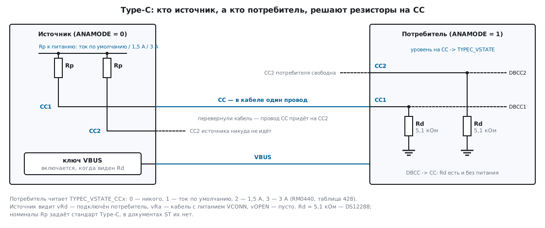
The built-in Rd of the UCPD is 5.1 kΩ (DS12288, note to the pin table;
RM0440, the section on debug pins). The UCPD also has built-in Rp, "of all
values", selected by the ANASUBMODE field. The role is set by the ANAMODE bit
of the UCPD_CR register: 0 — source, 1 — sink. The UCPD puts the level on each
line after the debounce filter into the TYPEC_VSTATE_CC1 and
TYPEC_VSTATE_CC2 fields of the UCPD_SR register. What their values mean depends
on the role (table 428 of RM0440, table 237 of RM0444):
Role, ANASUBMODE |
0 | 1 | 2 | 3 |
|---|---|---|---|---|
| source, 01 — default current | vRa | vRd | vOPEN | — |
| source, 10 — 1.5 A | vRa | vRd | vOPEN | — |
| source, 11 — 3 A | vRa | vRd | vOPEN | — |
| sink | vRa | vRd-USB | vRd-1.5 | vRd-3.0 |
For a source TYPEC_VSTATE = 1 means "a sink is present", 0 — "a cable with
Ra", 2 — "nothing". For a sink 1, 2 and 3 mean the default current, 1.5 A and 3 A,
and 0 means there is no source; in LL this value is called
LL_UCPD_SNK_CCx_VOPEN. To change the allowed current on the fly,
the source simply rewrites ANASUBMODE, and on the sink side
the TYPECEVT event fires and TYPEC_VSTATE changes.
A sink that is happy with 5 V and the default current does not need UCPD: the source only needs Rd on CC. UCPD is needed when you have to know the allowed current or the cable orientation, or negotiate over Power Delivery.
UCPD controls neither the VBUS switch nor the VCONN switch (note to table
428): on a source they are driven by the program according to the CC state. The example in
table 429 of RM0440: a 3 A source sees Rd on CC1, waits in the
AttachWait state for 100–200 ms, sees Ra on CC2 — applies VCONN there with an external
switch and disconnects CC2 from its block with the CCENABLE field.
20б.2 Dead battery: which pins to connect
A device with a discharged battery is powered only from USB-C. But the source will not apply VBUS until it sees Rd, and a microcontroller without power cannot enable Rd. That is why the UCPD has a "dead battery" Rd: it is connected to CC while the chip is unpowered, if a high level arrives on the DBCC pin. For this, on the board DBCC1 is connected to CC1 and DBCC2 to CC2. For a device that does not need this (source only), the RM says to tie both DBCC pins to ground.
| STM32G474, UCPD1 | STM32G071, UCPD1 | |
|---|---|---|
| CC1 | PB6 | PA8 |
| CC2 | PB4 (also NJTRST) | PB15 |
| DBCC1 | PA9 | PA9 |
| DBCC2 | PA10 | PA10 |
| remove the dead battery Rd | PWR_CR3.UCPD1_DBDIS (bit 14) |
strobe SYSCFG_CFGR1.UCPD1_STROBE (bit 9) |
On the G071, in some small packages the DBCC role belongs to PC6 and PB0, and the second UCPD2 block is on PD0–PD3 (table 12 of DS12232). If DBCC is connected to CC, then PA9 and PA10 hang on the CC lines, and USART1 or I2C1 can no longer be placed on them.
After reset the dead battery Rd is enabled by itself — by the level on DBCC. It is disabled like this:
- G4. First configure the UCPD (
ANAMODE,ANASUBMODE), then setUCPD1_DBDISinPWR_CR3: the dead battery Rd then goes away and what has been configured starts working. RM0440 advises setting this bit always — both when UCPD is not needed and when it is. - G0. First configure the UCPD, then write 1 to
UCPD1_STROBE: the strobe applies the configuration to the pins. If UCPD is disabled, the same strobe simply removes the pull-down. A program that does not need UCPD issues the strobe at startup (note 3 to the pin table of DS12232).
In Standby UCPD does not work, but the configured pull resistors remain; without power the dead battery Rd remains (table 430 of RM0440). The supply of the UCPD itself per the datasheets: sink only — 3.0–3.6 V, source and sink — 3.135–3.465 V.
20б.3 The Power Delivery frame: what UCPD adds
A Power Delivery message goes over the same CC line that carries the cable wire. The frame (figure 677 of RM0440):
| Part | Who supplies it | 4b5b |
|---|---|---|
| preamble — receiver lock-in | UCPD | no |
| SOP — four K-codes | UCPD, from UCPD_TX_ORDSET |
yes |
| header, 2 bytes | the program | yes |
| data objects of 4 bytes | the program | yes |
| CRC-32 | UCPD | yes |
| EOP — one K-code | UCPD | yes |
Every 4 data bits are replaced with a five-bit code (table 424):
| 4 bits | 0 | 1 | 2 | 3 | 4 | 5 | 6 | 7 |
|---|---|---|---|---|---|---|---|---|
| 5 bits | 11110 | 01001 | 10100 | 10101 | 01010 | 01011 | 01110 | 01111 |
| 4 bits | 8 | 9 | A | B | C | D | E | F |
| 5 bits | 10010 | 10011 | 10110 | 10111 | 11010 | 11011 | 11100 | 11101 |
Special K-codes: Sync-1 — 11000, Sync-2 — 10001, Sync-3 — 00110, RST-1 — 00111, RST-2 — 11001, EOP — 01101. The five code bits are written from b4 to b0, and b0 goes onto the line first; for a byte the low nibble goes first (figures 675 and 676).
Four K-codes make up an ordered set (table 425):
| Set | K-code 1 | K-code 2 | K-code 3 | K-code 4 |
|---|---|---|---|---|
| SOP | Sync-1 | Sync-1 | Sync-1 | Sync-2 |
| SOP’ | Sync-1 | Sync-1 | Sync-3 | Sync-3 |
| SOP’’ | Sync-1 | Sync-3 | Sync-1 | Sync-3 |
| Hard Reset | RST-1 | RST-1 | RST-1 | RST-2 |
| Cable Reset | RST-1 | Sync-1 | RST-1 | Sync-3 |
Which sets to catch is set for the receiver by the RXORDSETEN bits in UCPD_CFG1
(bit 0 — SOP). Hard Reset interrupts even a transmission in progress: UCPD
cuts it off with the EOP code and sends the reset (the TXHRST bit). The receiver accepts
a set if any three of the four K-codes are correct.
CRC-32 uses the same polynomial 0x04C11DB7 as the CRC block (RM0440, the
CRC chapter). The receiver runs both the data and the CRC itself through the CRC register and at the end
compares the register with a constant residue: if it matches — RXMSGEND, if not —
RXERR as well.
On top of 4b5b the bits go out in BMC code: the level changes at every bit boundary, and for a one also in the middle. Such a signal does not depend on polarity and carries almost no DC component, and the receiver recovers the frequency from the preamble.
20б.4 Model on the PC: Source_Capabilities bit by bit
The model _verify/ucpd20b/ucpd20b.py does what UCPD does
in hardware: it assembles the message, computes the CRC, encodes 4b5b and BMC, then
decodes it back. The message is Source_Capabilities with a single object:
fixed 5 V and 3 A.
- Header 0x11A1: message type 1 (Source_Capabilities), data role
DFP, revision 3.0, power role — source, message number 0, one
data object. The field layout is from
demo_disco.c(USBPD_Analyzer), the values fromusbpd_def.h. - Object 0x0001912C: type "fixed supply", voltage 100 × 50 mV,
current 300 × 10 mA (the
USBPD_PDO_SRC_FIXED_*fields inusbpd_def.h). - The program writes 6 bytes into the transmitter:
A1 11 2C 91 01 00, which isTX_PAYSZ= 6.
The CRC of these six bytes is 0x312C2EDA; zlib.crc32 and a shift register with the
polynomial 0x04C11DB7 give the same result. After the data and the CRC the register
holds 0xC704DD7B — for this message and for three others. RM0440 and
RM0444 print 0xC704DD78: the difference is in the two low bits. zlib on the same
frame leaves 0xDEBB20E3, which is 0xC704DD7B with the bits in reverse
order. It looks like a typo in the RM. The program does not need the residue: the
UCPD checks it and reports the result with the RXERR flag.
The frame after the preamble: SOP 20 bits + data 60 + CRC 40 + EOP 5 = 125 bits.
Of the 5 code bits, 4 are payload — 80 %. At 285.7 kbit/s (default
dividers, 20б.5) the frame without the preamble takes 437.5 µs. The first 20 bits on the
line, the SOP: 00011000110001110001.
The BMC encoder in the model:
def bmc(bits, level=0):                    # переход на каждой границе бита, для 1 — ещё в середине
    out = []
    for b in bits:
        level ^= 1
        out.append(level)
        if b:
            level ^= 1
        out.append(level)
    return out
125 bits give 250 half-bits. There are 66 ones, 59 zeros, 191 transitions = 125 boundaries + 66 middles; the sum of the half-bits (+1 and −1) is 2, that is, there is almost no DC component. The reverse parsing — BMC, 5 bits, 4 bits — finds the SOP and EOP, the header 0x11A1, the object 0x0001912C and the same CRC residue. An inverted signal decodes the same way. One corrupted bit in the object gives the residue 0x0F202F54 — the message is discarded. An SOP with one corrupted K-code is accepted, with two it is not.
20б.5 Dividers: 300 kbit/s from HSI16
UCPD is clocked from HSI16 (ucpd_ker_ck) and divides it three times
(figure 674 of RM0440):
PSC_USBPDCLK— a prescaler /1, /2, /4, /8, /16 →ucpd_clk. The RM advises keepingucpd_clkwithin 6–9 MHz;HBITCLKDIV— dividesucpd_clkby the field value plus one (1…64) →hbit_clk, the half-bit clock, about 600 kHz; a bit is two half-bits, hence about 300 kbit/s;TRANSWIN— the window for checking idle before transmission, in half-bits (field plus one, 0x09 — 10 recommended); the window must be 12–20 µs. The line is idle if there are fewer than three transitions in the window;IFRGAP— a divider ofucpd_clkfor the gap between frames (field plus one); per the RM, 15 — for the nominal frequency.
All four fields are in UCPD_CFG1, and they can be written only while UCPDEN = 0.
What each prescaler gives:
PSC_USBPDCLK |
ucpd_clk |
within 6–9 MHz | divider closest to 600 kHz | hbit_clk |
bit |
|---|---|---|---|---|---|
| /1 | 16.0 MHz | no | /27 | 592.6 kHz | 296.3 kbit/s |
| /2 | 8.0 MHz | yes | /13 | 615.4 kHz | 307.7 kbit/s |
| /4 | 4.0 MHz | no | /7 | 571.4 kHz | 285.7 kbit/s |
| /8 | 2.0 MHz | no | /3 | 666.7 kHz | 333.3 kbit/s |
| /16 | 1.0 MHz | no | /2 | 500.0 kHz | 250.0 kbit/s |
Only /2 falls into the recommended band. LL_UCPD_StructInit does exactly
that: /2 → 8.0 MHz, HBITCLKDIV = 0x0D (/14) → 571.4 kHz, bit
285.7 kbit/s, half-bit 1.750 µs, bit 3.500 µs. TRANSWIN = 0x7 — 8
half-bits, 14.0 µs; the RM-recommended 0x09 would give 17.5 µs; both are within
12–20 µs. IFRGAP = 0x10 — division by 17. The register gets
UCPD_CFG1 = 0x23C0D, and with SOP reception enabled (RXORDSETEN, bit 0) —
0x123C0D. The RM example HBITCLKDIV = 0x1A (/27) is designed for a ucpd_clk
of 16 MHz without a prescaler: 592.6 kHz and 296.3 kbit/s. /13 at 8 MHz would give
615.4 kHz — closer to 600, but above it; the speed tolerance is set by the PD standard,
which is not on disk, so there will be no "suitable or not" verdict here.
The USBPD_Analyzer example for the STM32G071B-DISCO board and the
STM32_USBPD_Library library use the same LL_UCPD_StructInit.
20б.6 Code: a sink at register level
The file _verify/ucpd20b/ucpd20b.c is built by armclang for the STM32G474 and
STM32G071. Sink setup:
void ucpd_sink_init(void)
{
#if defined(STM32G474xx)
    RCC->AHB2ENR  |= RCC_AHB2ENR_GPIOBEN;
    RCC->APB1ENR1 |= RCC_APB1ENR1_PWREN;
    RCC->APB1ENR2 |= RCC_APB1ENR2_UCPD1EN;
    GPIOB->PUPDR &= ~GPIO_PUPDR_PUPD4;                        /* PB4 после сброса — NJTRST с подтяжкой */
    GPIOB->MODER |= GPIO_MODER_MODE4 | GPIO_MODER_MODE6;      /* CC2 = PB4, CC1 = PB6 — аналоговый режим */
#elif defined(STM32G071xx)
    RCC->IOPENR  |= RCC_IOPENR_GPIOAEN | RCC_IOPENR_GPIOBEN;
    RCC->APBENR2 |= RCC_APBENR2_SYSCFGEN;
    RCC->APBENR1 |= RCC_APBENR1_UCPD1EN;
    GPIOA->MODER |= GPIO_MODER_MODE8;                         /* CC1 = PA8 */
    GPIOB->MODER |= GPIO_MODER_MODE15;                        /* CC2 = PB15 */
#endif
    UCPD1->CFG1 = UCPD_CFG1_DIVS | UCPD_CFG1_RXORDSETEN_0;   /* пишется только при UCPDEN = 0; приём SOP */
    UCPD1->CFG1 |= UCPD_CFG1_UCPDEN;
    UCPD1->CR = UCPD_CR_ANAMODE | UCPD_CR_CCENABLE;          /* пишется только при UCPDEN = 1 */
#if defined(STM32G474xx)
    PWR->CR3 |= PWR_CR3_UCPD_DBDIS;                          /* Rd мёртвой батареи — долой, дальше Rd от UCPD */
#elif defined(STM32G071xx)
    SYSCFG->CFGR1 |= SYSCFG_CFGR1_UCPD1_STROBE;              /* строб: применить ANAMODE к выводам */
#endif
}
The order here is not accidental: UCPD_CFG1 can be written only with the block
disabled, UCPD_CR only with it enabled, and the dead battery Rd is removed
after the role has been set. Disabling the block (UCPDEN = 0) resets
all control bits — after that the setup is repeated. The _Static_asserts
in the file check against the CMSIS headers the UCPD1 address (0x4000A000), the value
UCPD_CFG1 = 0x23C0D, the position of the TYPEC_VSTATE fields (bits 16 and 18),
ANAMODE | CCENABLE = 0xE00 and the UCPD1_DBDIS and UCPD1_STROBE bits.
Polling the lines:
int ucpd_sink_poll(unsigned *cc2)
{
    uint32_t sr = UCPD1->SR;
    uint32_t v1 = (sr & UCPD_SR_TYPEC_VSTATE_CC1) >> UCPD_SR_TYPEC_VSTATE_CC1_Pos;
    uint32_t v2 = (sr & UCPD_SR_TYPEC_VSTATE_CC2) >> UCPD_SR_TYPEC_VSTATE_CC2_Pos;

    if (v1 != CC_OPEN && v2 == CC_OPEN) { *cc2 = 0; return (int)v1; }
    if (v1 == CC_OPEN && v2 != CC_OPEN) { *cc2 = 1; return (int)v2; }
    return CC_OPEN;                                         /* обе открыты — никого; обе заняты — не кабель */
}
For the G474, armclang with -O2 turns it into 18 instructions — one read of
UCPD1->SR at address 0x4000 A014 and two UBFX field extractions:
MOV      r1,#0xa014
MOVT     r1,#0x4000
LDR      r2,[r1,#0]
UBFX     r1,r2,#16,#2
UBFX     r2,r2,#18,#2
CBZ      r1,{pc}+0x8 ; 0x1a
CBNZ     r2,{pc}+0x6 ; 0x1a
MOVS     r3,#0
B        {pc}+0x10 ; 0x28
CMP      r1,#0
MOV      r1,#0
BNE      {pc}+0xa ; 0x2a
CBZ      r2,{pc}+0x8 ; 0x2a
MOVS     r3,#1
MOV      r1,r2
STR      r3,[r0,#0]
MOV      r0,r1
BX       lr
Once a source is found, ucpd_sink_attach sets PHYCCSEL to its line and
enables the PHYRXEN receiver. Attach stability (how long to hold the
level before trusting it) is set by the Type-C standard; UCPD itself
filters out only bounce and spikes. Sending a message:
int ucpd_send(const uint8_t *msg, unsigned len)
{
    unsigned i = 0;
    uint32_t sr;

    UCPD1->TX_ORDSET = PD_SOP;
    UCPD1->TX_PAYSZ = len;                                  /* с заголовком, без CRC */
    UCPD1->CR |= UCPD_CR_TXSEND;                            /* TXMODE = 0: обычное сообщение */
    do {
        sr = UCPD1->SR;
        if ((sr & UCPD_SR_TXIS) && i < len)
            UCPD1->TXDR = msg[i++];                         /* TXIS: регистр пуст, следующий байт */
    } while (!(sr & (UCPD_SR_TXMSGSENT | UCPD_SR_TXMSGDISC)));
    UCPD1->ICR = UCPD_ICR_TXMSGSENTCF | UCPD_ICR_TXMSGDISCCF;
    return (sr & UCPD_SR_TXMSGSENT) ? 0 : -1;
}
PD_SOP = 0x8E318 — four K-codes of 5 bits, the first in the low bits,
as the TX_ORDSET description requires; LL_UCPD_ORDERED_SET_SOP gives the same
value. For the message from 20б.4 len = 6. UCPD itself
adds the preamble, the CRC and the EOP. TXMSGDISC means the transmission
was discarded: a reception is in progress on the line or there is strong interference. This is only
the physical layer. The Power Delivery protocol — acknowledgements, timers,
the voltage request — is done by STM32_USBPD_Library.
20б.7 Pitfalls
On the G474 JTAG does not connect, PB4 has a foreign level. PB4 is both
NJTRST and CC2. After reset the 5.1 kΩ dead battery Rd may hang on it —
it is enabled by a high level on PA10 (DBCC2). For JTAG RM0440
requires setting UCPD1_DBDIS.
G071: PA8 or PB15 is pulled to ground although UCPD is not used. The dead battery
Rd is enabled after reset. You need the UCPD1_STROBE strobe at
startup.
The UCPD setup has no effect. UCPD_CFG1 can be written only while
UCPDEN = 0, UCPD_CR only while UCPDEN = 1. A write at the wrong time
is silently lost.
The role is set, but CC still has Rd. On the G4 until
UCPD1_DBDIS is set, on the G0 until the strobe has been issued, the dead battery Rd is in effect,
not the configuration.
Without power the device does not charge from USB-C. DBCC1 and DBCC2 are not connected to CC1 and CC2 — there is no dead battery Rd, the source does not see the sink and does not supply VBUS.
The source outputs VBUS when nobody is connected. UCPD does not control the VBUS switch. The program must turn it on only on vRd on one of the lines.
UCPD at 3.0 V does not work as a source. Source plus sink together need 3.135–3.465 V; from 3.0 V — sink only.
Your own CRC check does not match the number from the RM. The RM prints the residue
0xC704DD78, the model and zlib give 0xC704DD7B. There is no need to check the CRC manually
— UCPD does it and sets RXERR.
20б.8 Summary
- The source pulls CC up through Rp, the sink down through Rd
(5.1 kΩ on the UCPD); the line with Rd shows the orientation, the level shows the current:
TYPEC_VSTATE1, 2, 3 — the default current, 1.5 A and 3 A. - Dead battery: DBCC1 → CC1, DBCC2 → CC2 on the board; it is removed after
setting the role —
PWR_CR3.UCPD1_DBDIS(G4) or the strobeSYSCFG_CFGR1.UCPD1_STROBE(G0). On the G474 CC2 is PB4/NJTRST. - Frame: preamble, SOP (4 K-codes, 20 bits), header and data in 4b5b, CRC-32 with the polynomial 0x04C11DB7, EOP; BMC on top.
- Source_Capabilities 5 V 3 A: 6 bytes, 125 bits, 250 half-bits, 437.5 µs; CRC 0x312C2EDA, residue 0xC704DD7B (in the RM — 0xC704DD78).
- Default dividers: HSI16 / 2 = 8 MHz, / 14 = 571.4 kHz per half-bit,
285.7 kbit/s; window 14 µs;
UCPD_CFG1= 0x23C0D.
Full sources
ucpd20b.py — a model of the Power Delivery physical layer on the PC.
# -*- coding: utf-8 -*-
"""Раздел 20б: модель физического уровня USB Power Delivery на ПК — то, что UCPD делает
аппаратно. Собирает сообщение Source_Capabilities, считает CRC-32, кодирует 4b5b и BMC,
декодирует обратно и сверяет остаток CRC; плюс расчёт делителей UCPD из RM0440.

Опоры (все на диске):
  RM0440, глава 46 (G4) и RM0444, глава 38 (G0): таблица 424 4b5b, таблица 425 ordered sets,
    таблица 426 «три K-кода из четырёх», таблица 427 размеры, рис. 676 порядок битов,
    остаток CRC, CFG1: PSC_USBPDCLK, HBITCLKDIV, TRANSWIN, IFRGAP;
  RM0440, глава CRC: многочлен CRC-32 (Ethernet) 0x4C11DB7;
  stm32g4xx_ll_ucpd.c: LL_UCPD_StructInit (PSC /2, HBITCLKDIV 0x0D, TRANSWIN 0x7, IFRGAP 0x10);
  stm32g4xx_ll_ucpd.h: LL_UCPD_SYNC1/2, LL_UCPD_ORDERED_SET_SOP;
  usbpd_def.h (STM32_USBPD_Library из STM32Cube_FW_G0_V1.6.0): поля PDO и типы сообщений;
  demo_disco.c (USBPD_Analyzer для STM32G071B-DISCO): раскладка заголовка сообщения.
Преамбулу модель не строит: её длину задаёт стандарт PD, в RM её нет.
"""
import sys, zlib

sys.stdout.reconfigure(encoding="utf-8", errors="replace")

# ── 1. Делители UCPD ─────────────────────────────────────────────────────
HSI16 = 16_000_000                       # ucpd_ker_ck = HSI16 (RM0440, 46.4.2)
PSC_CODES = {0: 1, 1: 2, 2: 4, 3: 8, 4: 16}   # PSC_USBPDCLK[2:0] (RM0440, 46.7.1)
print("== делители UCPD ==")
for code, div in PSC_CODES.items():
    f = HSI16 / div
    best = min(range(1, 65), key=lambda d: abs(f / d - 600e3))   # hbit_clk ~600 кГц (рис. 674)
    ok = "да" if 6e6 <= f <= 9e6 else "нет"
    print("PSC код %d (/%d): ucpd_clk %.1f МГц, в 6..9 МГц: %s; ближе всего к 600 кГц — /%d: hbit %.1f кГц, бит %.1f кбит/с"
          % (code, div, f / 1e6, ok, best, f / best / 1e3, f / best / 2e3))

psc, hbit_div, transwin_code, ifrgap_code = 2, 0x0D + 1, 0x7, 0x10      # LL_UCPD_StructInit
ucpd_clk = HSI16 / psc
hbit = ucpd_clk / hbit_div
bitrate = hbit / 2
t_win = (transwin_code + 1) / hbit
t_win_rm = (0x09 + 1) / hbit             # TRANSWIN 0x09 = 10, «recommended»
print("LL_UCPD_StructInit: PSC /%d -> ucpd_clk %.1f МГц; HBITCLKDIV 0x0D -> /%d -> hbit_clk %.1f кГц; бит %.1f кбит/с"
      % (psc, ucpd_clk / 1e6, hbit_div, hbit / 1e3, bitrate / 1e3))
print("половина бита %.3f мкс, бит %.3f мкс" % (1e6 / hbit, 1e6 / bitrate))
print("TRANSWIN 0x7 -> %d полубитов = %.1f мкс; RM 0x09 -> 10 полубитов = %.1f мкс; окно RM 12..20 мкс: %s"
      % (transwin_code + 1, t_win * 1e6, t_win_rm * 1e6, "да" if 12e-6 <= t_win <= 20e-6 and 12e-6 <= t_win_rm <= 20e-6 else "нет"))
rm_ex = HSI16 / 1 / 27                   # пример RM: HBITCLKDIV 0x1A = 27
print("пример RM HBITCLKDIV 0x1A (/27) при PSC /1: hbit %.1f кГц, бит %.1f кбит/с" % (rm_ex / 1e3, rm_ex / 2e3))
CFG1 = (1 << 17) | (transwin_code << 11) | (ifrgap_code << 6) | (hbit_div - 1)
print("CFG1 без RXORDSETEN = 0x%05X" % CFG1)
print("CFG1 с приёмом SOP (RXORDSETEN бит 0) = 0x%06X" % (CFG1 | (1 << 20)))

# ── 2. 4b5b и ordered sets ───────────────────────────────────────────────
# RM0440, таблица 424: код 5b записан от b4 к b0
T424 = ["11110", "01001", "10100", "10101", "01010", "01011", "01110", "01111",
        "10010", "10011", "10110", "10111", "11010", "11011", "11100", "11101"]
SYM = {i: int(s, 2) for i, s in enumerate(T424)}
K = {"Sync-1": int("11000", 2), "Sync-2": int("10001", 2), "RST-1": int("00111", 2),
     "RST-2": int("11001", 2), "EOP": int("01101", 2), "Sync-3": int("00110", 2)}
SOP = ["Sync-1", "Sync-1", "Sync-1", "Sync-2"]            # таблица 425
txordset = sum(K[k] << (5 * i) for i, k in enumerate(SOP))   # «bit 0 of K-code1 is first»
print("\n== 4b5b ==")
print("Sync-1 = 0x%02X, Sync-2 = 0x%02X, Sync-3 = 0x%02X, EOP = 0x%02X" % (K["Sync-1"], K["Sync-2"], K["Sync-3"], K["EOP"]))
print("TXORDSET для SOP = 0x%05X" % txordset)


def bits5(v):                             # передача от бита 0 (рис. 675)
    return [(v >> i) & 1 for i in range(5)]


def enc_byte(b):                          # младшая тетрада первой (рис. 676)
    return bits5(SYM[b & 0xF]) + bits5(SYM[b >> 4])


# ── 3. Сообщение Source_Capabilities ─────────────────────────────────────
# заголовок: MessageType 5 | PortDataRole 1 | SpecRev 2 | PortPowerRole 1 | MessageID 3 | NDO 3 | Ext 1
MSG_SRC_CAPABILITIES, DFP, REV30, SRC = 0x01, 0x01, 0x02, 0x01   # usbpd_def.h
header = MSG_SRC_CAPABILITIES | (DFP << 5) | (REV30 << 6) | (SRC << 8) | (0 << 9) | (1 << 12)
volt_mv, cur_ma = 5000, 3000
pdo = (0 << 30) | ((volt_mv // 50) << 10) | (cur_ma // 10)        # Fixed: 50 мВ и 10 мА
payload = header.to_bytes(2, "little") + pdo.to_bytes(4, "little")
print("\n== Source_Capabilities: 5 В, 3 А ==")
print("заголовок 0x%04X, PDO 0x%08X (напряжение %d x 50 мВ, ток %d x 10 мА)" % (header, pdo, volt_mv // 50, cur_ma // 10))
print("полезная нагрузка %d байт (TXPAYSZ): %s" % (len(payload), " ".join("%02X" % b for b in payload)))

# ── 4. CRC-32 ────────────────────────────────────────────────────────────
POLY = 0x04C11DB7                          # RM0440, глава CRC: CRC-32 (Ethernet)


def reg_feed(reg, bits):                   # сдвиговый регистр, биты в порядке передачи
    for b in bits:
        fb = ((reg >> 31) & 1) ^ b
        reg = ((reg << 1) & 0xFFFFFFFF) ^ (POLY if fb else 0)
    return reg


def lsb_bits(data):
    return [(x >> i) & 1 for x in data for i in range(8)]


crc = zlib.crc32(payload) & 0xFFFFFFFF
reg = reg_feed(0xFFFFFFFF, lsb_bits(payload))
crc_reg = int("".join(str(((~reg) >> (31 - i)) & 1) for i in range(32))[::-1], 2)   # ~reg, от бита 31 к 0
print("\n== CRC-32 ==")
print("CRC = 0x%08X (zlib), сдвиговый регистр: 0x%08X, совпадают: %s" % (crc, crc_reg, "да" if crc == crc_reg else "нет"))
frame_bytes = payload + crc.to_bytes(4, "little")
res = reg_feed(0xFFFFFFFF, lsb_bits(frame_bytes))
print("остаток регистра после данных и CRC: 0x%08X" % res)
zres = zlib.crc32(frame_bytes) ^ 0xFFFFFFFF          # zlib: регистр, отражённый и без итоговой инверсии
zres_rev = int(format(zres, "032b")[::-1], 2)
print("zlib по кадру с CRC: регистр 0x%08X, в обратном порядке битов 0x%08X, совпадает с моделью: %s"
      % (zres, zres_rev, "да" if zres_rev == res else "нет"))
print("RM0440 и RM0444 печатают остаток 0xC704DD78; отличие от модели в битах: 0x%08X" % (res ^ 0xC704DD78))
# варианты: без начальных единиц и без инверсии остаток другой
for init, inv in ((0, False), (0xFFFFFFFF, False), (0, True), (0xFFFFFFFF, True)):
    r = reg_feed(init, lsb_bits(payload))
    tx = (~r & 0xFFFFFFFF) if inv else r
    tx_bits = [(tx >> (31 - i)) & 1 for i in range(32)]
    print("вариант: начало 0x%08X, инверсия %s -> остаток 0x%08X" % (init, "да" if inv else "нет", reg_feed(init, lsb_bits(payload) + tx_bits)))
# остаток не зависит от содержимого
same = all(reg_feed(0xFFFFFFFF, lsb_bits(p + zlib.crc32(p).to_bytes(4, "little"))) == res
           for p in (b"\x41\x00", bytes(range(30)), payload[::-1]))
print("остаток одинаков для других сообщений: %s" % ("да" if same else "нет"))

# ── 5. Кадр: SOP, данные, CRC, EOP -> 4b5b -> BMC ───────────────────────
line = []
for k in SOP:
    line += bits5(K[k])
for b in frame_bytes:
    line += enc_byte(b)
line += bits5(K["EOP"])
n_sop, n_data, n_crc = 20, 10 * len(payload), 40
print("\n== кадр ==")
print("бит после преамбулы: SOP %d + данные %d + CRC %d + EOP 5 = %d" % (n_sop, n_data, n_crc, len(line)))
print("кодовая эффективность 4b5b: 4/5 = %.0f %%" % (4 / 5 * 100))
t_frame = len(line) / bitrate
print("время кадра без преамбулы при %.1f кбит/с: %.1f мкс" % (bitrate / 1e3, t_frame * 1e6))
print("первые 20 бит (SOP): %s" % "".join(map(str, line[:20])))


def bmc(bits, level=0):                    # переход на каждой границе бита, для 1 — ещё в середине
    out = []
    for b in bits:
        level ^= 1
        out.append(level)
        if b:
            level ^= 1
        out.append(level)
    return out


def bmc_dec(half):
    return [1 if half[2 * i] != half[2 * i + 1] else 0 for i in range(len(half) // 2)]


half = bmc(line)
edges = sum(1 for i in range(1, len(half)) if half[i] != half[i - 1]) + 1   # первый полубит — тоже переход
ones = sum(line)
print("BMC: %d полубитов, единиц %d, нулей %d, переходов %d = %d границ + %d середин"
      % (len(half), ones, len(line) - ones, edges, len(line), ones))
dc = sum(1 if h else -1 for h in half)
print("постоянная составляющая (сумма полубитов +1/-1): %d" % dc)
inv = bmc_dec([h ^ 1 for h in half]) == line
print("декодер не зависит от полярности: %s" % ("да" if inv else "нет"))

# ── 6. Приём: BMC -> 5b -> 4b, проверка CRC ──────────────────────────────
rx = bmc_dec(half)
REV = {v: k for k, v in SYM.items()}
KREV = {v: k for k, v in K.items()}
syms = [sum(b << i for i, b in enumerate(rx[j:j + 5])) for j in range(0, len(rx), 5)]
sop_ok = [KREV.get(s) for s in syms[:4]] == SOP
data = syms[4:-1]
dec = bytes(REV[data[2 * i]] | (REV[data[2 * i + 1]] << 4) for i in range(len(data) // 2))
rx_res = reg_feed(0xFFFFFFFF, lsb_bits(dec))
print("\n== приём ==")
print("SOP распознан: %s; EOP: %s; байт %d; заголовок 0x%04X; PDO 0x%08X; остаток 0x%08X; CRC верен: %s"
      % ("да" if sop_ok else "нет", "да" if KREV.get(syms[-1]) == "EOP" else "нет", len(dec) - 4,
         int.from_bytes(dec[:2], "little"), int.from_bytes(dec[2:6], "little"), rx_res, "да" if rx_res == res else "нет"))
bad = bytearray(dec)
bad[3] ^= 0x04
print("один испорченный бит в PDO: остаток 0x%08X, CRC верен: %s"
      % (reg_feed(0xFFFFFFFF, lsb_bits(bytes(bad))), "да" if reg_feed(0xFFFFFFFF, lsb_bits(bytes(bad))) == res else "нет"))


# «три K-кода из четырёх» (таблица 426)
def sop_valid(codes):
    return sum(1 for a, b in zip(codes, SOP) if a == b) >= 3


one_bad = ["Sync-1", "RST-1", "Sync-1", "Sync-2"]
two_bad = ["Sync-1", "RST-1", "Sync-1", "RST-2"]
print("SOP с одним испорченным K-кодом принят: %s; с двумя: %s"
      % ("да" if sop_valid(one_bad) else "нет", "да" if sop_valid(two_bad) else "нет"))

# ── 7. Токи по Rp: кодировка ANASUBMODE и TYPEC_VSTATE (таблица 428) ─────
print("\n== таблица 428 ==")
for sub, name in ((1, "Default USB"), (2, "1.5A"), (3, "3.0A")):
    print("источник ANASUBMODE %d%d -> %s; потребитель видит TYPEC_VSTATE = %d (vRd-%s)"
          % (sub >> 1, sub & 1, name, sub, {1: "USB", 2: "1.5", 3: "3.0"}[sub]))
print("потребитель: TYPEC_VSTATE = 0 -> линия открыта, источника нет (LL_UCPD_SNK_CCx_VOPEN)")
ucpd20b.c — UCPD at register level: a sink on the STM32G474.
/* 20б: UCPD по регистрам — потребитель (sink). Rd на обеих линиях CC, ждём источник,
   узнаём ориентацию кабеля и ток, который он объявил резистором Rp.
   Собирается armclang: -DSTM32G474xx (UCPD1 на PB6/PB4) или -DSTM32G071xx (UCPD1 на PA8/PB15). */
#include <stdint.h>

/* делители — как в LL_UCPD_StructInit: HSI16 / 2 = 8 МГц, полубит / 14, окно / 8, промежуток / 17 */
#define UCPD_CFG1_DIVS ((1u  << UCPD_CFG1_PSC_UCPDCLK_Pos) | (7u  << UCPD_CFG1_TRANSWIN_Pos) | \
                        (16u << UCPD_CFG1_IFRGAP_Pos)      | (13u << UCPD_CFG1_HBITCLKDIV_Pos))

enum cc_level { CC_OPEN = 0, CC_DEFAULT = 1, CC_1A5 = 2, CC_3A0 = 3 };   /* TYPEC_VSTATE у потребителя */

_Static_assert(UCPD1_BASE == 0x4000A000u, "UCPD1 на APB");
_Static_assert(UCPD_CFG1_DIVS == 0x23C0Du, "CFG1: PSC /2, TRANSWIN 7, IFRGAP 16, HBITCLKDIV 13");
_Static_assert(UCPD_SR_TYPEC_VSTATE_CC1_Pos == 16u && UCPD_SR_TYPEC_VSTATE_CC2_Pos == 18u, "уровни CC1 и CC2 в SR");
_Static_assert((UCPD_CR_ANAMODE | UCPD_CR_CCENABLE) == 0xE00u, "потребитель, обе линии CC");
#if defined(STM32G474xx)
_Static_assert(PWR_CR3_UCPD_DBDIS == (1u << 14), "G4: снятие Rd мёртвой батареи — PWR_CR3");
#elif defined(STM32G071xx)
_Static_assert(SYSCFG_CFGR1_UCPD1_STROBE == (1u << 9), "G0: применение настройки — строб в SYSCFG");
#endif

void ucpd_sink_init(void)
{
#if defined(STM32G474xx)
    RCC->AHB2ENR  |= RCC_AHB2ENR_GPIOBEN;
    RCC->APB1ENR1 |= RCC_APB1ENR1_PWREN;
    RCC->APB1ENR2 |= RCC_APB1ENR2_UCPD1EN;
    GPIOB->PUPDR &= ~GPIO_PUPDR_PUPD4;                        /* PB4 после сброса — NJTRST с подтяжкой */
    GPIOB->MODER |= GPIO_MODER_MODE4 | GPIO_MODER_MODE6;      /* CC2 = PB4, CC1 = PB6 — аналоговый режим */
#elif defined(STM32G071xx)
    RCC->IOPENR  |= RCC_IOPENR_GPIOAEN | RCC_IOPENR_GPIOBEN;
    RCC->APBENR2 |= RCC_APBENR2_SYSCFGEN;
    RCC->APBENR1 |= RCC_APBENR1_UCPD1EN;
    GPIOA->MODER |= GPIO_MODER_MODE8;                         /* CC1 = PA8 */
    GPIOB->MODER |= GPIO_MODER_MODE15;                        /* CC2 = PB15 */
#endif
    UCPD1->CFG1 = UCPD_CFG1_DIVS | UCPD_CFG1_RXORDSETEN_0;   /* пишется только при UCPDEN = 0; приём SOP */
    UCPD1->CFG1 |= UCPD_CFG1_UCPDEN;
    UCPD1->CR = UCPD_CR_ANAMODE | UCPD_CR_CCENABLE;          /* пишется только при UCPDEN = 1 */
#if defined(STM32G474xx)
    PWR->CR3 |= PWR_CR3_UCPD_DBDIS;                          /* Rd мёртвой батареи — долой, дальше Rd от UCPD */
#elif defined(STM32G071xx)
    SYSCFG->CFGR1 |= SYSCFG_CFGR1_UCPD1_STROBE;              /* строб: применить ANAMODE к выводам */
#endif
}

/* Опрос: 0 — источника нет, иначе ток по Rp (1 — по умолчанию, 2 — 1,5 А, 3 — 3 А).
   *cc2 = 1, если источник на CC2 (кабель перевёрнут). */
int ucpd_sink_poll(unsigned *cc2)
{
    uint32_t sr = UCPD1->SR;
    uint32_t v1 = (sr & UCPD_SR_TYPEC_VSTATE_CC1) >> UCPD_SR_TYPEC_VSTATE_CC1_Pos;
    uint32_t v2 = (sr & UCPD_SR_TYPEC_VSTATE_CC2) >> UCPD_SR_TYPEC_VSTATE_CC2_Pos;

    if (v1 != CC_OPEN && v2 == CC_OPEN) { *cc2 = 0; return (int)v1; }
    if (v1 == CC_OPEN && v2 != CC_OPEN) { *cc2 = 1; return (int)v2; }
    return CC_OPEN;                                         /* обе открыты — никого; обе заняты — не кабель */
}

/* Источник найден: приёмник Power Delivery — на ту линию CC, где он */
void ucpd_sink_attach(unsigned cc2)
{
    uint32_t cr = UCPD1->CR & ~UCPD_CR_PHYCCSEL;
    UCPD1->CR = cr | (cc2 ? UCPD_CR_PHYCCSEL : 0u) | UCPD_CR_PHYRXEN;
}

/* Отправка: программа даёт только байты заголовка и объектов данных; преамбулу, SOP, 4b5b,
   CRC-32, EOP и BMC добавляет UCPD. 0 — ушло, -1 — отброшено (линия занята). */
#define PD_SOP (0x18u | (0x18u << 5) | (0x18u << 10) | (0x11u << 15))   /* Sync-1 x3, Sync-2 */
_Static_assert(PD_SOP == 0x8E318u, "SOP: четыре K-кода по 5 бит, первый — в младших битах");

int ucpd_send(const uint8_t *msg, unsigned len)
{
    unsigned i = 0;
    uint32_t sr;

    UCPD1->TX_ORDSET = PD_SOP;
    UCPD1->TX_PAYSZ = len;                                  /* с заголовком, без CRC */
    UCPD1->CR |= UCPD_CR_TXSEND;                            /* TXMODE = 0: обычное сообщение */
    do {
        sr = UCPD1->SR;
        if ((sr & UCPD_SR_TXIS) && i < len)
            UCPD1->TXDR = msg[i++];                         /* TXIS: регистр пуст, следующий байт */
    } while (!(sr & (UCPD_SR_TXMSGSENT | UCPD_SR_TXMSGDISC)));
    UCPD1->ICR = UCPD_ICR_TXMSGSENTCF | UCPD_ICR_TXMSGDISCCF;
    return (sr & UCPD_SR_TXMSGSENT) ? 0 : -1;
}
Next: section 20в "USB HID in practice: the report descriptor and a composite device" — the device side: a keyboard, a mouse and volume keys on one interface.