 Embedded HandbookApps
170а. Two-transistor circuits: compound pairs, mirror, differential pair, multivibrator, high-side switch and current limiter
Section 170 covered a single transistor: modes, saturation, turn-off, the current source — and in 170.6 briefly showed two pairs: the current mirror and the Darlington switch. Here the pairs are covered in detail, and other circuits with exactly two transistors are added: each one watches the other or helps it. There are not many such circuits, but they are everywhere — inside ICs, on old and new boards, in other people's schematics that you have to read.
For each circuit: how it works, what it pays for the convenience, what numbers the model gives, and what to look at with an oscilloscope if you build it on a breadboard.
Sources: the ngspice models of section 170 (NPN — _verify/bjt170/bjt.inc),
section 172 (PNP — _verify/sw172/sw.inc) and section 169 (signal
diode — _verify/diode169/diodes.inc); the model lines are taken unchanged.
These are not models of specific part numbers but devices with explicitly set parameters:
the current gain of the NPN is 200, of the PNP 150. All numbers below come from a run of
_verify/tr170a in ngspice 39 (image stm-lab:1).
Terms used in the documentation
Term Meaning Darlington pair two NPN transistors where the gains multiply Sziklai pair (complementary feedback pair) an NPN driving a PNP that act as one NPN base-emitter resistor a resistor that drains the base charge to the emitter current mirror a pair that copies a reference current emitter degeneration a resistor in the emitter, negative current feedback output compliance the output voltage range where a current source still holds its current differential pair / long-tailed pair two transistors sharing one emitter current / with a resistor as the tail tail current the shared emitter current of a differential pair common-mode rejection ratio (CMRR) how much better the difference is amplified than the common level astable multivibrator a free-running two-transistor oscillator reverse base-emitter breakdown (VEBO) the base-emitter junction breaking down in reverse high-side switch a switch between the supply and the load current limiter / current sense resistor a circuit that caps the current / the resistor it measures it with
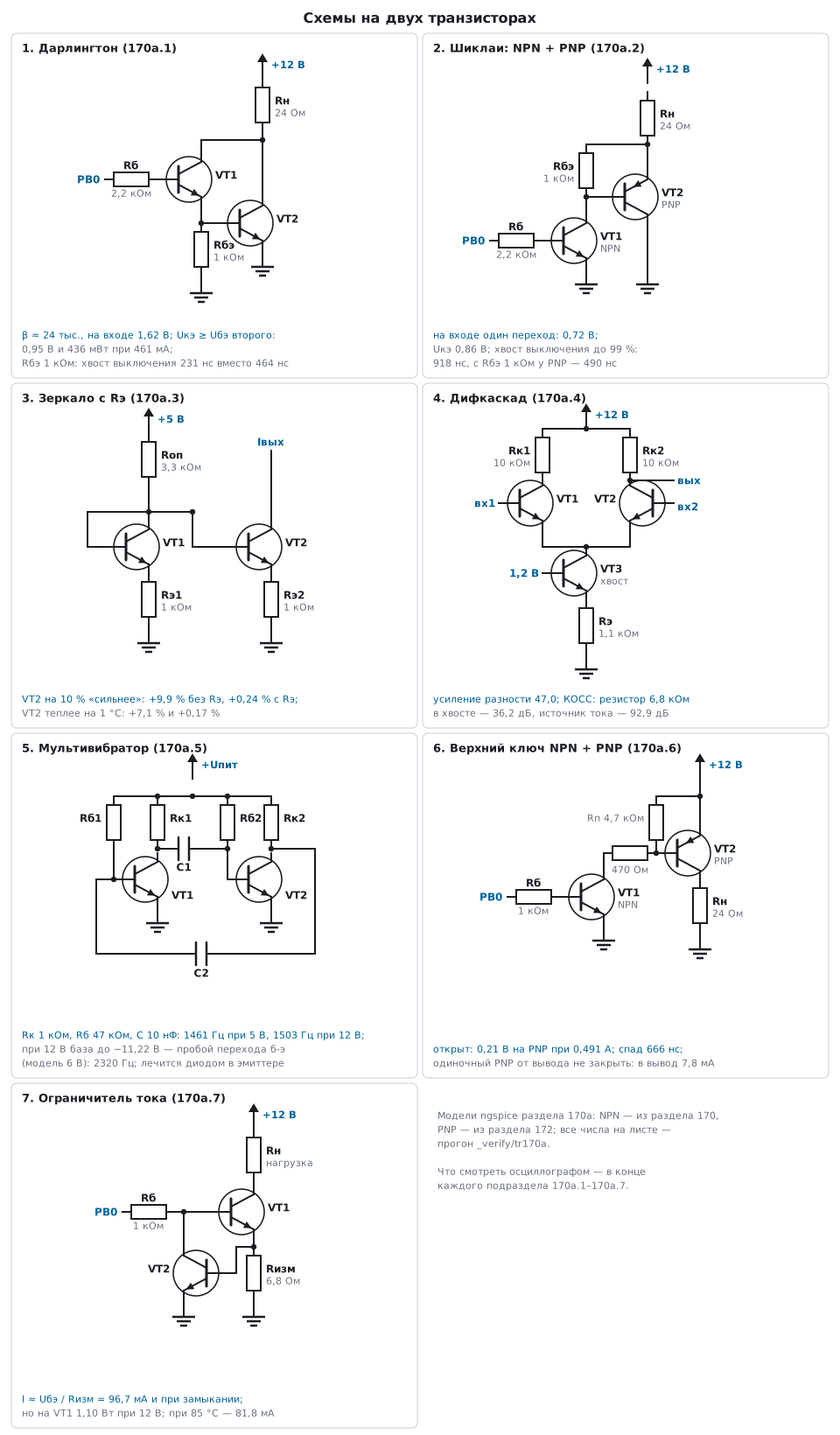
170а.1 Darlington pair
The emitter of the first transistor drives the base of the second, the collectors are common. The base current of the first is amplified twice, and the current gains multiply. In the model, at 10 µA base current and 5 V on the collectors, a single transistor gives a gain of 207, and the Darlington about 24 thousand.
The price is two base-emitter junctions in series. The input of the pair needs not 0.65 V but the sum of two: 1.51 V at 10 µA base current and 1.62 V at a load current of 0.46 A. And it saturates poorly: the first transistor cannot pull the collector below the base of the second, so the VCE of the pair is never less than the VBE of the second.
The switch: a 24 Ω load from 12 V, the base from a 3.3 V pin through 2.2 kΩ.
| Circuit | Base current | VCE | Load current | Heat in the switch |
|---|---|---|---|---|
| single NPN | 1.13 mA | 8.12 V | 162 mA | 1.31 W |
| Darlington | 0.76 mA | 0.95 V | 461 mA | 436 mW |
| Sziklai (170а.2) | 1.17 mA | 0.86 V | 464 mA | 400 mW |
The single transistor does not get enough base current: it stays in the active region, the load gets a third of the current, and the transistor itself dissipates 1.31 W. To saturate it with a forced beta of 20 (section 170.3), you need 23 mA into the base — an MCU pin cannot supply that. The Darlington saturates from 0.76 mA, but 0.95 V remains across it: 0.91 V of that is the VBE of the second transistor. At half an ampere that is almost half a watt.
Slow turn-off and the base-emitter resistor. When the pin goes low, the first transistor turns off, and the charge in the base of the second has nowhere to go: the base-emitter junction of the first is reverse-biased for it. The second transistor stays on, living off its own charge. A resistor between the base and the emitter of the second gives this charge a path to ground. The time from the falling edge on the pin to 50, 90 and 99 % of the collector voltage:
| Variant | 50 % | 90 % | 99 % |
|---|---|---|---|
| no resistor | 159 ns | 256 ns | 464 ns |
| 1 kΩ base-emitter of the second | 155 ns | 208 ns | 231 ns |
| 220 Ω base-emitter of the second | 148 ns | 180 ns | 188 ns |
Up to half the voltage all variants are the same — this is the storage time of the saturated first transistor. The resistor cuts the tail: 99 % in 231 ns instead of 464 ns with 1 kΩ, and in 188 ns with 220 Ω. There is a second benefit: when hot, the leakage current of the first transistor also flows through this resistor instead of being amplified by the second. The price is that the resistor takes part of the current: the VCE of the on switch with 220 Ω is 0.96 V instead of 0.95 V.
On the oscilloscope. Channel 1 is the MCU pin, channel 2 the collector, trigger on the falling edge of channel 1. Without the resistor you see a "shelf" and a long tail before the collector reaches 12 V; with the resistor the tail is shorter. If the collector signal is taken with a 1:10 probe and a long ground lead, the tail is easy to confuse with ringing — use the ground spring from section 36а.2.
Try it in the app: Lab → bench "Two transistors".
170а.2 Sziklai pair: a compound transistor from NPN and PNP
The input is an NPN, the output a PNP. The NPN collector pulls the PNP base down; the PNP emitter is the "collector" of the whole pair, and the PNP collector is tied to the NPN emitter — that is its "emitter". From outside the pair behaves like one NPN with high gain: about 33 thousand in the model at 10 µA base current.
The main difference from the Darlington is one junction at the input: 0.67 V at 10 µA of base current and 0.72 V with the half-ampere load, not 1.51 and 1.62 V. The NPN closes the feedback loop inside the pair: it alone sets the input voltage. That is why Sziklai pairs are used in amplifier output stages — a follower built on one lags the input by one VBE, not two.
Saturation is just as incomplete: the VCE of the pair is at least the VEB of the PNP plus a saturated NPN, 0.86 V in the model (0.84 V of it is the VEB of the PNP). Heat is 400 mW at 464 mA, slightly less than the Darlington.
The Sziklai pair turns off more slowly: without a resistor, the PNP base is floating. From the falling edge on the pin to 50 and 99 % of the voltage:
| Variant | 50 % | 99 % |
|---|---|---|
| no resistor | 355 ns | 918 ns |
| 1 kΩ base-emitter of the PNP | 341 ns | 490 ns |
The rule is the same: a resistor between the base and the emitter of the output transistor.
On the oscilloscope. The same switch as in 170а.1: compare the turn-off tail of the Darlington and the Sziklai pair on one sweep — the Sziklai tail is twice as long while the PNP has no resistor.
Try it in the app: Lab → bench "Two transistors".
170а.3 Current mirror: accuracy and where it breaks
The mirror from 170.6: VT1 is diode-connected, VT2 copies its current. There two errors were shown — the base currents (about 2/β) and the Early effect. In a real circuit two more are added, and they are larger.
Different transistors. The mirror works only if both carry the same current at the same VBE. The reference current is 1.01 mA, the output at 2 V:
| What differs | Output current | Error |
|---|---|---|
| nothing | 1.015 mA | — |
| VT2 has a 10 % larger saturation current (another unit) | 1.116 mA | +9.9 % |
| VT2 is 1 °C warmer | 1.087 mA | +7.1 % |
One degree is already 7 %: at constant VBE the current rises by about 7 % per degree. If VT2 heats up from its own current and VT1 does not, the mirror drifts by tens of percent. That is why a mirror pair is taken in one package — on one die the transistors are identical and share one temperature.
Emitter resistors. 1 kΩ in the emitter of each, the reference current through 3.3 kΩ, about 1.01 V across the resistors. Now the current is set mainly by the drop across the resistor, and a VBE difference of a few millivolts is negligible against a volt:
| What differs | No resistors | With 1 kΩ resistors |
|---|---|---|
| VT2 saturation current 10 % larger | +9.9 % | +0.24 % |
| VT2 is 1 °C warmer | +7.1 % | +0.17 % |
| output at 10 V instead of 2 V (Early effect) | +7.9 % | +0.25 % |
Different resistors give a ratio mirror: 1 kΩ for VT1 and 500 Ω for VT2 — 1.963 mA at the output, 1.94 times the reference.
Leaving the operating range. The mirror holds its current until the output transistor saturates. Simple mirror: 0.998 mA at 0.3 V on the output, 0.996 mA at 0.2 V, 0.959 mA at 0.1 V. With 1 kΩ resistors the lower limit rises by the drop across the resistor: 1.0024 mA at 1.3 V, 1.0020 mA at 1.2 V, 0.989 mA at 1.1 V and already 0.884 mA at 1.0 V. Accuracy is paid for with voltage: less is left for the load.
On the oscilloscope. Feed the mirror load from a generator with a 0…10 V ramp through a 1 kΩ sense resistor; channel 1 is the voltage on the mirror output, channel 2 the voltage across the sense resistor (1 mV is 1 µA), X-Y mode. The screen shows the output characteristic: a sloped horizontal line (Early) and a knee near zero. Breathe on VT2 or touch it with a finger — the horizontal line creeps up.
Try it in the app: Lab → bench "Two transistors".
170а.4 Differential pair
Two transistors with joined emitters share one current — the tail current. Whichever base is higher takes more. The pair amplifies the difference between the base voltages and almost ignores their common level: the input of every op-amp and comparator is built on this.
Model: 12 V supply, 10 kΩ in each collector, both bases biased at 4 V, the output is the collector of VT2. The tail in two ways: a 6.8 kΩ resistor to ground (the "long tail") and a third transistor as a current source (base at 1.2 V, 1.1 kΩ in the emitter).
| Long tail 6.8 kΩ | Tail is a current source | |
|---|---|---|
| tail current | 0.498 mA | 0.515 mA |
| differential gain | 47.0 | 48.4 |
| common-mode gain | 0.726 | 0.00109 |
| CMRR | 36.2 dB | 92.9 dB |
| common level 3 → 5 V: collector shift | 1.45 V | 2.2 mV |
The differential gain is almost the same: it is set by the current,
RC·Itail/(4·φT) — 48.5 at a tail current of 0.498 mA and φT = 25.7 mV.
If you take the output between the collectors it is twice as large, 94.1.
But the resistor lets the common level through: both bases go up — the
emitters go up, the current through the resistor grows, both collectors fall. The common-mode
gain is almost RC/(2·Rtail) = 0.735, and the CMRR is only 36.2 dB.
A current source in the tail holds the current at any level, and the CMRR rises to
92.9 dB. Real input stages are built this way: the tail is always
a current source, usually a mirror.
The linear range is tens of millivolts. The current splits following the hyperbolic tangent: at a 10 mV difference VT1 takes 59 % of the tail, at 57.5 mV 90 %, at 119 mV 99 %, and beyond that the pair is simply switched. Without feedback it is a comparator, not an amplifier; it is made linear by emitter resistors or by external feedback, as in an op-amp (section 56).
On the oscilloscope. Common-mode test: drive both bases through capacitors from one generator output, a 1 kHz sine of 1 V peak-to-peak on top of the 4 V bias. With the long tail the collector shows about 0.73 V peak-to-peak, with the current source about a millivolt, at the level of the probe noise. Channel 1 and channel 2 on the collectors, math A − B is the output between the collectors.
Try it in the app: Lab → bench "Two transistors".
170а.5 Astable multivibrator
Two switches, each holding the other off through a capacitor. When VT1 turns on, its collector drops from the supply almost to zero and through the capacitor drags the base of VT2 below zero. VT2 stays off until its base charges through RB back up to the threshold; then VT2 turns on and turns VT1 off the same way. Section 179.1 builds an oscillator on a comparator — here it is the same thing on two transistors.
Half the period is the time the base takes to rise from −(VCC − VBE)
to the threshold while charging through RB towards +VCC: t ≈ RB·C·ln 2, hence
f ≈ 1/(1.38·RB·C). RC 1 kΩ, RB 47 kΩ, C 10 nF:
| Variant | Frequency | VT1 base, minimum | 2 µs after the edge |
|---|---|---|---|
calculation 1/(2·ln 2·RB·C) |
1535 Hz | — | — |
| 5 V | 1461 Hz | −4.26 V | −4.23 V |
| 12 V | 1503 Hz | −11.22 V | −11.13 V |
| 12 V, base-emitter breakdown at 6 V | 2320 Hz | −10.34 V | −6.05 V |
| 12 V, breakdown at 6 V and a diode in the emitter | 1545 Hz | −9.78 V | −9.70 V |
The formula holds while the supply is much larger than VBE: at 5 V the frequency is 5 % below the calculation.
The base swings down to minus the supply. The base of the off transistor goes to −4.26 V at 5 V and to −11.22 V at 12 V. But the reverse voltage of the base-emitter junction of ordinary small-signal transistors is about 5–6 V (the exact value is the VEBO parameter in the transistor documentation). At 5 V there is still margin, at 12 V there is none: the junction breaks down, the base sticks at −6.05 V, and the frequency goes up to 2320 Hz — 54 % higher. In the model the breakdown is a diode with BV = 6 V across the junction: the transistor model itself has no such parameter. Repeated breakdown also degrades the gain of the transistor over time.
The cure is a signal diode in series with the emitter: it takes the reverse voltage. The frequency returns to 1545 Hz, but the low level of the collector rises from 0.02 to 0.72 V — by the diode drop.
On the oscilloscope. Channel 1 is the VT1 collector, channel 2 the VT1 base, both
DC-coupled. The collector is not a square wave: the fall is sharp, and the
rise is rounded, 10–90 % in 22.4 µs — this is RC charging the capacitor,
2.2·RC·C = 22 µs. The base shows a step down by almost the whole supply and an
exponential back up to 0.7 V. If at 12 V the "bottom" of the base is clipped at −6 V,
the junction is breaking down.
Try it in the app: Lab → bench "Two transistors".
170а.6 A 12 V high-side switch from a 3.3 V pin: NPN + PNP
The 24 Ω load must be switched to +12 V with its minus left on ground — a high-side switch (section 172.1). It is tempting to use one PNP: emitter at 12 V, collector to the load, base through a resistor to the MCU pin. It will not work.
A PNP is off only when its base is almost at the emitter, that is about 12 V. The MCU pin cannot go above 3.3 V: in the "1" state the PNP base at 3.3 V is 8.7 V below the emitter, and the transistor is on. In the model the load gets 0.490 A even with "1" on the pin, and 7.8 mA flows into the pin: the current goes from 12 V through the emitter-base junction into the 3.3 V rail. Switching the pin to the high-impedance state does not help either: the pin protection diode to the supply opens, and the same 7.1 mA flow through it into the 3.3 V rail, while the load still gets 0.490 A. No combination of levels turns the switch off, and the MCU supply is back-fed from 12 V.
The right way: a level shift with a second transistor. An NPN at the bottom (base from the pin through 1 kΩ, current 2.53 mA) pulls the PNP base to ground through 470 Ω; the PNP base is pulled up to its emitter by 4.7 kΩ. The pin sees only an NPN with its emitter on ground, and 3.3 V is enough for it.
| State | Load |
|---|---|
| pin 0 | 0 |
| pin 3.3 V | 11.79 V, 0.491 A; 0.21 V and 101 mW on the PNP |
Turn-on takes 33 ns from the pin edge to half the voltage. Turn-off is slower, the PNP is saturated: to 50 % 666 ns, to 10 % 818 ns; with a 1 kΩ pull-up instead of 4.7 kΩ, 619 and 709 ns. The pull-up is needed not only for speed: without it the PNP base floats, and the NPN leakage is enough to turn the switch partly on.
The same circuit with a P-channel MOSFET is section 172.2; at high currents it is better: no base current and no 0.2 V drop.
On the oscilloscope. Channel 1 is the pin, channel 2 the load. The rising edge is almost immediate, the fall comes with a delay of hundreds of nanoseconds. With 20 kHz PWM (period 50 µs) this is about 1.6 % of the period — irrelevant for a lamp or a motor, for precise PWM take it into account.
Try it in the app: Lab → bench "Two transistors".
170а.7 A two-transistor current limiter
VT1 is a switch or a source, with the sense resistor Rsense in its emitter. VT2
watches this resistor with its base: as soon as the drop across it reaches
VBE, VT2 turns on and steals the base current of VT1. The load current cannot
exceed I ≈ VBE/Rsense. Rsense 6.8 Ω, 12 V supply, the VT1 base from
a 3.3 V pin through 1 kΩ — the pin also enables the limiter.
| Load | With limiter | Without VT2 | Heat in VT1 |
|---|---|---|---|
| 200 Ω | 59.6 mA | 59.6 mA | 5.4 mW |
| 120 Ω | 94.5 mA | 95.4 mA | 13.9 mW |
| 100 Ω | 96.5 mA | 112.6 mA | 169 mW |
| 30 Ω | 96.6 mA | 175.4 mA | 818 mW |
| short circuit | 96.7 mA | 180.5 mA | 1.10 W |
As long as the load itself limits the current, the circuit is an ordinary saturated switch.
Beyond that the current stays at 96.5–96.7 mA: across the sense resistor at short circuit there is
0.658 V — this is the VBE of VT2, and 0.658 V / 6.8 Ω = 96.7 mA.
All the excess voltage is across VT1. At short circuit it dissipates 1.10 W with a 12 V supply and 2.26 W at 24 V. A small transistor in SOT-23 will not survive that — the limiter protects the load, but not itself. A long short circuit is survived only by a transistor on a heatsink; otherwise you need a limiter that shuts off or folds the current back on a short.
The current depends on temperature. The VBE of VT2 falls by about 1.7 mV per degree: at 85 °C there is 0.556 V across the sense resistor, the limit is 81.8 mA, 15.4 % less than at 25 °C. For protection this does not matter; for a precise current you need an op-amp (section 176а) or a dedicated IC.
Capacitive load. A 100 µF capacitor instead of the resistor charges at a constant 96.6 mA and reaches 10 V in 10.42 ms; the current surge at switch-on is 96.2 mA, no more than the limit.
On the oscilloscope. Channel 1 is the voltage across Rsense (the current), channel 2 the capacitor voltage. Instead of an exponential with a current surge you see a flat 0.66 V shelf on the sense resistor and a straight line on the capacitor.
Try it in the app: Lab → bench "Two transistors".
170а.8 Where to use them and what to use instead
| Circuit | Where it fits | What replaces it |
|---|---|---|
| Darlington | relays, lamps, motors up to hundreds of milliamps from a weak pin | Darlington arrays with diodes for inductive loads (such as ULN2003); at high currents an N-channel MOSFET (section 171) |
| Sziklai | output stage of a follower where a single VBE matters | a ready-made power amplifier or an op-amp with a buffer |
| Current mirror | biasing, active load of a stage, LED current source | a dual matched transistor in one package; a precise source on an op-amp |
| Differential pair | to understand how the input of an op-amp and a comparator works | op-amp (section 56), comparator (section 175), instrumentation amplifier (section 176) |
| Multivibrator | a blinker without an MCU, a test oscillator | an MCU timer, a comparator oscillator (179.1) |
| High-side switch NPN + PNP | tens and hundreds of milliamps, 12–24 V | P-channel with an NPN at the bottom (172.2), a ready-made protected high-side switch |
| Current limiter | protecting an LED, a probe, capacitor charging | an electronic fuse, an LED driver, a current-limited switch |
There are also "resistor-equipped transistors" — one package with a transistor, a base resistor and a base-emitter resistor; with them the high-side switch of 170а.6 is built from two packages without loose resistors. Look up the parameters of specific arrays in their documentation: they were not checked here.
170а.9 Pitfalls
The compound switch runs hot although it is "saturated". The VCE of a Darlington does not fall below the VBE of the second transistor: 0.95 V and 436 mW at 461 mA.
The compound switch turns off with a long tail. The charge in the base of the second has nowhere to go; a 1 kΩ base-emitter resistor shortens the tail to 99 % from 464 to 231 ns.
The Darlington turn-on threshold is 1.5 V, not 0.7. There are two junctions at the input: 1.51 V at low current, 1.62 V at half an ampere. A 1.8 V pin barely drives it.
The mirror currents differ by 7–10 %. Transistors from different packages or at different temperatures: 1 °C gives 7.1 %. A dual transistor and emitter resistors: with 1 kΩ, 0.17–0.25 %.
A mirror with resistors "loses" current at a low load voltage. The output needs headroom for the emitter drop: at 1.0 V instead of 1.2 V the current falls from 1.0020 to 0.884 mA.
A differential pair with a resistor in the tail rejects common-mode noise poorly. CMRR 36.2 dB; with a current source in the tail, 92.9 dB.
A 12 V multivibrator runs at the wrong frequency and "ages" over time. The base goes to −11.22 V and breaks down the base-emitter junction; the frequency is 2320 Hz instead of 1503 Hz. Use a diode in the emitter.
The PNP of a high-side switch does not turn off from the pin. The pin cannot raise the base to 12 V; with "1" and in the high-impedance state the load gets 0.490 A, and the 3.3 V rail is back-fed through the pin. Use a second transistor at the bottom.
The current limiter burned out on a short circuit. The whole supply voltage is across VT1: 1.10 W at 12 V, 2.26 W at 24 V.
The limit "drifted" in the heat. 81.8 mA at 85 °C instead of 96.7 mA at 25 °C: the threshold is VBE, and it depends on temperature.
170а.10 Summary
- Darlington: gain about 24 thousand, 1.51–1.62 V at the input, VCE no lower than the VBE of the second — 0.95 V and 436 mW at 461 mA; a base-emitter resistor on the second shortens the turn-off tail from 464 to 231 ns (1 kΩ).
- Sziklai: one junction at the input (0.67–0.72 V), VCE 0.86 V; turn-off without a resistor on the PNP takes 918 ns to 99 %.
- Mirror: a 10 % transistor difference gives +9.9 %, 1 °C gives +7.1 %; 1 kΩ emitter resistors reduce this to 0.24 and 0.17 %, but raise the lower output limit to 1.2 V.
- Differential pair: the differential gain of 47.0 is set by the tail current; CMRR is 36.2 dB with a 6.8 kΩ resistor and 92.9 dB with a current source; it is linear only over tens of millivolts (90 % of the current at 57.5 mV).
- Multivibrator: 1461 Hz at 5 V and 1503 Hz at 12 V against the calculated 1535 Hz; at 12 V the base goes to −11.22 V — a diode in the emitter is needed.
- High-side switch from 3.3 V: a single PNP cannot be turned off; NPN + PNP gives 0.21 V on the switch at 0.491 A, turn-off 666 ns.
- Current limiter: 96.7 mA with 6.8 Ω and at short circuit, but 1.10 W in the transistor and 81.8 mA at 85 °C.
Next: section 171 "Field-effect transistor: regions".