 Embedded HandbookApps
171. Field-effect transistor: principle, regions, threshold and channel resistance, Miller plateau, body diode
Section 52 covered the field-effect transistor as a switch: the gate is a capacitor, a slow edge means heat, high-side and low-side switches. This section is about the device itself: what happens at different gate voltages, why "2 V threshold" does not mean "on at 3.3 V", where the plateau in the gate waveform comes from, how the channel behaves as it heats up, and why a field-effect transistor cannot block current in the reverse direction.
All the numbers below come from ngspice models of two N-channel transistors with explicitly set parameters: a logic-level one (threshold 1.6 V) and a standard one (threshold 3.5 V), otherwise identical.
Terms used in the documentation
Term Meaning gate / drain / source the three terminals of the transistor gate threshold voltage VGS(th) gate-source voltage at which the channel starts to conduct on-state resistance RDS(on) resistance of the fully on channel cutoff / ohmic (linear, triode) / saturation region the three operating regions logic-level MOSFET a transistor specified for logic-level gate drive output characteristics drain current vs drain-source voltage curves total gate charge (Qg) charge needed to bring the gate to the stated voltage gate-drain charge (Qgd), Miller plateau charge of the gate-drain capacitance, the flat step in gate voltage normalized on-resistance vs temperature channel resistance relative to its room-temperature value paralleling connecting transistors in parallel linear mode operation operation with the channel only partly on body diode the parasitic (internal) diode reverse conduction current flowing from source to drain back-to-back MOSFETs two transistors connected in series in opposite directions
171.1 Principle and regions
The gate is separated from the channel by a thin oxide layer — it is a capacitor. When the gate-source voltage is above the threshold, carriers gather at the surface under the gate, and a conducting channel appears between drain and source. The gate draws no DC current; the voltage is what controls the transistor.
| Region | When | How it behaves |
|---|---|---|
| cutoff | VGS below the threshold | off, only leakage flows |
| ohmic region | VGS above the threshold, VDS small | a resistor whose resistance is set by VGS |
| saturation region | VDS greater than VGS minus the threshold | a current source, the value set by VGS |
⚠️ A confusion of words. The "saturation" of a field-effect transistor is the counterpart of the active mode of a bipolar one: the control terminal sets the current. A switch works in the ohmic region — where a bipolar transistor would be in saturation. A switch that has "entered saturation" as a field-effect transistor is not fully on and runs hot.
In a discrete transistor the substrate is tied to the source inside the package, and the drain forms a p-n junction with it. That is the body diode: anode at the source, cathode at the drain (for an N-channel device).
171.2 Output characteristics
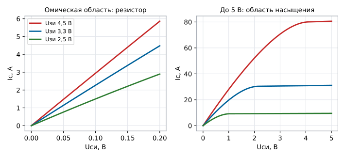
Drain current of the logic-level transistor vs drain-source voltage:
| VGS | Current at VDS 0.1 V | Resistance | Current at VDS 5 V |
|---|---|---|---|
| 2.5 V | 1.50 A | 66.6 mΩ | 9.5 A |
| 3.3 V | 2.27 A | 44.1 mΩ | 31.1 A |
| 4.5 V | 2.94 A | 34.0 mΩ | 80.6 A |
At small VDS the lines start from zero — this is the ohmic region: the transistor is a resistor, and the higher VGS, the smaller it is. At large VDS the current stops growing with the drain voltage and is set by the gate — the saturation region, and it grows faster than linearly: 9.5 → 31.1 → 80.6 A.
171.3 Threshold is not "on"
A 12 Ω load from 12 V (current up to 1 A), gate from 2.5 to 10 V:
| VGS | Logic-level, threshold 1.6 V | Standard, threshold 3.5 V |
|---|---|---|
| 2.5 V | 65.8 mΩ | off |
| 3.3 V | 43.8 mΩ | 2.25 mA instead of 1 A |
| 4.5 V | 33.8 mΩ | 61.0 mΩ |
| 10 V | 24.8 mΩ | 26.2 mΩ |
The threshold voltage in the documentation is the voltage at which a negligible current flows, usually a quarter of a milliamp: at the threshold the transistor is only beginning to turn on. What matters is the channel resistance at your gate voltage. The logic-level transistor driven from a 3.3 V pin gives 43.8 mΩ and 43.4 mW of heat at one amp; the standard one driven from the same pin passes 2.25 mA — the load does not switch on at all. With 10 V on the gate both are almost the same.
The rule of section 52.4 comes from here: choose the transistor by the channel resistance row at 2.5…4.5 V, not by the threshold.
171.4 Gate charge and the Miller plateau
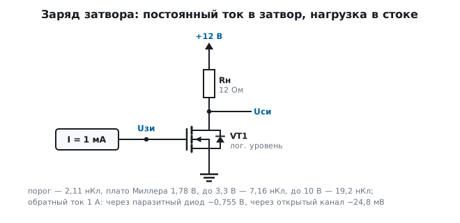
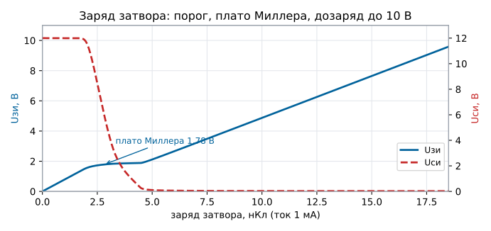
The gate is charged with a constant current of 1 mA; the load is 12 Ω from 12 V. The time in microseconds is numerically equal to the charge in nanocoulombs:
| Point | Charge |
|---|---|
| VGS reached the 1.6 V threshold | 2.11 nC |
| drain fell to 6 V, VGS on the plateau 1.78 V | 2.81 nC |
| VDS below 0.5 V — end of the plateau | 4.34 nC |
| VGS 3.3 V (VDS already 43.6 mV) | 7.16 nC |
| VGS 10 V | 19.2 nC |
While the drain voltage is falling, almost all the gate current goes into recharging the gate-drain capacitance, and the gate voltage stands still — the Miller plateau. From the threshold to the end of the plateau it takes 2.24 nC, and all that time the transistor both conducts current and holds off voltage: it heats up.
What this looks like from an MCU pin: 3.3 V through 470 Ω, on the plateau the gate current is (3.3 − 1.78) / 470 = 3.2 mA, and the plateau lasts 0.69 µs. From a gate driver with hundreds of milliamps — nanoseconds (section 52.3). And a second consequence: the charge to 3.3 V is 7.16 nC, to 10 V 19.2 nC, 2.7 times more; the "total gate charge" in the documentation is given at 10 V.
171.5 Temperature: resistance rises — and that is good
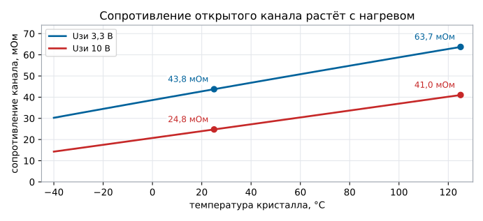
As it heats up, the on-state channel resistance rises: both the channel itself and the bulk of the die below it conduct worse when hot. The same logic-level transistor, a 12 Ω load from 12 V:
| Die temperature | VGS 3.3 V | VGS 10 V |
|---|---|---|
| −40 °C | 30.3 mΩ | 14.3 mΩ |
| 25 °C | 43.8 mΩ | 24.8 mΩ |
| 85 °C | 55.8 mΩ | 34.5 mΩ |
| 125 °C | 63.7 mΩ | 41.0 mΩ |
By 125 °C the resistance at 10 V on the gate has grown 1.66 times, at 3.3 V 1.46 times. The documentation gives the channel resistance at 25 °C, while a hot die is the normal operating state: calculate heat from the resistance at the operating temperature, using the normalized resistance graph in the same documentation.
On the other hand, parallel transistors share current by themselves. Two identical ones on a common 6 Ω load from 12 V (2.00 A), gate at 10 V, one of them 60 °C hotter:
| Transistor | Current |
|---|---|
| VT1, 25 °C | 1.16 A |
| VT2, 85 °C | 0.83 A |
The hot one takes less current and cools down — the current evens out by itself. With diodes and bipolar transistors it is the opposite: the hot one conducts more and pulls the current to itself (169.2).
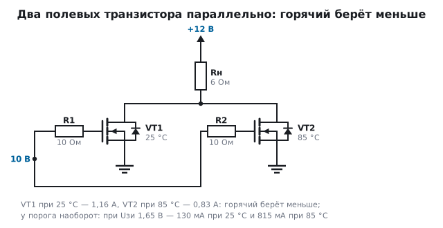
But only when fully on. Near the threshold a different effect dominates: the threshold falls with temperature, and at VGS 1.65 V the current through the same transistor is 130 mA at 25 °C and 815 mA at 85 °C, 6.3 times more. In linear mode — soft start into a capacitance, a current source, an electronic load — the hot transistor turns on harder and pulls the current to itself, like a bipolar one. Field-effect transistors are not paralleled in this mode without balancing resistors in the sources.
171.6 Body diode and reverse current
Let us pass 1 A through the transistor in the reverse direction — from source to drain:
| Gate | VDS |
|---|---|
| 0 V — channel off | −0.755 V |
| 3.3 V | −43.3 mV |
| 10 V | −24.8 mV |
With the channel off the current flows anyway — through the body diode, with its 0.755 V and 0.755 W of heat. With the channel on the same current flows through the channel: the channel conducts in both directions, and the losses are 30.5 times lower.
Three consequences: - a field-effect transistor does not block reverse current — to block both directions (battery protection, switching between two sources), two transistors are placed back-to-back, sources facing each other; - "ideal diode" and reverse polarity protection use the on channel in the reverse direction: 24.8 mV instead of the diode's 0.755 V; - in a bridge, during the dead time, while both switches are off, the load current flows through the body diodes.
171.7 Pitfalls
A transistor with a 2 V threshold does not turn on from 3.3 V. The threshold is a current of a fraction of a milliamp; look at the channel resistance at 2.5 or 4.5 V.
The switch is hot although the transistor is "on". It works in the saturation region, not in the ohmic one: not enough gate voltage.
Heat in the switch is higher than calculated. It was calculated from the channel resistance at 25 °C, and at 125 °C it is 1.66 times higher.
There is a "step" in the gate waveform and the edge is slow. The Miller plateau: recharging of the gate-drain capacitance; from an MCU pin through 470 Ω, 0.69 µs.
The driver was sized by the "total gate charge", and the edge is worse. The edge
is set not by the total charge but by the Miller charge at your drain voltage,
divided by the gate current on the plateau, (Vdrive − Vplateau) / R, — not by the peak
driver current. From a 3.3 V pin through 470 Ω a peak current of 7.0 mA would give
a 0.32 µs plateau, but 3.2 mA flows on the plateau, and it lasts 0.69 µs. If the drain
voltage is higher than in the documentation row, the Miller charge is even larger.
Parallel transistors in a soft-start circuit: one burned out. Near the threshold the hot one turns on harder; in linear mode use source resistors or a single transistor with margin.
A switch that is off passes current at reverse polarity. The body diode; use two back-to-back transistors or an "ideal diode" on a field-effect transistor.
Confusing the "saturation" of a field-effect transistor with bipolar saturation. For a field-effect transistor the switch works in the ohmic region.
171.8 Summary
- Field-effect transistor regions: cutoff, ohmic region (a resistor — the switch), saturation region (a current source — not a switch).
- Logic-level at 1 A: 65.8 / 43.8 / 33.8 / 24.8 mΩ at VGS 2.5 / 3.3 / 4.5 / 10 V; the standard one driven from 3.3 V passes 2.25 mA.
- Gate charge: threshold at 2.11 nC, Miller plateau at 1.78 V up to 4.34 nC, to 3.3 V 7.16 nC, to 10 V 19.2 nC.
- Temperature: at 10 V on the gate, 24.8 mΩ at 25 °C and 41.0 mΩ at 125 °C; fully on parallel transistors share current by themselves (1.16 and 0.83 A), near the threshold it is the opposite.
- Reverse current of 1 A: through the body diode −0.755 V, through the on channel −24.8 mV.
Next: section 172 "Switches".