 Embedded HandbookApps
172. Switches: high-side and low-side, gate driver, half bridge and dead time, soft start, analog switch
Section 52 covered choosing a switch for a load, the gate components and relays; section 171 covered the field-effect transistor itself. This section is about the circuits around it: how to put a switch in the positive wire, why you need a driver, what happens in a half bridge without dead time, how not to burn a switch with a current surge into a capacitive load, and how an analog switch differs from a power switch.
All the numbers below come from ngspice models with explicitly set transistor parameters (a logic-level N-channel, a P-channel, bipolar transistors for level shifting).
Terms used in the documentation
Term Meaning low-side / high-side switch a switch between load and ground / between supply and load level shifter a circuit that translates a control signal to another voltage level gate driver a chip or stage that charges and discharges the gate with a large current totem-pole / push-pull output an output with one transistor to the supply and one to ground half bridge high-side and low-side switches in series dead time a pause when both switches of a bridge are off shoot-through / cross conduction current flowing through both bridge switches at once inrush current the current surge at power-on soft start / slew rate control turning a switch on slowly to limit the surge load switch a switch that powers a load on and off analog switch / transmission gate a switch for signals rather than power on-resistance flatness variation of on-resistance with the input voltage
172.1 Low-side switch and high-side switch
A low-side switch is a transistor between the load and ground: the source is at ground, the gate-source voltage equals the MCU pin voltage, and everything is simple. The downside: the load is always connected to the supply, and its "minus" is what gets switched; that is no good for powering modules, but fine for a motor or a lamp.
A high-side switch is a transistor between the supply and the load: it cuts the power completely. An N-channel transistor will not turn on here — its source rises along with the load, and no gate-source voltage is left. There are two options: a P-channel one, which turns on with a low level relative to the supply, or an N-channel one with a bootstrap (voltage boost).
172.2 High-side P-channel switch with a level shifter
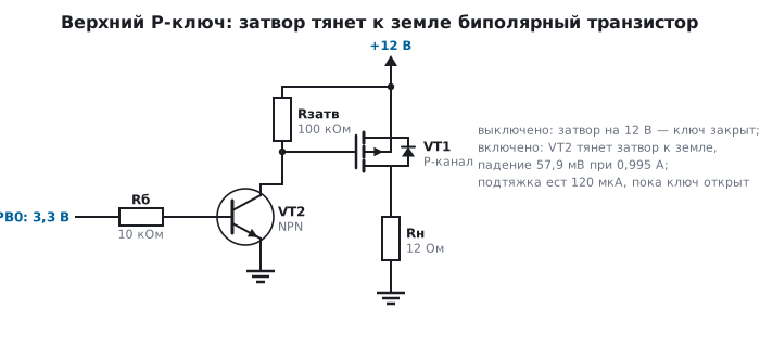
A 12 V supply, a 12 Ω load, control from a 3.3 V pin. The gate of the P-channel transistor is pulled up to 12 V by a 100 kΩ resistor; it is turned on by a bipolar low-side switch that pulls the gate to ground:
| State | Gate | Load |
|---|---|---|
| off, pin at 0 | 12.00 V — same as the source | 0 A |
| on, pin at 3.3 V | 0.01 V | 0.995 A, drop 57.9 mV |
The drop across the on switch is 57.9 mV at 0.995 A, i.e. a channel resistance of 58.2 mΩ. The price of the circuit is a pull-up current of 120 µA while the switch is on: 12 V across 100 kΩ. For a battery-powered device that is a lot, and a larger resistor is used — but then the switch turns off more slowly: it is turned on by the transistor, which pulls the gate to ground quickly, while only the pull-up charges the gate back to the supply. In the model turn-on takes 0.28 µs with any resistor, while turn-off takes 0.52 ms with 100 kΩ and 5.2 ms with 1 MΩ. Slow turn-off means a long pass through the linear region with heating (section 52.3); if that matters, use an active pull-up (a second transistor) or a driver.
⚠️ Look up the gate-source voltage limit in the transistor's documentation. For power transistors it is usually ±20 V, but small ones in SOT-23 can have ±12 V or even ±8 V — then, even in this 12 V circuit, a gate pulled down to 0.01 V is already at the limit or beyond it. If the supply is close to the limit or above it, the gate is not pulled to ground directly: a divider or a Zener diode is placed between gate and source — for a voltage comfortably below the limit.
172.3 Gate driver: why you need one
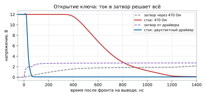
The same N-channel switch on 12 Ω from 12 V, driven in two ways: directly from a 3.3 V pin through 470 Ω and through a push-pull follower made of an NPN and a PNP from 5 V.
| Drive | Half voltage — 6 V on the drain | Fully on — 0.5 V | Energy over 2 µs |
|---|---|---|---|
| 3.3 V pin through 470 Ω | 635 ns | 1141 ns | 1.46 µJ |
| push-pull driver from 5 V | 31 ns | 59 ns | 0.18 µJ |
That is a 19 times difference in time and 8 times in energy. The driver is not "more powerful" — it delivers a large current for the duration of the edge (section 52.2), and on the Miller plateau (section 171.4) it is the current that decides everything. A push-pull follower made of a pair of bipolar transistors is the cheapest current amplifier for a gate. It does not raise the voltage: the output follows the input minus 0.7 V (section 170.5), and in the model a base driven from a 3.3 V pin gives the gate about 2.8 V, although the follower is powered from 5 V. When the gate needs 10 V and the MCU has only 3.3 V, a level shifter is placed before the follower (a transistor with a pull-up, as in 172.2), or a gate driver with an input for 3.3 V logic is used.
172.4 Half bridge: dead time
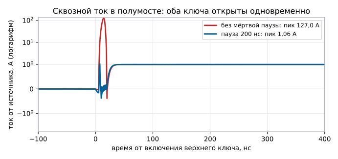
A half bridge is a high-side and a low-side switch in series, with the load at the midpoint. If both turn on at the same time, even for tens of nanoseconds, the supply is shorted to ground through two on channels. The model: 12 V, a 12 Ω load, control edges of 20 ns.
| Dead time | Peak supply current | Average supply current | Average load current |
|---|---|---|---|
| none | 127 A | 1.13 A | 0.61 A |
| 200 ns | 1.06 A | 0.61 A | 0.61 A |
Without dead time the peak shoot-through current is 127 A: that is what a pair of N-channel switches shorted on themselves gives, both on during the overlap of the edges: 12 V / 127 A ≈ 94.5 mΩ for the two. On average 1.13 A is drawn from the supply with a load of 0.61 A: the extra 0.52 A, i.e. 6.3 W, heats the transistors. With a dead time of 200 ns the average supply current equals the load current — there is no shoot-through.
Dead time is set by the MCU timer (section 46.3) or by the half-bridge driver itself. It is also the reason why, during the dead time, the load current flows through the body diodes (section 171.6).
172.5 Soft start into a capacitive load
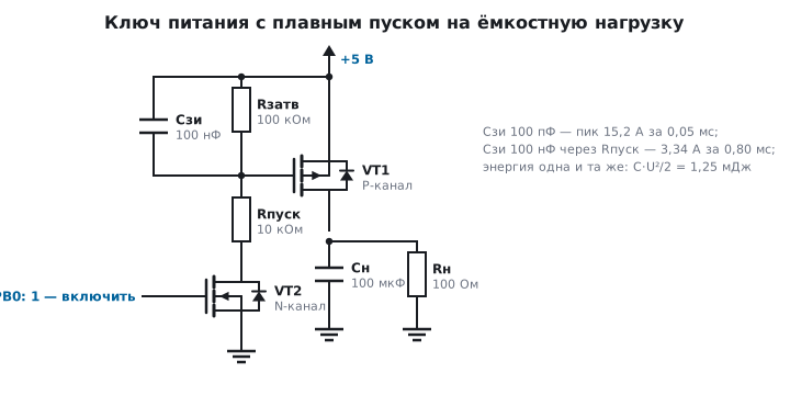
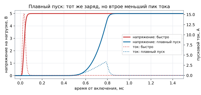
A load switch powers a module that has 100 µF at its input. While the capacitor is empty, it behaves like a short circuit. The same high-side P-channel switch from 5 V; the only difference is the capacitance on the gate:
| Gate | Peak current | Time to reach 4.5 V |
|---|---|---|
| 100 pF — turns on at once | 15.2 A | 0.05 ms |
| 100 nF through 10 kΩ — soft start | 3.34 A | 0.80 ms |
The energy dissipated by the switch is the same — C · V² / 2 = 1.25 mJ
(section 166.3). But in the first case it is released in 0.05 ms — an average
power of 23.6 W, and in the second in 0.80 ms — 1.6 W. Slow turn-on
spreads the heating over time and lowers the current peak, which would otherwise
pull the supply down and reset neighboring modules.
172.6 Analog switch: resistance depends on the signal
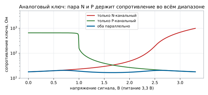
A power switch switches power, an analog switch switches a signal, and it has a different problem: the channel resistance depends on the voltage of the signal, because the gate-source voltage depends on it. A 3.3 V supply, 1 mA flows through the switch:
| Signal voltage | N-channel only | P-channel only | Both in parallel |
|---|---|---|---|
| 0.1 V | 18.3 Ω | 655 Ω | 18.3 Ω |
| 1.65 V | 33.1 Ω | 34.0 Ω | 16.8 Ω |
| 3.2 V | 890 Ω | 18.4 Ω | 18.4 Ω |
A single N-channel switch turns off near the upper rail (890 Ω), a single P-channel one near the lower rail (655 Ω). That is why an analog switch and a multiplexer are internally a pair of N and P in parallel: where one weakens, the other is on. The pair has a resistance of 16.8…20.6 Ω over the whole range, with a maximum of 20.6 Ω at 0.71 V, where the P-channel one is only just beginning to turn on.
What follows on the board: the switch resistance adds to the source resistance and, together with the ADC input capacitance, forms an RC network (section 50.6), and its dependence on the signal is a nonlinearity, i.e. a measurement distortion.
172.7 Pitfalls
An N-channel switch in the positive wire does not turn on. The source has risen along with the load; you need a P-channel one or a bootstrap.
A high-side P-channel switch burned out on a 24 V supply. The gate was pulled to ground: the gate-source voltage exceeds the ±20 V limit — use a divider or a Zener diode.
A small P-channel switch in SOT-23 burned out already at 12 V. Its gate-source limit is ±12 or ±8 V, and the gate was pulled to ground.
A battery device draws an extra few hundred microamps. The gate pull-up of the high-side switch: 12 V across 100 kΩ is 120 µA while the switch is on.
The half-bridge transistors heat up although the load is small. No dead time: a peak shoot-through current of 127 A and an extra 6.3 W on average.
The supply sags when a module is switched on. Inrush current into a capacitive load: 15.2 A instead of 3.34 — you need a soft start.
ADC readings through an analog switch "drift" across the scale. The resistance of a single-transistor switch depends on the signal: 18 Ω near one rail and 890 Ω near the other.
172.8 Summary
- High-side P-channel switch with a level shifter: a drop of 57.9 mV at 0.995 A — 58.2 mΩ, but the gate pull-up draws 120 µA while the switch is on.
- A push-pull driver instead of 470 Ω: fully on in 59 ns instead of 1141 ns, energy over the same window 0.18 versus 1.46 µJ.
- Half bridge without dead time: a peak shoot-through current of 127 A, an extra 0.52 A — 6.3 W; a 200 ns dead time removes it completely.
- Soft start into 100 µF: a peak of 3.34 A instead of 15.2 A; the energy is the same 1.25 mJ, but the average power is 1.6 W instead of 23.6 W.
- Analog switch: single N and P give 890 and 655 Ω near "their" rails, the pair in parallel gives 16.8…20.6 Ω over the whole range.
Next: section 173 "Power and input protection".