 Embedded HandbookApps
170. Bipolar transistor: principle, four modes, saturation, turn-off, current source
Section 51 showed the transistor as a relay switch and how to calculate the base resistor. This section looks inside: how a small base current controls a large collector current, which operating modes exist and how to recognize them by the voltages, why a "switch" can run hot, why it turns off with a delay, how the same transistor makes a current source that does not care what supply it runs from, and what pairs of transistors can do — the mirror and the Darlington.
All the numbers below come from an ngspice model of an NPN transistor with explicitly set parameters (current gain 200, reverse gain 3), roughly a common 0.5 A part.
Terms used in the documentation
Term Meaning base / collector / emitter the three terminals of the transistor DC current gain (hFE) static ratio of collector current to base current cutoff / forward active / saturation / reverse active the four operating modes collector-emitter saturation voltage VCE(sat) collector-emitter voltage of a fully on transistor forced beta the gain you impose by choosing the base current output characteristics collector current vs collector-emitter voltage curves Early effect collector current rising with collector voltage storage time (ts) turn-off delay while stored base charge is removed speed-up capacitor a capacitor across the base resistor Baker clamp (Schottky clamp) a Schottky diode that keeps the transistor out of deep saturation current source / current sink a circuit that sets a current regardless of voltage emitter follower the output on the emitter follows the input current mirror a pair that copies a reference current Darlington pair two transistors where the gains multiply matched pair two transistors with matched parameters
170.1 Principle and four modes
A bipolar transistor is two p-n junctions facing each other: base-emitter and base-collector. The forward-biased base-emitter junction injects carriers into the thin base; almost none of them manage to leave through the base terminal, and they pass on into the collector. That is why the collector current is β times the base current, and it is the base current that controls it, not the collector voltage. More precisely, the collector current is set by the base-emitter voltage: it rises roughly tenfold for every 60 mV of VBE at 25 °C, and the base current is its β-th fraction. For a switch it is more convenient to think in terms of base current, for a mirror (170.6) in terms of voltage.
The mode is determined by which junctions are forward-biased:
| Mode | Base-emitter junction | Base-collector junction | In the model |
|---|---|---|---|
| cutoff | reverse-biased | reverse-biased | collector current 10 pA at 5 V |
| active | forward-biased, 0.73 V | reverse-biased, −4.27 V | IB 100 µA → IC 19.6 mA, β = 196 |
| saturation | forward-biased, 0.73 V | forward-biased, +0.68 V | VCE 0.045 V, IC 9.9 mA at IB 1 mA |
| reverse active | reverse-biased, −4.38 V | forward-biased, 0.62 V | IB 100 µA → 0.30 mA, gain 3.0 |
How to read this on a real board: a multimeter between base and emitter shows about 0.7 V — the junction is forward-biased; if the collector is then almost at the emitter, it is saturation; if it sits volts above, it is the active mode.
Reverse active mode means collector and emitter are swapped: the transistor works, but with a gain of about 3 instead of 200. The switch "sort of turns on", but not fully, and runs hot — a common mistake with the package pinout.
170.2 Output characteristics
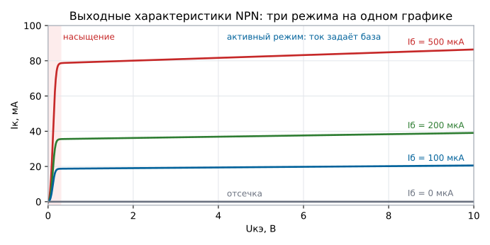
Collector current vs collector-emitter voltage at constant base current:
| Base current | VCE 0.2 V | VCE 5 V | β at 5 V |
|---|---|---|---|
| 100 µA | 18.1 mA | 19.6 mA | 196 |
| 200 µA | — | 37.3 mA | 186 |
| 500 µA | 73.9 mA | 82.5 mA | 165 |
In the active mode the curves are almost horizontal: the base sets the current. Almost — at 10 V the current is 4.8 % higher than at 5 V (the Early effect). The current gain is not constant and falls as the current rises: 196, 186, 165. To the left of 0.2…0.3 V the curves drop down — that is saturation: the base current is "more than enough", and the collector current is now set by the load.
170.3 Saturation: how much current into the base
The switch: a 120 Ω load from 12 V, current up to 100 mA. We vary the base current:
| Base current | Forced β | VCE | IC | Heat in the transistor |
|---|---|---|---|---|
| 0.5 mA | 161 — not saturated | 2.36 V | 80.4 mA | 189 mW |
| 1 mA | 99 | 0.16 V | 98.7 mA | 15.9 mW |
| 2 mA | 49 | 0.13 V | 98.9 mA | 12.5 mW |
| 5 mA | 20 | 0.10 V | 99.2 mA | 9.9 mW |
| 10 mA | 10 | 0.084 V | 99.3 mA | 8.4 mW |
At 0.5 mA the transistor is in the active mode: the load gets less current than it should, and the transistor has 2.36 V and 189 mW across it — 12 times more than at 1 mA. Hence the rule of section 51.5: choose the base current for a forced gain of 10…20, not for the datasheet β, which also falls with current and temperature. Beyond 20 the gain is small: from 5 to 10 mA VCE drops only from 0.10 to 0.084 V.
170.4 Turn-off: storage time
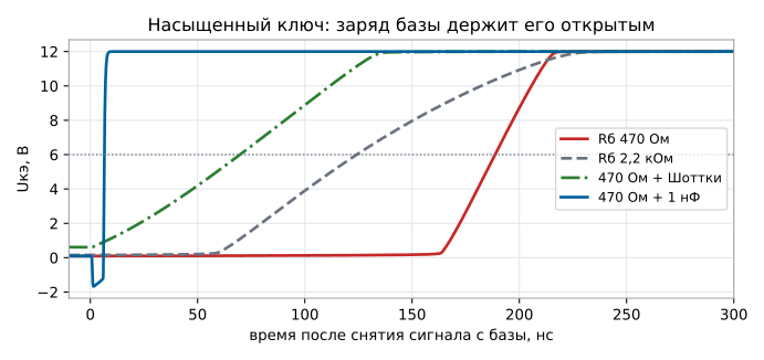
In saturation the base is flooded with charge. When the MCU pin removes the signal, that charge keeps the transistor on for a while longer. The same switch, base driven from a 3.3 V pin:
| Variant | VCE when on | Turn-off delay |
|---|---|---|
| RB 470 Ω (IB 5.5 mA, β 18) | 0.10 V | 189 ns |
| RB 2.2 kΩ (IB 1.2 mA, β 85) | 0.15 V | 124 ns |
| 470 Ω and a 1 nF speed-up capacitor | 0.10 V | 6.5 ns |
| 470 Ω and a Schottky diode base→collector | 0.62 V | 70 ns |
The deeper the saturation, the longer the turn-off — that is the flip side of a large base current. For relays and lamps it does not matter at all; for PWM at tens of kilohertz it hardly matters. But for a software serial port at 1 Mbit/s (bit time 1 µs), 189 ns is 19 % of a bit.
Two techniques: - a speed-up capacitor in parallel with the base resistor — on the edge it pulls the charge out of the base with a current the resistor would not allow; the fastest option, but it loads the pin on the edges; - a Schottky diode between base and collector keeps the transistor out of deep saturation — VCE of the on switch rises to 0.62 V, and it runs hotter.
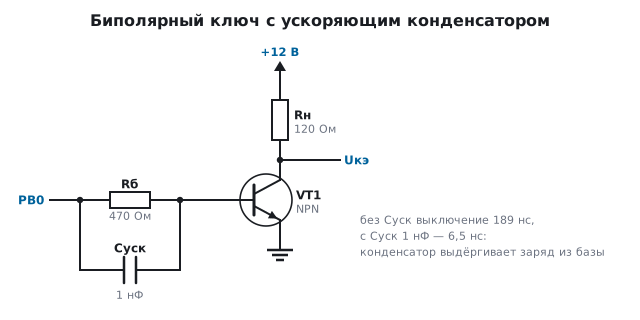
The plot also shows the price of the speed-up capacitor: for a few nanoseconds the collector goes below zero, down to −1.67 V. The base is jerked negative, while the saturated base-collector junction is still forward-biased and drags the collector along with it. This does not harm the load, but if the collector signal goes to an MCU input, this negative swing will flow into the pin's protection diode (section 62).
170.5 The active mode at work: a current source
An LED needs 20 mA, and the supply is sometimes 5 V, sometimes 12 V. Let us compare a resistor with a switch against a transistor in the active mode: base driven straight from a 3.3 V pin through 1 kΩ, 120 Ω in the emitter, the LED in the collector.
| Circuit | 5 V supply | 12 V supply |
|---|---|---|
| 150 Ω resistor and a switch | 19.6 mA | 64.4 mA |
| current source, 120 Ω in the emitter | 20.5 mA | 20.6 mA |
With the resistor the current grew 3.3 times — the LED is overloaded. The current source
changed by 0.4 %: the emitter follows the base minus 0.7 V, so the 120 Ω
always has about 2.5 V across it, and the collector current is almost equal to the emitter current.
IC ≈ (3.3 − VBE) / RE.
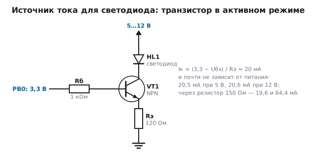
The price is heat and voltage headroom. Everything the supply gives beyond the LED and the emitter resistor drops across the transistor: at 12 V it has 7.54 V and 155 mW. And at the low end the supply must cover the LED (1.99 V), the emitter resistor (2.46 V) and at least 0.2 V across the transistor — about 4.65 V; at 5 V the transistor is left with 0.55 V.
The emitter follower is the same circuit with no load in the collector: the output on the emitter follows the input minus 0.7 V, and it draws β times less current from the signal source than it delivers to the load. This is how a weak output is buffered when no operational amplifier (section 56) is at hand.
170.6 Transistor pairs: current mirror and Darlington
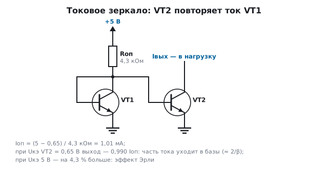
Current mirror. Two identical transistors with common bases and emitters. VT1 is diode-connected — collector tied to base — and the reference current itself sets the required VBE on it. VT2 gets the same VBE and, being identical, passes the same current. The reference current is set by a resistor: (5 − 0.65) / 4.3 kΩ = 1.01 mA.
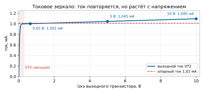
| VCE of the output transistor | Output current | Relative to the reference |
|---|---|---|
| 0.65 V (same as VT1) | 1.001 mA | −1.0 % |
| 2 V | 1.015 mA | +0.3 % |
| 5 V | 1.045 mA | +3.3 % |
| 10 V | 1.095 mA | +8.2 % |
With equal VCE the mirror is 1.0 % low: the two base currents are taken from the reference, which is about 2/β. Beyond that the output current grows with voltage: from 0.65 to 5 V by 4.3 %, to 10 V by 9.3 %. This is the Early effect from 170.2, and because of it a simple mirror is an imperfect current source. Resistors in the emitters of both transistors raise the output resistance and smooth out the VBE spread; and the transistors themselves are truly identical only on one die — which is why a dual transistor in one package is used.
Darlington pair — the emitter of the first drives the base of the second: the current gains multiply. A 120 Ω load from 12 V, base driven from a 3.3 V pin through 10 kΩ:
| Circuit | VCE | IC | Heat in the transistor |
|---|---|---|---|
| single transistor | 6.38 V | 46.8 mA | 299 mW |
| Darlington | 0.80 V | 93.3 mA | 75 mW |
For the single transistor 0.26 mA of base current is not enough — it is stuck in the active mode (6.38 V and 299 mW). The Darlington is fine with 186 µA from the pin, but it does not saturate down to a tenth of a volt: the first transistor cannot pull the collector below the base of the second, so VCE never falls below the VBE of the second — 0.80 V. That is 75 mW, 7.6 times more than a single saturated switch with a 5 mA base current (170.3). With loads of hundreds of milliamps and more, the Darlington switch loses to a field-effect transistor — the subject of the next section.
170.7 Pitfalls
The switch runs hot and the load works "at half power". Base current chosen by the datasheet β — the transistor is in the active mode: 2.36 V and 189 mW instead of 0.16 V.
The transistor turns on, but poorly, although the base current has margin. Collector and emitter are swapped — reverse active mode with a gain of about 3.
Pulses at the switch output are stretched by hundreds of nanoseconds. The storage time of a saturated transistor; use a speed-up capacitor or a Schottky clamp.
A switch with a Schottky clamp runs hotter. VCE when on is 0.62 V instead of 0.10 V: that is how the clamp works.
The current source is hot at a high supply voltage. All the excess voltage drops across the transistor: at 12 V, 155 mW.
The LED current from the current source dropped at 5 V. Not enough headroom: the transistor went into saturation; below 4.65 V the current source stops being one.
The Darlington switch runs hot, although it is saturated. VCE of a Darlington does not go below the VBE of the second transistor: 0.80 V and 75 mW at 93 mA.
The mirror currents differ by percents. Different VCE on the input and output transistors (the Early effect) or transistors from different packages; use a dual transistor and emitter resistors.
170.8 Summary
- The mode is set by the junctions: active — only base-emitter is forward-biased (β = 196), saturation — both are (VCE 0.045 V), reverse active — the terminals are swapped (gain 3.0), cutoff — 10 pA.
- In the active mode the base sets the current; the Early effect adds 4.8 % over 5 V, β falls with current: 196, 186, 165.
- A 100 mA load: IB 0.5 mA — 2.36 V and 189 mW; 1 mA — 0.16 V; 5 mA — 0.10 V.
- Turn-off of a saturated switch — 189 ns; a 1 nF speed-up capacitor — 6.5 ns; a Schottky clamp — 70 ns with VCE 0.62 V.
- Current source: 20.5 mA at 5 V and 20.6 mA at 12 V versus 19.6 and 64.4 mA with a resistor.
- Current mirror: 1.001 mA with a 1.01 mA reference (−1.0 %, base currents), with 10 V at the output +8.2 % (Early effect); a Darlington switch driven through 10 kΩ saturates, but VCE is 0.80 V and 75 mW.
Next: section 170а "Two-transistor circuits: compound pairs, mirror, differential pair, multivibrator, high-side switch and current limiter".