 Embedded HandbookApps
18. The SPI bus
After I²C it feels like a rest: it is simpler, works an order of magnitude faster and needs no pull-ups. The price is more wires and a separate select line for each device. This section takes apart the clock modes at the level of edges — with a model that shows what a byte turns into with the wrong mode — the speeds of the F103 and F407, and three devices that are found in almost every instrument: flash memory, an SD card and a chain of shift registers.
Terms used in the documentation
Term Meaning master / slave the device that drives the clock / the device that answers clock polarity ( CPOL)the idle level of the clock clock phase ( CPHA)which edge the data is read on slave select ( NSS/CS)the line that selects a device full duplex / half duplex exchange in both directions at once / in turn baud rate prescaler the divider that sets the speed busy flag ( BSY)an exchange is still in progress data frame format ( DFF)the width of a transfer MSB / LSB first most / least significant bit first setup / hold time how long data must be stable before / after the edge JEDEC ID the manufacturer and chip identifier daisy chain the output of one device goes to the input of the next latch ( RCLK)transferring the shift register to the outputs overrun ( OVR)a byte received on top of an unread one
18.1 Four wires
| Line | Purpose |
|---|---|
| SCK | the clock, generated by the master |
| MOSI | data from the master to the slave |
| MISO | data from the slave to the master |
| CS (NSS) | device select, active low |
The first three are shared by all devices on the bus, while the select line is separate
for each. Three chips need six pins: three shared plus three
separate CS.
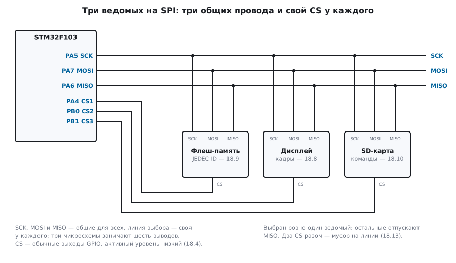
The main property to grasp at once: the exchange is always two-way.
Inside there is a circular shift register — with each clock a bit leaves
the master and at the same time a bit arrives from the slave. In the ordinary
bidirectional mode there is no separate "receive only" operation. (The
RXONLY mode exists, but in it the master drives the clock non-stop while the block is enabled,
and switching it off exactly after the required byte is a separate task.)
Hence an idiom that puzzles at first:
uint8_t spi1_read(void)
{
    return spi1_xfer(0xFFu);
}
The master generates the clock, so for the slave to output something you have to
send something. The value does not matter — usually 0xFF or zeros are sent.
On the F103 and F407 the SPI block is the same: the same CR1 bits, the same SR
flags. The pins and the clocking differ: on the F407 the alternate function
is selected by a number in AFR — for SPI1 it is 5.
18.2 Four modes: CPOL and CPHA
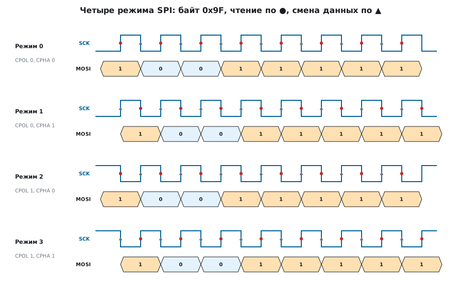
Two bits determine what the clock looks like and when the data is latched:
| Mode | CPOL |
CPHA |
Idle clock | Data is read |
|---|---|---|---|---|
| 0 | 0 | 0 | low | on the rising edge |
| 1 | 0 | 1 | low | on the falling edge |
| 2 | 1 | 0 | high | on the falling edge |
| 3 | 1 | 1 | high | on the rising edge |
CPHA = 0: the first bit is set up even before the first edge, read on
the first edge, changed on the second. CPHA = 1: a bit is set up on the
first edge and read on the second. The common ones are 0 and 3: in both the data
is read on the rising edge, so many chips understand
either of them. Modes 1 and 2 are rare.
What happens with the wrong mode — a model. The master transmits a byte in its own mode, the slave reads in its own; on the edge where the master changes the data, the slave still manages to read the old value — that is how real chips behave, it is the hold time. The result for the byte 0x9F: with the master in mode 1, a slave in mode 0 or 3 reads 0x4F instead of 0x9F — every bit is one clock late, and the first bit read is a zero from the line. A master in mode 0, on the other hand, is read correctly by all four slaves: whether they read on "their" edge or on the change edge, the data at that moment is still the old one.
⚠️ The wrong mode gives no error and may not show up at once. The exchange goes on, bytes arrive — just the wrong ones, or the right ones but only in one direction and only at a low speed. The typical appearance is a shift by one bit or stable garbage that looks like data. If a chip does not answer with the identifier it is obliged to return, check the mode first.
18.3 Speed
It is set by a prescaler from 2 to 256, so nothing is faster than half the bus frequency. There is a second upper limit too — from the chip description: on the F103 the SPI clock is no higher than 18 MHz for both master and slave.
| Bus | Maximum | |
|---|---|---|
SPI1 (F1) |
APB2, 72 MHz | 18 MHz — the limit from the description; a divider of 2 would give 36 MHz |
SPI2 (F1) |
APB1, 36 MHz | 18 MHz |
SPI1 (F4) |
APB2, 84 MHz | 42 MHz |
SPI2, SPI3 (F4) |
APB1, 42 MHz | 21 MHz |
As with the UART, the ports sit on different buses, and one and the same divider gives
different speeds. On the F407 the SPI pins at high speed also need a fast
edge: the OSPEEDR field — otherwise at 21–42 MHz the edges degrade.
Practical guidelines:
- a breadboard build on wires — no higher than 8–10 MHz, otherwise interference;
- a display on a short board — 20–40 MHz, so that frames keep up;
- SD card initialisation — no faster than 400 kHz, then switch to the working speed (section 41). The largest divider of 256 gives 281 kHz on SPI1 of the F1 (328 kHz on SPI1 of the F4) — just within the limit.
18.4 Device select: hardware or manual
The CS line can be controlled in two ways, and the second is almost always chosen.
Hardware — the controller toggles the NSS pin itself. On the F1 and F4 it goes low
when the master starts an exchange, and goes high only when the block is disabled
(SPE = 0). So it suits a single slave, and the end of a transaction
has to be marked by disabling SPI. The new-style blocks also have a pulse
between transfers (NSSP, 18.12) — it deselects the device between bytes
and breaks multi-byte commands.
Software — you declare CS an ordinary output and control it yourself.
This is almost always done: it is predictable and lets you keep the select active
for the whole transaction.
SPI1->CR1 = SPI_CR1_MSTR | SPI_CR1_SSM | SPI_CR1_SSI | (br << 3); /* режим 0, 8 бит */
Both bits are mandatory: SSM switches control to software mode,
and SSI sets the internal level. Forget SSI — and the controller will decide that it
has itself been selected by another master, and will leave master mode.
18.5 🔧 Exchanging a block of data
void spi1_transfer_block(const uint8_t *tx, uint8_t *rx, uint32_t len)
{
    CS_LOW();
    for (uint32_t i = 0; i < len; i++) {
        uint8_t in = spi1_xfer(tx ? tx[i] : 0xFFu);
        if (rx) {
            rx[i] = in;
        }
    }
    /* RXNE говорит лишь о принятом байте; последний бит может ещё уходить. */
    while (SPI1->SR & SPI_SR_BSY) { }
    CS_HIGH();
}
⚠️ Before releasing
CS, wait forBSYto clear. TheRXNEflag means that the received byte is in the register, but the last bits may still be on the line. Release the select earlier — and you cut off the tail of the transfer. It shows up as "sometimes works": at a low speed it manages, at a high one it does not.
18.6 SPI and DMA
For streaming tasks — output to a display, reading flash memory, receiving from an ADC — byte-by-byte exchange in a loop eats the whole processor. A 240×320 display frame in 16 bits is 150 kilobytes that must be pushed through as fast as possible.
DMA is mandatory here (section 9). For two-way exchange two
streams are needed — one for transmission, the other for reception. If reception is not needed (output
to a display), one transmit stream is enough: the receive overrun flag
OVR will be set, but it does not stop transmission — only the
received bytes are lost. So after the transmission read DR and SR once each —
this clears RXNE and OVR, otherwise the next reception will return an old byte.
18.7 What else the block can do
16-bit transfers. The DFF bit switches the width. For displays
where a colour is encoded in 16 bits, this halves the number of operations
and the load on the bus. DFF can be changed only with the block disabled:
SPI1->CR1 &= ~SPI_CR1_SPE;
SPI1->CR1 |= SPI_CR1_DFF;
SPI1->CR1 |= SPI_CR1_SPE;
Half duplex. One data line instead of two, the direction is switched in software. It saves a pin and is used in some sensors and displays.
Slave mode. The microcontroller can itself be a slave — for example, a subordinate module in a large system. Then the clock is generated by an external master, and you must keep up with it, which almost always means DMA. How much time there is for this and how the protocol is built — section 17а.
Hardware CRC calculation. The block can compute the checksum of the transmitted data itself — useful in a noisy environment.
I²S on the F407. SPI2 and SPI3 support the I²S audio interface — the same
block in another mode: digital audio for codecs and microphones.
18.8 A display: frame time
A frame of 240 × 320 pixels at 16 bits is 1 228 800 bits. The limit set by the SPI speed:
- F103,
SPI1at 18 MHz (the limit from the description, divider 4): 68.27 ms, no more than 14.6 frames per second; - F407,
SPI1at 42 MHz (divider 2): 29.26 ms, no more than 34.2 frames per second.
This is the time without a single pause between words. A loop polling TXE at such a
speed leaves pauses — the processor cannot put a word in the same
clock cycle in which the register became free — and the real frame rate is lower.
So for a display — 16-bit transfers and DMA, while the processor meanwhile
prepares the next piece of the frame. If it must be faster — redraw
only the changed areas: display controllers have window commands
for this.
Filling with a colour in 16-bit mode, without reception:
while (!(SPI1->SR & SPI_SR_TXE)) { }
SPI1->DR = color;
18.9 🔧 The JEDEC flash memory identifier
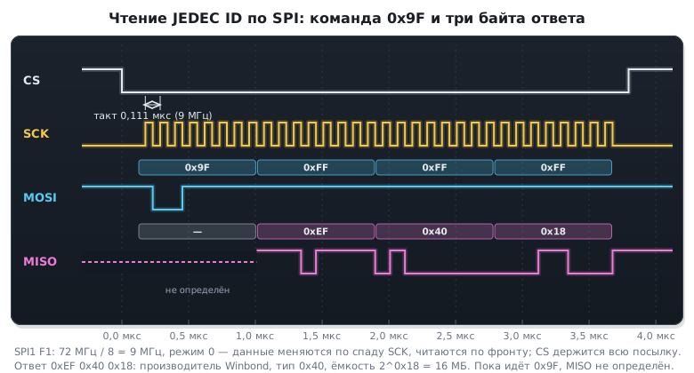
The first thing done with a new SPI flash: read the identifier. The command 0x9F, and three bytes in reply — the manufacturer (0xEF for Winbond), the memory type and the capacity as a power of two. If 0xFF arrived — there is no answer (MISO hangs at one), if 0x00 — the pin is pulled to ground or the chip is not selected. The function is the same for the F103 and F407:
void flash_jedec_id(uint8_t id[3])
{
    CS_LOW();
    spi1_xfer(0x9F);
    id[0] = spi1_xfer(0xFF);     /* производитель: 0xEF — Winbond */
    id[1] = spi1_xfer(0xFF);     /* тип памяти */
    id[2] = spi1_xfer(0xFF);     /* ёмкость: 2^id[2] байт */
    spi1_done();
    CS_HIGH();
}
The reply to the first byte — 0x9F — is skipped: while the command is going out, the chip does not know anything yet and returns garbage. A correct identifier is the best check of the mode, the speed and the wiring at once: writing and erasing (section 41) are tried only after it.
This is what reading the identifier looks like on the analyzer screen:
18.10 An SD card: the command frame and CRC7
In SPI mode an SD card accepts commands in 6-byte frames: 01 and the command number, 32 bits of argument, CRC7 and a stop one. After switching to SPI mode (CMD0 with CS low) CRC checking is disabled — except for CMD8: the card always checks it. So a correct CRC is needed for two commands, CMD0 and CMD8. It is computed like this:
uint8_t sd_crc7(const uint8_t *p, int n)
{
    uint8_t crc = 0;
    int i, b;
    for (i = 0; i < n; i++)
        for (b = 7; b >= 0; b--) {
            int in = ((p[i] >> b) & 1) ^ ((crc >> 6) & 1);
            crc = (uint8_t)((crc << 1) & 0x7F);
            if (in)
                crc ^= 0x09;
        }
    return (uint8_t)((crc << 1) | 1);
}
The check is two frames known to everyone who has brought an SD card to life: CMD0 — 0x40 00 00 00 00 95, CMD8 with the argument 0x1AA — 0x48 00 00 01 AA 87. Before CMD0 the card must receive at least 74 clocks with the select released — that is ten transfers of 0xFF, and all of this at a speed of up to 400 kHz (18.3); the full card start-up order is in section 41.
18.11 🔧 A chain of 74HC595 shift registers
When there are not enough pins, outputs are added with 74HC595 shift registers:
each has 8 outputs, the output of the last bit is connected to the input
of the next, and three chips give 24 outputs on three wires — the clock,
the data and the RCLK latch. There is no reception, MISO is not needed. The chip itself and its inputs are in section 22.1.
The byte order is the opposite of the intuitive one: the first byte sent is pushed furthest. A model of the chain: C3, 5A, 81 were sent — the register nearest to the microcontroller holds 81, the furthest C3. So the byte for the furthest register goes out first:
void hc595_write3(const uint8_t v[3])
{
    spi1_xfer(v[2]);
    spi1_xfer(v[1]);
    spi1_xfer(v[0]);
    spi1_done();                 /* последний бит должен дойти до регистра */
    RCLK_HIGH();                 /* фронт защёлки — все 24 выхода меняются разом */
    RCLK_LOW();
}
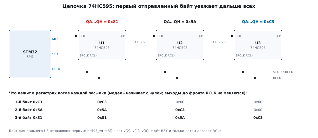
The latch is the main convenience: while the bytes travel along the chain, the outputs stay
as they were, and all 24 change on one edge. Toggling it before BSY clears
means latching a value that has not been fully shifted in.
18.12 F0 and G0: the width in DS and a byte in DR
The SPI registers of the F0 and G0 are where they are on the F1: CR1 0x00, CR2 0x04,
SR 0x08, DR 0x0C. The CPOL/CPHA modes, the BR divider, software
NSS via SSM/SSI — all the same. There are two differences, and both concern the width.
There is no DFF bit. The transfer width is set by the four-bit DS field
in CR2: any value from 4 to 16 bits, the number minus one — 0111 for
8 bits, 1111 for 16. Code with SPI_CR1_DFF does not build on the F0:
use of undeclared identifier 'SPI_CR1_DFF'.
    SPI1->CR2 = (7u << SPI_CR2_DS_Pos) | SPI_CR2_FRXTH;  /* 8 бит; RXNE — как только есть байт */
    SPI1->CR1 = SPI_CR1_MSTR | SPI_CR1_SSM | SPI_CR1_SSI | SPI_CR1_BR_1;   /* /8 */
    SPI1->CR1 |= SPI_CR1_SPE;
DR has a FIFO. Behind the data register there are FIFOs of four bytes
in each direction; their fill level is seen in SR — the FTLVL and FRLVL fields.
Hence the rule: with transfers of up to 8 bits DR is accessed as a byte.
The ordinary write SPI1->DR = b is 16-bit, and the block puts two bytes into the FIFO:
b and a zero go out on the line, and reception gets out of step by one byte. The FRXTH bit
makes RXNE rise already at one received byte, not at two:
uint8_t spi1_xfer_f0(uint8_t out)
{
    *(volatile uint8_t *)&SPI1->DR = out;       /* именно байт: 16-битная запись кладёт в очередь два */
    while (!(SPI1->SR & SPI_SR_RXNE)) {
    }
    return *(volatile uint8_t *)&SPI1->DR;
}
This is visible in the object file: the exchange compiles into STRB and LDRB, not
into STRH/LDRH. The block exchange from 18.5 and all the recipes below carry over
to the F0/G0 by replacing this one function.
The rest — by the table:
| F1 | F0 | G0 | |
|---|---|---|---|
| SPI1 clock | APB2ENR |
APB2ENR |
APBENR2 |
SCK/MISO/MOSI on PA5/PA6/PA7 |
default AF | AF0 | AF0 |
PCLK for SPI1 at maximum |
72 MHz | 48 MHz | 64 MHz |
SCK with a divider of 8 |
9 MHz | 6 MHz | 8 MHz |
The new block also has an NSS pulse between transfers (NSSP in CR2)
and a hardware CRC of any length (CRCL); neither is needed for the displays
and flash memory of this section.
18.13 Pitfalls
The chip does not answer. Check in order: the mode (CPOL/CPHA),
whether MOSI and MISO are swapped, whether CS reached the right pin,
whether there is power and a common ground. The JEDEC identifier (18.9) is a quick test.
SSI is not set. The controller leaves master mode.
Data gets cut off at high speed. CS is released before BSY clears.
A shift by one bit. Almost always the wrong clock phase: in the model 0x9F turns into 0x4F.
Garbage with several devices. Two CS are active at the same time, or
inactive devices do not release MISO. Decent chips put
MISO into a high-impedance state when deselected, cheap ones do not always.
An SD card releases MISO only after a clock with CS high: after each
transaction with it one empty byte 0xFF is sent with CS already high.
Interference on long wires. SPI has neither pull-ups nor error checking: a corrupted bit simply becomes a different byte. On a breadboard lower the speed.
The display works, the flash does not (or the other way round) on the same bus. The devices need different modes or different speeds — reconfigure the controller before accessing each one.
After output to the display, reception is broken. It transmitted without reading, and
OVR was set. Read DR and SR.
The SD card does not answer CMD0. A wrong CRC, too few clocks before the command or a speed above 400 kHz.
The bytes on the 74HC595 outputs are mixed up. They were sent in direct order — the byte for the furthest register must go out first.
18.14 Summary
- The exchange is always two-way: to receive a byte, you have to transmit one.
- The mode is set by
CPOLandCPHA; the common ones are 0 and 3. The wrong mode gives no error: in the model 0x9F reads as 0x4F, and sometimes correctly — for a while. - The speed is no higher than half the bus frequency and the limit from the chip description:
SPI1— 18 MHz on the F103 and 42 MHz on the F407. - Control the device select in software, setting both the
SSMandSSIbits. - Before releasing
CSand before the latch wait forBSYto clear. - A 240 × 320 × 16-bit display frame takes 68.27 ms on the F103 and 29.26 ms on the F407 without pauses; beyond that, only DMA and partial redrawing.
- The JEDEC identifier is the first check of a flash memory; an SD command frame with CRC7: CMD0 ends in 95.
- Each device has its own select line; only
SCK,MOSI,MISOare shared.
Full sources
spi18.c — SPI1 as master on the F103 and F407: the flash memory identifier, the 74HC595, an SD card command, transfers to a display.
/* Раздел 18 (обогащение): SPI1 ведущим на F103 и F407 — идентификатор флеш-памяти,
 * цепочка 74HC595, кадр команды SD-карты, 16-битные посылки для дисплея.
 * Собирается armclang с -include stm32f10x.h (STM32F10X_MD) или stm32f4xx.h (STM32F407xx). */
#include <stdint.h>

#if defined(STM32F10X_MD)
#define PCLK2_HZ 72000000u               /* SPI1 на APB2 */
#define PCLK1_HZ 36000000u               /* SPI2 на APB1 */
#else
#define PCLK2_HZ 84000000u
#define PCLK1_HZ 42000000u
#endif

#define CS_LOW()    (GPIOA->BSRR = 1u << (4 + 16))
#define CS_HIGH()   (GPIOA->BSRR = 1u << 4)
#define RCLK_LOW()  (GPIOA->BSRR = 1u << (3 + 16))
#define RCLK_HIGH() (GPIOA->BSRR = 1u << 3)

/* PA5 SCK, PA6 MISO, PA7 MOSI — SPI1; PA4 — выбор флеш-памяти, PA3 — защёлка 74HC595. */
void spi1_init(uint32_t br)
{
#if defined(STM32F10X_MD)
    RCC->APB2ENR |= RCC_APB2ENR_SPI1EN | RCC_APB2ENR_IOPAEN;
    GPIOA->CRL = (GPIOA->CRL & 0x0000FFFFu)
               | (0x3u << 12)            /* PA3: выход 50 МГц */
               | (0x3u << 16)            /* PA4: выход 50 МГц */
               | (0xBu << 20)            /* PA5: альтернативная функция, push-pull */
               | (0x4u << 24)            /* PA6: вход без подтяжки */
               | (0xBu << 28);           /* PA7: альтернативная функция, push-pull */
#else
    RCC->AHB1ENR |= RCC_AHB1ENR_GPIOAEN;
    RCC->APB2ENR |= RCC_APB2ENR_SPI1EN;
    GPIOA->MODER = (GPIOA->MODER & ~0x0000FFC0u)
                 | (1u << 6) | (1u << 8)                 /* PA3, PA4 — выходы */
                 | (2u << 10) | (2u << 12) | (2u << 14); /* PA5–PA7 — альтернативная функция */
    GPIOA->OSPEEDR |= 0x0000FC00u;                       /* PA5–PA7 — высокая скорость фронтов */
    GPIOA->AFR[0] = (GPIOA->AFR[0] & 0x000FFFFFu) | (5u << 20) | (5u << 24) | (5u << 28);  /* AF5 = SPI1 */
#endif
    CS_HIGH();
    RCLK_LOW();
    SPI1->CR1 = SPI_CR1_MSTR | SPI_CR1_SSM | SPI_CR1_SSI | (br << 3);  /* режим 0, 8 бит */
    SPI1->CR1 |= SPI_CR1_SPE;
}

uint8_t spi1_xfer(uint8_t data)
{
    while (!(SPI1->SR & SPI_SR_TXE)) { }
    *(volatile uint8_t *)&SPI1->DR = data;
    while (!(SPI1->SR & SPI_SR_RXNE)) { }
    return (uint8_t)SPI1->DR;
}

static void spi1_done(void)
{
    while (SPI1->SR & SPI_SR_BSY) { }
}

/* Идентификатор JEDEC: команда 0x9F, в ответ производитель, тип и ёмкость. */
void flash_jedec_id(uint8_t id[3])
{
    CS_LOW();
    spi1_xfer(0x9F);
    id[0] = spi1_xfer(0xFF);     /* производитель: 0xEF — Winbond */
    id[1] = spi1_xfer(0xFF);     /* тип памяти */
    id[2] = spi1_xfer(0xFF);     /* ёмкость: 2^id[2] байт */
    spi1_done();
    CS_HIGH();
}

/* Три 74HC595 в цепочке: v[0] — ближний к микроконтроллеру, поэтому первым уходит v[2]. */
void hc595_write3(const uint8_t v[3])
{
    spi1_xfer(v[2]);
    spi1_xfer(v[1]);
    spi1_xfer(v[0]);
    spi1_done();                 /* последний бит должен дойти до регистра */
    RCLK_HIGH();                 /* фронт защёлки — все 24 выхода меняются разом */
    RCLK_LOW();
}

/* CRC7 команды SD: многочлен x^7 + x^3 + 1, в конце сдвиг и единица стопового бита. */
uint8_t sd_crc7(const uint8_t *p, int n)
{
    uint8_t crc = 0;
    int i, b;
    for (i = 0; i < n; i++)
        for (b = 7; b >= 0; b--) {
            int in = ((p[i] >> b) & 1) ^ ((crc >> 6) & 1);
            crc = (uint8_t)((crc << 1) & 0x7F);
            if (in)
                crc ^= 0x09;
        }
    return (uint8_t)((crc << 1) | 1);
}

/* Кадр команды SD: 01 + номер, 32 бита аргумента, CRC7 и стоповая единица — 6 байт. */
void sd_frame(uint8_t cmd, uint32_t arg, uint8_t out[6])
{
    out[0] = (uint8_t)(0x40 | cmd);
    out[1] = (uint8_t)(arg >> 24);
    out[2] = (uint8_t)(arg >> 16);
    out[3] = (uint8_t)(arg >> 8);
    out[4] = (uint8_t)arg;
    out[5] = sd_crc7(out, 5);
}

/* Дисплей: 16-битные посылки — пиксель RGB565 одной записью в DR. Менять DFF только при SPE = 0. */
void spi1_pixels(uint16_t color, uint32_t n)
{
    SPI1->CR1 &= ~SPI_CR1_SPE;
    SPI1->CR1 |= SPI_CR1_DFF;
    SPI1->CR1 |= SPI_CR1_SPE;
    while (n--) {
        while (!(SPI1->SR & SPI_SR_TXE)) { }
        SPI1->DR = color;
    }
    spi1_done();
    (void)SPI1->DR;              /* принятое при передаче не нужно: сбросить RXNE и OVR */
    (void)SPI1->SR;
}

/* ── проверка расчётов ────────────────────────────────────────────────── */
_Static_assert(SPI_CR1_DFF == (1u << 11), "DFF — бит 11 у обеих серий");
_Static_assert(SPI_CR1_BR == (0x7u << 3), "делитель — биты 3–5");
_Static_assert(SPI_CR1_SSM == (1u << 9) && SPI_CR1_SSI == (1u << 8), "программный выбор");
_Static_assert(PCLK2_HZ / 2u == (PCLK2_HZ == 84000000u ? 42000000u : 36000000u), "SPI1 — половина APB2");
_Static_assert(PCLK1_HZ / 2u == (PCLK1_HZ == 42000000u ? 21000000u : 18000000u), "SPI2 — половина APB1");
/* Кадр 240 × 320 × 16 бит при делителе 2: миллисекунды на передачу без пауз. */
_Static_assert(240u * 320u * 16u / (PCLK2_HZ / 2u / 1000u) == (PCLK2_HZ == 84000000u ? 29u : 34u), "кадр, мс");

int main(void)
{
    uint8_t id[3], frame[6];
    static const uint8_t leds[3] = { 0xC3, 0x5A, 0x81 };
    spi1_init(0u);               /* делитель 2 */
    flash_jedec_id(id);
    hc595_write3(leds);
    sd_frame(0, 0, frame);
    spi1_pixels(0xF800u, 240u * 320u);
    for (;;) { }
}
spi_f0.c — SPI on the STM32F072: the DS field and 8-bit access to DR.
/* Раздел 18.13: SPI на STM32F072 — SPI1 на PA5/PA6/PA7 (AF0), 8-битные посылки
 * через поле DS, обмен байтом через 8-битный доступ к DR. */
#include <stddef.h>
#include "stm32f0xx.h"

_Static_assert(offsetof(SPI_TypeDef, DR) == 0x0Cu && offsetof(SPI_TypeDef, SR) == 0x08u, "регистры как у F1");
_Static_assert(SPI_CR2_DS_Pos == 8u && (7u << SPI_CR2_DS_Pos) == 0x0700u, "DS = 0111 — 8 бит");
/* PCLK 48 МГц, делитель 8 (BR = 010) — 6 МГц на SCK */
#define PCLK_HZ 48000000u
_Static_assert(PCLK_HZ / 8u == 6000000u, "6 МГц");

void spi1_init_f0(void)
{
    RCC->AHBENR |= RCC_AHBENR_GPIOAEN;
    RCC->APB2ENR |= RCC_APB2ENR_SPI1EN;
    GPIOA->AFR[0] &= ~((0xFu << 20) | (0xFu << 24) | (0xFu << 28));          /* AF0 */
    GPIOA->MODER = (GPIOA->MODER & ~((3u << 10) | (3u << 12) | (3u << 14)))
                 | (2u << 10) | (2u << 12) | (2u << 14);
    SPI1->CR2 = (7u << SPI_CR2_DS_Pos) | SPI_CR2_FRXTH;  /* 8 бит; RXNE — как только есть байт */
    SPI1->CR1 = SPI_CR1_MSTR | SPI_CR1_SSM | SPI_CR1_SSI | SPI_CR1_BR_1;   /* /8 */
    SPI1->CR1 |= SPI_CR1_SPE;
}

uint8_t spi1_xfer_f0(uint8_t out)
{
    *(volatile uint8_t *)&SPI1->DR = out;       /* именно байт: 16-битная запись кладёт в очередь два */
    while (!(SPI1->SR & SPI_SR_RXNE)) {
    }
    return *(volatile uint8_t *)&SPI1->DR;
}
spi_g0.c — the same SPI on the STM32G071.
/* Раздел 18.13: тот же SPI на STM32G071 — SPI1 на PA5/PA6/PA7 (AF0), такт с APBENR2. */
#include <stddef.h>
#include "stm32g0xx.h"

_Static_assert(offsetof(SPI_TypeDef, DR) == 0x0Cu, "блок тот же, что у F0");
_Static_assert((7u << SPI_CR2_DS_Pos) == 0x0700u, "DS = 0111 — 8 бит");
/* PCLK 64 МГц, делитель 8 — 8 МГц на SCK */
#define PCLK_HZ 64000000u
_Static_assert(PCLK_HZ / 8u == 8000000u, "8 МГц");

void spi1_init_g0(void)
{
    RCC->IOPENR |= RCC_IOPENR_GPIOAEN;
    RCC->APBENR2 |= RCC_APBENR2_SPI1EN;                                  /* у G0 — APBENR2 */
    GPIOA->AFR[0] &= ~((0xFu << 20) | (0xFu << 24) | (0xFu << 28));
    GPIOA->MODER = (GPIOA->MODER & ~((3u << 10) | (3u << 12) | (3u << 14)))
                 | (2u << 10) | (2u << 12) | (2u << 14);
    SPI1->CR2 = (7u << SPI_CR2_DS_Pos) | SPI_CR2_FRXTH;
    SPI1->CR1 = SPI_CR1_MSTR | SPI_CR1_SSM | SPI_CR1_SSI | SPI_CR1_BR_1;
    SPI1->CR1 |= SPI_CR1_SPE;
}

uint8_t spi1_xfer_g0(uint8_t out)
{
    *(volatile uint8_t *)&SPI1->DR = out;
    while (!(SPI1->SR & SPI_SR_RXNE)) {
    }
    return *(volatile uint8_t *)&SPI1->DR;
}
Next: section 18а "Audio over I2S: the frame, the formats and an exact sample rate" — the second mode of the SPI modules.