 Embedded HandbookApps
58. Switching converters
A linear regulator burns off the excess voltage (section 55). A switching converter does not burn it but moves energy in portions: it stores it in an inductor while the switch is on and delivers it to the load while the switch is off. Hence the efficiency of around ninety percent, and the ability to step the voltage up, not only down.
This section covers what a converter is made of, how the inductor and capacitor are calculated, why everything changes at light load and where the remaining ten percent goes.
The control side — PWM and dead time — is in sections 57 and 46; the switches are in section 52.
Terms used in the documentation
Term Meaning switched-mode power supply (SMPS) a power supply built on a switching converter buck / boost / buck-boost step-down / step-up / step-down-or-up topology the converter circuit arrangement inductor, saturation current the energy-storage coil, the current at which its inductance collapses current ripple peak-to-peak variation of the inductor current continuous / discontinuous conduction mode inductor current never / sometimes reaches zero synchronous rectification a second switch in place of the diode equivalent series resistance (ESR) the internal series resistance of a capacitor load transient a sudden step in load current compensation, loop stability shaping the feedback loop so it does not oscillate switching node the node between switch, diode and inductor
58.1 Three topologies
| Topology | What it does | Duty cycle | Example |
|---|---|---|---|
| buck (step-down) | Vout < Vin | D = Vout / Vin |
12 → 5 V: 0.4167 |
| boost (step-up) | Vout > Vin | D = 1 − Vin / Vout |
3.7 → 5 V: 0.26 |
| buck-boost (inverting) | both, but the output is negative | D = Vout / (Vin + Vout), Vout as magnitude |
12 → −5 V: 0.2941 |
The formulas hold only in continuous mode (see 58.4) and ignore losses; the real duty cycle is slightly larger, and the feedback makes up the difference.
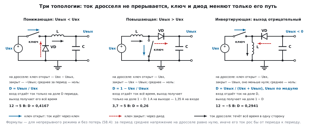
The classic single-switch buck-boost circuit inverts the polarity: from 12 V it gives −5 V. For a positive output from a battery (58.8) you use ICs with four switches: with a high input they work as buck converters, with a low one as boost converters.
In a boost converter the input current is larger than the output current — this follows from conservation of energy, and it is constantly overlooked:
| From 3.7 V we get | Input current at 1 A output |
|---|---|
| 5 V | 1.35 A |
| 12 V | 3.24 A |
| 24 V | 6.49 A |
Stepping up six times draws six times more current from the input. Hence the practical limit of the topology: the battery, traces and switch must withstand not the output current but the input current.
58.2 The inductor: the key component
An inductor is chosen by two numbers: inductance and saturation current.
Inductance sets the current ripple. The common choice is ripple of about 30 % of the load current: less makes the inductor bulky, more increases losses and noise.
For 12 → 5 V, 1 A, 500 kHz: 300 mA of ripple requires 19.4 µH. From the standard series you take 22 µH, which gives 265 mA of ripple.
Saturation current. An inductor is chosen not by the average current but by the peak:
1 A + 265 mA / 2 = 1.133 A, plus a margin of about thirty percent for transients —
1.47 A.
⚠️ Saturation is not "a bit worse". In a saturated inductor the inductance collapses. If it drops to 30 %, the ripple of 265 mA becomes 0.88 A — almost the whole load current, and the switch and inductor overheat within seconds. Symptom: the converter works at light load and "blows up" at full load.
58.3 The output capacitor
The voltage ripple is the sum of two parts:
| Source | At 265 mA of current ripple and 10 µF |
|---|---|
| charging and discharging the capacitance | 6.6 mV |
| internal resistance of 10 mΩ (ceramic) | 2.7 mV |
| together | 9.3 mV — 0.19 % of 5 V |
With an electrolytic capacitor (200 mΩ) the second part alone would give 53 mV — five times worse. That is why switching converters have ceramics on the output, and an electrolytic, if it stays at all, serves as an extra charge reserve.
But the capacitor is not chosen by ripple. The deciding case is a load transient: until the feedback loop reacts (tens of microseconds), the current comes only from the capacitor. A 0.5 A step with a 20 µs response on 10 µF drops the output by 1 V — a hundred times more than the ripple. To keep the dip within 100 mV you need 100 µF.
Hence the rule: the capacitance is calculated from the allowed dip during a load transient, and the ripple is checked afterwards — it will take care of itself.
Ceramic capacitance is not what the reel label says. All the numbers here are calculated from the nominal value, but X5R and X7R ceramics lose capacitance under DC bias (167.3): a "10 µF" 6.3 V part in an 0603 package at 5 V has only a few microfarads. At 5 µF the ripple from recharging and the transient dip double, at 3.3 µF they triple: 3 V instead of 1 V. Calculate with the capacitance from the manufacturer's graph at the operating voltage, and pick a capacitor with a higher voltage rating or a larger package.
58.4 Discontinuous mode
As long as the average current is greater than half the ripple, the inductor current does not stop. The boundary for our example is 133 mA, that is 13 % of the rated load.
Below this boundary the current has time to fall to zero in every period, and the converter behaves differently: the duty cycle no longer equals the voltage ratio, the output tends to rise, and the feedback loop has to cope with it. Good ICs simply switch to burst mode — they produce short bursts of pulses with pauses, saving quiescent current.
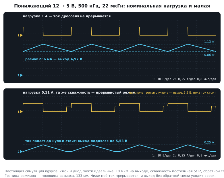
The practical conclusion: a converter must be tested at light load and with no load, not only at rated load. That is where inductor whine (the burst frequency falls into the audible range) and an elevated output voltage show up.
58.5 Where the losses go
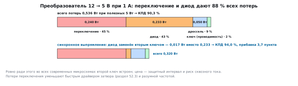
For the same 12 → 5 V converter at 1 A:
| What | Losses | Share |
|---|---|---|
| switching | 0.240 W | 45 % |
| diode | 0.233 W | 43 % |
| inductor | 0.050 W | 9 % |
| switch (conduction) | 0.013 W | 2 % |
| total | 0.536 W | efficiency 90.3 % |
Switching and the diode together account for 88 % of all losses — and both can be fixed.
Synchronous rectification. Replacing the diode with a second switch, you get only 17 mW instead of 0.233 W: efficiency rises to 94.0 %, a gain of 3.7 percentage points. That is exactly why all modern ICs have the second switch built in. The price is the need for dead time (section 57.6) and the risk of shoot-through current.
Switching losses are reduced with a fast gate driver (section 52.3) and a sensible frequency.
58.6 Frequency: what you pay for
Inductance is inversely proportional to frequency:
| Frequency | Inductor for the same ripple |
|---|---|
| 100 kHz | 97.2 µH |
| 500 kHz | 19.4 µH |
| 2 MHz | 4.9 µH |
Between 100 kHz and 2 MHz there is a twentyfold difference in inductance, that is, in inductor size and cost. The temptation to raise the frequency is obvious.
But switching losses grow in direct proportion: at 2 MHz they reach 0.96 W — almost 20 % of the output power, three times more than all the other losses combined. On top of that, layout gets harder and the noise spectrum wider.
The sensible range for powering microcontroller boards is hundreds of kilohertz. Megahertz frequencies are used where board space matters more than efficiency.
58.7 Layout: why the circuit does not always work
A switching converter is the only part of a board where layout affects whether it works at all, not only the noise.
The main loop is the path in which the current changes abruptly: input, switch, diode (or second switch), output capacitor. Its area must be kept to a minimum: every extra centimetre is inductance, and on it a current step produces a voltage spike (section 51.2).
Practical rules:
- input capacitor right next to the switch, not "somewhere near the IC";
- keep the switching node (the "switch — inductor — diode" point) compact: it has the largest voltage swing and it radiates;
- route the feedback path away from the switching node and from the inductor;
- ground as a solid plane, with power and signal ground joined at one point near the IC;
- use a shielded inductor if there are analog circuits nearby.
Symptom of bad layout: it works at low current, whistles or resets at high current; the output "rattles" when an oscilloscope is connected.
58.8 What to choose for a microcontroller board
| Task | Solution |
|---|---|
| 12 → 5 V, up to 0.5 A | a ready-made module or an IC with synchronous rectification |
| 5 → 3.3 V, up to 300 mA | linear: simpler and quieter, but at 300 mA it dissipates 0.51 W — a SOT-223 package or larger, not SOT-23 (section 55.4) |
| from a 3.7 V battery to 3.3 V | a four-switch buck-boost (58.1): the voltage passes through the output value |
| from a battery to 5 V (USB) | boost, calculate the input current |
| powering the analog part | switching + a linear regulator after it (section 53.4) |
And general advice: do not design a converter from scratch if you can use a ready-made IC. The manufacturer has already worked out loop compensation, protection and light-load modes; your job is the inductor, capacitors and layout per the reference design. A fully custom converter makes sense where nothing ready-made exists: non-standard voltages, special requirements, direct control from a microcontroller (section 46.3).
58.9 Pitfalls
Works with no load, heats up under load. The inductor goes into saturation: the peak current is above its rated value.
The inductor whistles. Discontinuous or burst mode at light load — the burst frequency falls into the audible range. Sometimes a minimum load cures it, sometimes it is by design.
The output sags when the load is switched on. Output capacitance is too small: calculate it from the load step, not from the ripple.
Output voltage above nominal with no load. Discontinuous mode.
Noise in the ADC. Interference at the switching frequency: a filter after the converter, a separate linear regulator for the analog part, layout.
The converter resets when an oscilloscope is connected. The ground lead of the probe forms a loop in the main loop — measure with a spring tip instead of the "crocodile" clip.
Everything is calculated correctly, but efficiency is low. A diode instead of synchronous rectification: 43 % of the losses.
At 2 MHz it turned out worse than at 500 kHz. Switching losses grow in proportion to frequency.
58.10 Summary
- The duty cycle is set by the voltage ratio; in a boost converter the input current is larger than the output — six times larger for a sixfold step-up.
- The inductor is calculated from the ripple (30 % of the load current) and chosen by the peak current with a margin: 19.4 µH and 1.47 A for our example.
- Saturation collapses the inductance: 265 mA of ripple turns into 0.88 A.
- Output capacitance is calculated from the dip during a load step (1 V on 10 µF), not from the ripple (9.3 mV) — and from the real capacitance of ceramics at the operating voltage, not from the nominal value.
- Below 13 % of load the mode becomes discontinuous and the simple formulas stop working: test at light load too.
- Losses: switching 45 %, diode 43 %; synchronous rectification gives +3.7 percentage points of efficiency.
- Frequency and inductor size are inversely proportional, but switching losses grow in proportion to frequency.
- The layout of the main loop affects whether the converter works, not only noise.
Next: section 59 "Digital logic: gates and the laws of Boolean algebra" — from the analog part to the digital part that the microcontroller itself is made of.