 Embedded HandbookApps
59. Digital logic: gates and the laws of Boolean algebra
A microcontroller is built entirely from one repeating element — the logic gate. The core, the memory, the timers, the interfaces: all of it is millions of identical little circuits, each of which can do one simple thing.
A programmer does not need to know this right up to the moment when you have to connect external logic to the board, match levels, understand why a signal does not get through, or why a bus does not work at its rated speed. This section is about that minimum.
Terms used in the documentation
Term Meaning logic gate an element that computes one logic function truth table the output listed for every input combination Boolean algebra the algebra of true/false logic values De Morgan's laws rules for moving a negation inside or outside functionally complete basis a gate set from which any function can be built logic level (VIH, VIL, VOH, VOL) logic level, input and output thresholds noise margin how much noise a signal tolerates without an error level shifter, translator a circuit that converts between logic voltages propagation delay (tpd) time from an input change to the output change fan-out how many inputs one output can drive open drain / open collector an output that can only pull the line low wired-AND AND formed by tying open-drain outputs together tri-state, high-Z an output that can disconnect from the line
59.1 Gates and truth tables
A gate takes one or two logic signals and produces one. It is fully described by a truth table — a list of the output for every combination of inputs.
| Input A | Input B | AND | OR | NAND | NOR | XOR |
|---|---|---|---|---|---|---|
| 0 | 0 | 0 | 0 | 1 | 1 | 0 |
| 0 | 1 | 0 | 1 | 1 | 0 | 1 |
| 1 | 0 | 0 | 1 | 1 | 0 | 1 |
| 1 | 1 | 1 | 1 | 0 | 0 | 0 |
Useful observations: AND gives a one on one combination out of four, OR on three, exclusive OR exactly when the inputs differ (hence its role in comparison and in parity calculation).
NOT is the only gate with one input: it inverts the value.
59.2 The laws used in practice
Boolean algebra looks like ordinary algebra but does not match it.
| Law | Expression |
|---|---|
| double negation | ¬¬a = a |
| commutativity | a·b = b·a, a+b = b+a |
| associativity | (a·b)·c = a·(b·c) |
| idempotence | a·a = a, a+a = a |
| absorption | a + a·b = a |
| distributivity of AND over OR | a·(b+c) = a·b + a·c |
| distributivity of OR over AND | a + b·c = (a+b)·(a+c) |
| De Morgan's laws | ¬(a·b) = ¬a + ¬b, ¬(a+b) = ¬a·¬b |
The two highlighted rows are where intuition from arithmetic lets you down.
Distributivity of OR over AND does not exist for ordinary numbers: 2 + 3·4 = 14, while
(2+3)·(2+4) = 30. In logic, though, it holds for all combinations.
De Morgan's laws are the most useful thing to remember. They let you move a negation inside and outside, and in practice they mean this:
if (!(a && b))     эквивалентно     if (!a || !b)
if (!(a || b))     эквивалентно     if (!a && !b)
This is not only about readable conditions: the same rule turns a circuit of AND gates into a circuit of OR gates when the chips at hand are not the right ones.
Checked exhaustively. All the laws above are checked not by an example but on all input combinations — eight combinations for laws with three variables, four for two. This is exactly what sets a truth table apart from reasoning: the enumeration is finite.
59.3 One gate is enough
Any circuit can be built from NAND — it is called a functionally complete basis:
| What we build | How many NANDs |
|---|---|
| NOT | 1 (both inputs tied) |
| AND | 2 |
| OR | 3 |
| exclusive OR | 4 |
The practical meaning: a manufacturer only has to master one element and repeat it millions of times. That is exactly why digital circuits get cheaper with scale, and analog ones do not.
NOR has the same property.
59.4 Levels: where zero ends and one begins
A logic signal is a voltage, and it has four important numbers.
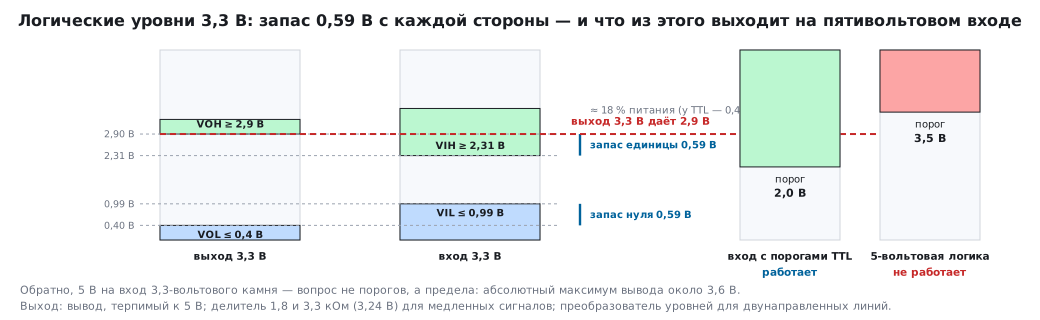
| Symbol | What it means | At a 3.3 V supply |
|---|---|---|
VOH |
what the output guarantees for a one | ≥ 2.9 V |
VIH |
from what voltage the input reads a one | 2.31 V |
VIL |
up to what voltage the input reads a zero | 0.99 V |
VOL |
what the output guarantees for a zero | ≤ 0.4 V |
The difference between what the output delivers and what the input requires is the noise margin: 0.59 V on each side, about 18 % of the supply. That much noise the signal survives without an error.
For comparison, old logic with TTL levels has a margin of only 0.4 V — about one and a half times less. This is one of the reasons modern circuits are more reliable, all else being equal.
59.5 Level matching: 3.3 and 5 volts
The most common practical question, and the answer is different in each direction.
3.3 V into the input of a 5-volt circuit depends on its thresholds:
| Input | One threshold | A 3.3 V output gives 2.9 V |
|---|---|---|
| with TTL thresholds | 2.0 V | works |
| 5-volt logic | 3.5 V | does not work |
This is a trap: a circuit may work with one chip and fail with another that is formally "the same".
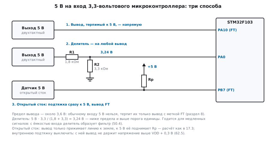
5 V into the input of a 3.3-volt microcontroller is a question not of thresholds but of the maximum voltage. The pin's absolute maximum is about 3.6 V, only 0.3 V of headroom above the supply; 5 V exceeds it, and the pin will be destroyed or start "feeding" the chip through the protection diode. The options:
- a 5 V tolerant pin — on the STM32 these are marked separately; this is the simplest way (section 8);
- a divider — 1.8 kΩ and 3.3 kΩ give 3.24 V: below the limit and above the one threshold. Fine for slow signals; on fast ones the input capacitance and the divider resistance form a filter (section 50.4);
- a level shifter — a chip or a pair of transistors; needed for bidirectional push-pull lines and for I²C on pins that are not 5 V tolerant. On tolerant pins I²C is simpler: the open-drain lines are pulled up straight to 5 V, and the internal pull-up is turned off — with it the pin does not withstand a voltage above VDD + 0.3 V (62.5).
59.6 Delay: why circuits are never instantaneous
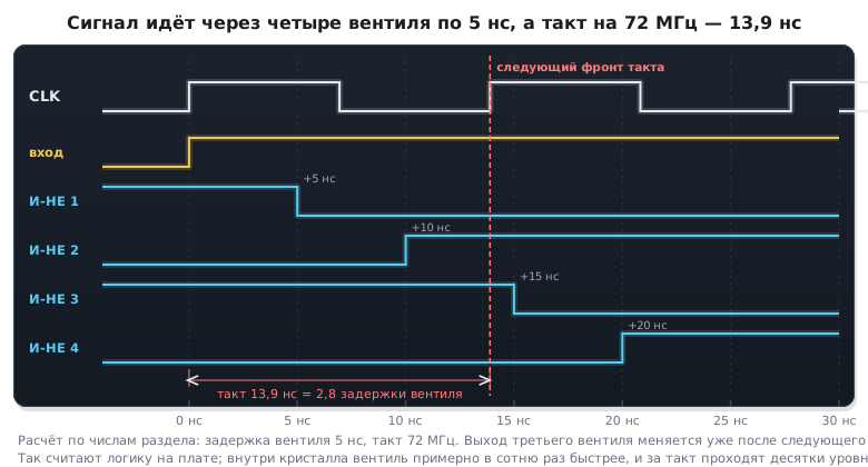
A gate does not switch at once: a discrete logic chip on a board has a typical delay of a few nanoseconds. Delays in a chain add up.
| Circuit depth | Delay (5 ns each) | Maximum frequency |
|---|---|---|
| 2 gates | 10 ns | 100 MHz |
| 4 gates | 20 ns | 50 MHz |
| 10 gates | 50 ns | 20 MHz |
For external logic on a board the calculation is direct: at 72 MHz, within one clock cycle, a signal through 5 ns chips gets through only 2.8 gates in a row — two or three chips in a chain already eat up the cycle.
Inside the die the count is different. 5 ns is the delay of a discrete chip: it has to drive a pin and a trace. A gate inside the die switches in tens of picoseconds, and tens of logic levels fit into one 72 MHz cycle, which is why a Cortex‑M3 does a 32-bit addition in a single cycle. The frequency limit is set by the longest chain between two registers; that chain is what gets cut into pipeline stages — fetch, decode and execute run at the same time for different instructions (section 1).
59.7 Fan-out
A gate output is not made of rubber: every connected input adds capacitance (about 5 pF), and it has to be recharged.
| Inputs on the output | Capacitance | Recharge time at 8 mA |
|---|---|---|
| 1 | 5 pF | 2 ns |
| 10 | 50 pF | 21 ns |
| 20 | 100 pF | 41 ns |
Already at ten inputs the recharge takes four times longer than the gate's own delay: the load becomes the main limit, not the speed of the logic. The cure is buffers — one output feeds several branches, and each branch has its own buffer.
The same calculation explains why a long trace is slower than a short one: a trace is also a capacitance, roughly 1 pF per centimeter.
59.8 Open drain and wired-AND
An ordinary output actively drives the line both high and low — you cannot connect two such outputs: one will pull up, the other down, and both will burn out.
An open-drain output can only pull the line to zero; it is pulled up by a shared pull-up resistor. You can connect as many such outputs as you like: the line is high only if all of them have released it. That is wired-AND — an AND function without a single gate.
This is how I²C (section 17) works, as well as an interrupt line from several sensors and a "fault" signal from several blocks.
The price is speed. The line is pulled up by a resistor, not a transistor, and the rise time is set by RC:
| Pull-up | Line capacitance 50 pF | To the one threshold | Limit |
|---|---|---|---|
| 4.7 kΩ | 235 ns | 283 ns | 1.8 MHz |
| 1 kΩ | 50 ns | 60 ns | 8.3 MHz |
By making the resistor smaller you buy speed with current: at 1 kΩ every output pulling the line to zero sinks 3 mA, and this flows the whole time the line is low.
The third state (tri-state) solves the same problem differently: the output can disconnect completely, and then the line is driven by whoever is active. Memory buses work this way — faster than open drain, but it requires exactly one participant to be active at any moment.
59.9 Pitfalls
The circuit works with one chip and not with "the same" one. Different input thresholds: 2.0 V versus 3.5 V.
A microcontroller pin burned out. 5 V on an input that is not 5 V tolerant.
The signal is distorted on fast edges after a divider. The divider resistance and the input capacitance form a filter.
The logic "glitches" when the power stage is running. The noise exceeded the noise margin: supply decoupling (section 53.5), ground, layout.
The circuit does not work at the design frequency. Add up the gate delays — the sum turned out longer than the period.
The output cannot drive the load. Too many inputs: calculate the capacitance, add a buffer.
I²C works at 100 kHz and does not work at 400 kHz. The pull-up is too large for the line capacitance.
Two outputs were connected — both burned out. Only open-drain or tri-state outputs may be connected together.
An open-drain line "floats" in an undefined state. The pull-up resistor was forgotten: without it nobody forms the one.
59.10 Summary
- A gate is fully described by a truth table; the laws of Boolean algebra are checked by enumerating all combinations, not by an example.
- De Morgan's laws move a negation inside and outside — both in program conditions and in circuits.
- Anything can be built from NAND: NOT from one, AND from two, OR from three, exclusive OR from four.
- The noise margin at 3.3 V is 0.59 V on each side, about 18 % of the supply; old TTL logic had 0.4 V.
- 3.3 V into an input with a TTL threshold works, into the input of 5-volt logic it does not; 5 V into a 3.3 V input requires a 5 V tolerant pin, a divider or a level shifter.
- Delays add up: through 5 ns logic chips at 72 MHz one clock cycle passes 2.8 gates in a row. Inside the die a gate is roughly a hundred times faster, and the core frequency is set by the longest chain between registers.
- Each connected input adds 5 pF; at ten inputs the recharge takes longer than the gate's own delay.
- Open drain gives wired-AND without gates, but the speed is limited by the pull-up: 4.7 kΩ on 50 pF means 1.8 MHz.
Next: section 60 "Multiplexers, decoders, combinational circuits" — what is built from gates when there are many of them.