 Embedded HandbookApps
36к. Signal generators: function, DDS, arbitrary waveform and a generator on STM32
An oscilloscope looks at a signal; a generator creates one. For firmware work it is a way to feed an input with something that is not on the bench yet: a sensor that is not soldered in, a frequency that has to be measured, a sine wave to test a filter. A generator looks like a simple instrument — set the frequency and the amplitude, switch the output on — but it also lies by physics, like the instruments in 36а: the generator screen says 1 V and the probe shows 2 V; a sine built from table points carries extra frequencies next to it; the overshoot on an edge turns out to belong to the cable, not to the generator.
The section goes from the inside to the use: what kinds of generators exist, how direct digital synthesis works (DDS: the frequency is built from a phase counter and a table), where the "50 Ω" comes from, what the sample rate and the filter do in an arbitrary waveform generator, how to read pulse parameters. Then the generator built into the RIGOL DHO900 oscilloscope, with its Bode plot (a curve of gain and phase shift versus frequency), testing firmware with a generator and, finally, your own generator on STM32: a phase accumulator that refills a DMA buffer for the F407 DAC or for F103 PWM.
Sources: DS8626 Rev 9 (STM32F405/407: table 74 — DAC characteristics);
RM0090 Rev 19 (section 14.3.4 — when DAC data reaches the output,
table 42 — DMA1 requests); RM0008 Rev 17 (table 78 — DMA1 requests of
F103); RIGOL DHO900 Datasheet — p. 10 (channel input), 19–21 (Bode Plot and
AFG), 23 (AFG OUT connector), 26 (note on models); DHO900 User Guide —
p. 58 (input impedance), 186–189 (chapter 14, AFG), 194–199 (chapter 15,
Bode Plot); page numbers are those of the PDF files in Books/. The numbers
come from a run of _verify/gen36k: the bench sim36k.c on a PC and the
same source in QEMU on Cortex-M3, independently — ref36k.py (numpy), edges
through a cable — ngspice. The firmware fw36k_f4.c and fw36k_f1.c is
built with -Os and measured; it has not been run on a board.
Terms used in the documentation
Term Meaning function generator a generator of standard waveforms DDS, direct digital synthesis frequency built from a phase counter and a table phase accumulator, tuning word phase register, phase step per sample phase truncation, spur, SFDR dropping low phase bits, spurious component, spurious-free dynamic range AWG, arbitrary waveform generator a generator that plays points from memory image, reconstruction filter mirror copy of the signal around the sample rate, filter after the DAC sinc rolloff, zero-order hold amplitude loss from the DAC steps, holding a sample until the next one output impedance, High Z load source resistance of the output, load setting for a high-impedance input rise time, overshoot, duty cycle edge duration, how far the signal overshoots, fraction of the period at high level sweep, burst changing the frequency over time, a packet of pulses Bode plot, gain / phase margin gain and phase versus frequency, stability margins of a loop update rate, settling time how often the output can change, time to reach the final value
36к.1 Kinds of generators
| kind | how the waveform is made | strong side | weak side |
|---|---|---|---|
| function (analog) | an integrator and a comparator give a triangle and a square, a diode shaper bends the triangle into a sine | smooth tuning, no steps and no images | frequency set by RC and drifts, sine distorted by the shaper |
| DDS | phase counter from a crystal, sine table, DAC | frequency set digitally, crystal accuracy; retuning without a phase jump | truncation spurs and images next to the signal (36к.2, 36к.4) |
| arbitrary waveform (AWG) | point memory, DAC at a set sample rate | any shape: a recorded sensor signal, a pulse with bounce | memory length and sample rate limit both shape and frequency |
| pulse | counters set period, width, delay | edges, width, burst adjusted separately | no sine |
| sweep | frequency changes by a law over a set time | together with an oscilloscope gives the frequency response | a fast sweep distorts the result (36к.7) |
An analog function generator is the same relaxation oscillator that is covered in 179, only with switched capacitors and a sine shaper. Today a bench "function generator" is almost always digital: DDS for sine, square and ramp, and point memory for arbitrary waveforms in one box. Pulse mode and frequency sweep are usually menu items of the same instrument. So the rest of the section is mostly about DDS and points.
36к.2 DDS inside: the phase accumulator and truncation spurs
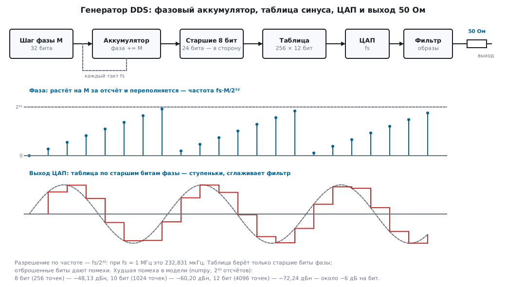
The heart of DDS is a 32-bit phase register. On every tick of the sample rate fs the step M is added to it, and the register overflows — that is the signal period: 2³² is one full turn of phase. The output frequency is
f = M · fs / 2³² M = round(f · 2³² / fs)
The upper phase bits are the point number in the sine table, and the point
goes to the DAC. The frequency step is fs/2³²: at fs = 1 MHz this is
232.831 µHz. An integer step M gives a frequency slightly off the
requested one, but very close (bench sim36k.c, fs = 1 MHz):
| requested | step M | obtained | error |
|---|---|---|---|
| 1 Hz | 4295 | 1.000008 Hz | 8 µHz |
| 1000 Hz | 4294967 | 999.999931 Hz | −69 µHz |
| 1234.56 Hz | 5302395 | 1234.560041 Hz | 41 µHz |
| 10000 Hz | 42949673 | 10000.000009 Hz | 9 µHz |
For comparison, the method of 15.4: a 64-point table, the frequency is
changed by the timer ARR (84 MHz). Near 10 kHz the divider should be
131.25, but it can only be an integer: 131 gives 10019.08 Hz, 132 gives
9943.18 Hz. A 76 Hz step where DDS misses by microhertz. The second
difference: a new DDS frequency is a write of one word M, and the phase
continues from the same place, with no jump; changing the timer ARR
breaks the period.
The price is phase truncation. The table uses only the upper bits
(in our generator 8 of 32, a 256-point table), and the lower 24 are dropped.
The phase error repeats periodically, and spurious components grow in the
spectrum next to the signal. Model ref36k.py: a spectrum of 2²⁰
samples, the step M is a multiple of 2¹² (then the sequence is exactly
periodic and the spectrum lands exactly on the bins), 24 values of M are
tried, the table holds an exact sine:
| phase bits into the table | points | worst spur (model) | estimate −6.02 dB per bit |
|---|---|---|---|
| 8 | 256 | −48.13 dBc | −48.16 dBc |
| 10 | 1024 | −60.20 dBc | −60.20 dBc |
| 12 | 4096 | −72.24 dBc | −72.24 dBc |
(dBc means decibels relative to the carrier, that is, the signal itself.) Every phase bit is about 6 dB. With the real table of our generator — 12-bit codes — the worst spur is the same: −48.13 dBc; it is set by phase truncation, not by the DAC resolution. To bring the spurs down to −72.24 dBc, the table needs 4096 points — 8 KB of flash memory instead of 512 bytes.
36к.3 The 50 Ω output: one value on the generator screen, twice as much on the probe
Inside the generator there is an EMF source with a 50 Ω resistor in
series. The generator does not know what is connected, and by default
assumes the load is also 50 Ω: then exactly half of the EMF appears on it,
and that half is what it shows on the screen. "1 Vpp" set means 2 V
peak-to-peak of EMF. What appears on different loads (ref36k.py, divider
50 Ω / load):
| load | across it, with "1 Vpp" on the screen |
|---|---|
| 50 Ω | 1.0000 V |
| 100 Ω | 1.3333 V |
| 1 kΩ | 1.9048 V |
| 10 kΩ | 1.9900 V |
| 1 MΩ (oscilloscope input) | 1.9999 V |
An oscilloscope input and a microcontroller input are high-impedance, and they get twice what is written. This is not an instrument fault: the output menu of the generator has a load setting (50 Ω or High Z), and it changes only the conversion of the number on the screen, not the signal itself. In radio engineering power is counted into 50 Ω: 0 dBm is 1 mW, 0.2236 V RMS, or 0.6325 V peak-to-peak of a sine.
Where it hits the firmware. You need a 0…3.3 V signal on an ADC pin. The output mode stayed at "50 Ω", 3.3 Vpp with a 1.65 V offset is set — the screen promises 0…3.30 V, but the high-impedance pin gets 0…6.60 V: above anything a 3.3-volt pin tolerates. The right way is either to switch the load to High Z, or in "50 Ω" mode to set 1.650 Vpp and a 0.825 V offset: the pin then gets 0…3.30 V.
The output impedance of your generator can be checked in a minute: the amplitude with no load (on the oscilloscope input) and with a 51 Ω resistor. R = Rload · (Uopen / Uload − 1); for 2.00 V and 1.01 V on 51 Ω this gives 49.99 Ω.
The DHO900 oscilloscope has only a 1 MΩ ± 1 % and 15 pF ± 3 pF input (Datasheet, p. 10; User Guide, p. 58 — there are no other input modes). To look at a fast generator on a matched load, an external 50 Ω feed-through termination is put on the input. The output impedance of its own AFG generator and the load for which the 2 mV…10 V amplitude is given are not stated in the documents (Datasheet, p. 20) — measure them with the method above.
36к.4 Arbitrary waveform generator: sample rate, images, sinc
The DAC holds each sample until the next one — the output is made of
steps. The steps have their own spectrum: the signal f repeats around the
sample rate and its multiples — at fs − f, fs + f, 2fs − f… These copies are
called images. In addition, the step itself attenuates everything by
the law sinc(f/fs) = sin(π·f/fs)/(π·f/fs) — the closer to fs, the stronger
(ref36k.py, formula):
| f / fs | signal | image at fs − f | image relative to the signal |
|---|---|---|---|
| 0.10 | −0.14 dB | −19.23 dB | −19.08 dB |
| 0.25 | −0.91 dB | −10.45 dB | −9.54 dB |
| 0.40 | −2.42 dB | −5.94 dB | −3.52 dB |
| 0.50 | −3.92 dB | −3.92 dB | 0.00 dB |
The numerical model — steps of 64 sub-samples per sample and a spectrum — gave the same numbers within 0.01 dB. Conclusion: ten samples per period (f/fs = 0.1) is not yet a "clean sine" but a sine with an image at −19 dB. A reconstruction filter after the DAC removes the images. Example: fs = 1 MHz, signal up to 100 kHz, image at 900 kHz, −60 dBc needed. A Butterworth filter with a 200 kHz cutoff:
| order | attenuation at 900 kHz | resulting image | droop at 100 kHz |
|---|---|---|---|
| 3 | 39.19 dB | −58.28 dBc | 0.067 dB |
| 4 | 52.26 dB | −71.34 dBc | 0.017 dB |
The fourth order (178 — how to build it with op-amps) solves the task, and the sinc droop at 100 kHz — 0.143 dB — can be corrected in the table itself if needed.
Table length. If a table of L points is output one point per sample
(as in 15.4), the first extra harmonics sit at (L − 1)·f and (L + 1)·f, and
the first one is weaker than the signal exactly L − 1 times (ref36k.py,
spectrum against the formula):
| points L | first extra | level |
|---|---|---|
| 16 | 15·f | −23.52 dB |
| 32 | 31·f | −29.82 dB |
| 64 | 63·f | −35.98 dB |
| 256 | 255·f | −48.13 dB |
For the generator of 15.4 (64 points of 10 µs, 1562.5 Hz) this is a component at 98.4375 kHz at −35.98 dB — the filter removes it. The 256-point row gave the same −48.13 dB as the worst truncation spur in 36к.2: it is the same table staircase seen from two sides.
Two kinds of arbitrary waveform generator. In the "true" one each memory point is output exactly once, and the frequency is changed by the sample rate — the shape is kept exactly. In the phase-accumulator kind the sample rate is fixed, and points are skipped or repeated — short details of the shape jitter. An example from the DHO900 numbers: memory up to 16 kpts, 156 MSa/s, arbitrary waveform frequency up to 10 MHz (Datasheet, p. 19–20). Each of the 16384 points at 156 MSa/s can be output only up to 9521.48 Hz; above that, points are inevitably skipped. Which kind is inside is not stated in the documents; this is a conclusion from the arithmetic.
36к.5 Square waves and pulses: edge, overshoot, duty cycle
Three numbers describe a pulse: the rise time (from 10 to 90 % of the amplitude), the overshoot (by how many percent the signal flies past the settled level) and the duty cycle (the fraction of the period at high level). How the oscilloscope bandwidth stretches an edge — 36а.3; automatic measurements of these values — 36е.
The overshoot on the screen often belongs to the wires, not to the
generator. ngspice model (edge36k.cir): EMF 0 → 2 V with an 8 ns edge
(10…90 %), a 1 m cable — 50 Ω and 5 ns, at the end an oscilloscope input
of 1 MΩ and 15 pF — like the DHO900:
| source and load | level | peak | overshoot | rise time 10…90 % |
|---|---|---|---|---|
| generator 50 Ω → input 1 MΩ | 1.9999 V | 1.9999 V | none | 8.08 ns |
| generator 50 Ω → load 50 Ω | 1.0000 V | 1.0000 V | none | 8.01 ns |
| source 10 Ω → input 1 MΩ | 1.9999 V | 3.31 V | 65.5 % | 4.95 ns |
A 50 Ω generator on an unloaded cable works cleanly: the wave reflected from the open end comes back and is absorbed in its own 50 Ω. A low-impedance source — a chip pin — on the same metre of cable gives an overshoot of two thirds of the amplitude: the reflection goes back and rings. Hence the bench rule: a fast signal from a pin to the oscilloscope goes through a short probe, not through a cable.
"Skvazhnost" and duty cycle. In Russian technical literature "skvazhnost" is the ratio of the period to the pulse width, T/τ; it is always greater than one. A generator menu says Duty — that is the inverse value, the fraction of the period:
| Duty | duty cycle as a fraction | "skvazhnost" T/τ |
|---|---|---|
| 50 % | 0.50 | 2 |
| 20 % | 0.20 | 5 |
| 10 % | 0.10 | 10 |
| 1 % | 0.01 | 100 |
In this handbook, as in everyday speech, "skvazhnost" often means exactly the fraction of the period (57ж, 13.5) — when reading someone else's specification, check which one is meant.
A square wave from DDS jitters by one sample. If the square wave is made by comparing the phase with a threshold, an edge can only sit on a sample. Bench: 3 kHz at fs = 1 MHz, one second of samples — exactly 3000 periods, but each period is either 333 or 334 samples, the pulse 166 or 167. The edges jump by 1 µs, the average frequency is exact. That is why good generators make the square wave with a comparator from a filtered sine: the DHO900 specifies 500 ps jitter with a sample step of 6.41 ns (Datasheet, p. 20).
36к.6 The generator in the oscilloscope: AFG and Bode plot on the DHO900
The DHO914S and DHO924S models have a single-channel AFG generator and a Bode plot mode built into the oscilloscope (Datasheet, p. 26, note 7; User Guide, p. 186). The output is the BNC connector [AFG OUT] on the rear panel (Datasheet, p. 23). What it can do according to the datasheet — all numbers are marked there as typical (Datasheet, p. 19–21):
| parameter | value |
|---|---|
| samples and resolution | 156 MSa/s, 14 bits |
| waveforms | Sine, Square, Ramp, DC, Noise and user-defined (Arb) |
| Sine | 2 mHz…25 MHz, flatness ±0.5 dB relative to 1 kHz, harmonics −40 dBc, THD < 1 % |
| Square | 2 mHz…15 MHz, edge < 15 ns, overshoot < 5 %, Duty 1…99 % |
| Ramp | 2 mHz…150 kHz, symmetry 0…100 % |
| Arb | 2 mHz…10 MHz, 2 points…16 kpts |
| amplitude | 2 mV…10 V up to 10 MHz, 2 mV…5 V above |
| offset | −5…5 V |
| frequency accuracy | 100 ppm |
| modulation | AM, FM, PM, internal, modulation frequency 2 mHz…1 MHz |
100 ppm is ±0.1 Hz at 1 kHz: when testing a firmware timer with a crystal, such a generator may itself be less accurate than the board. Measure the frequency with a frequency counter rather than trusting the generator dial.
How to switch it on (User Guide, p. 186–189): the AFG key on the front panel or the AFG label at the bottom of the screen turns the output on, a second press opens the menu. The menu has Function (waveform), Frequency, Amplitude, Offset, Phase, Duty for the square wave, Symm for the ramp and the Output switch. The generator and the oscilloscope share one box, so the shield of the AFG OUT connector is most likely tied to the same ground as the probes (36а.5); the documents do not say this directly — check it with a continuity tester before feeding a board with a "floating" ground.
Bode plot (User Guide, p. 194–199). The instrument sweeps the generator sine in frequency and at each frequency compares two channels: In — the signal at the circuit input, Out — at the output. The result is gain and phase curves, a cursor with Freq, Gain and Phase, and the PM and GM margins for a feedback loop. The settings are in the Bode Plots menu: In and Out (channels CH1–CH4), Sweep Type (Log or Line), Start Freq from 10 Hz to 24.99 MHz, Stop Freq from 100 Hz to 25 MHz, the number of points from 10 to 300 (default 10), Amp — amplitude from 20 mV to 5 V, Var.Amp — a different amplitude in different frequency ranges; Display Type — Wave or Chart; saving to csv or html. The datasheet calls the number of points "per octave" (p. 19), the guide "per decade" (p. 199): check how many points your instrument actually produces.
The connection diagram the instrument shows with the Tips button is for a switching supply loop: an isolation transformer and an injection resistor in the feedback path (User Guide, p. 198). For an ordinary filter it is simpler: AFG OUT to the filter input and CH1 (In) there too, the filter output to CH2 (Out). Gain is computed as the ratio of Out to In, so neither the generator output impedance nor cable losses enter the result.
Example — the RC filter of the F103 generator from 36к.8 (1 kΩ and 10 nF,
then 10 kΩ and 1 nF). Start Freq 100 Hz, Stop Freq 1 MHz, 10 points per
decade — 41 points. What the curve should look like (ref36k.py):
| frequency | gain | phase |
|---|---|---|
| 1 kHz | −0.04 dB | −7.5° |
| 5 kHz | −0.96 dB | −36.2° |
| 9561 Hz | −3 dB | −63.1° |
| 100 kHz | −32.19 dB | −161.1° |
| 1 MHz | −71.93 dB | −178.1° |
At 1 MHz only 0.253 mV of the 1 V amplitude remains at the output — that is already at the channel noise level, and the curve will scatter there; the guide warns directly that the mode does not suit noisy circuits (User Guide, p. 195). Var.Amp helps: a larger amplitude at high frequencies. Or end the sweep at 100 kHz, where the output still has 24.6 mV.
36к.7 A generator tests the firmware
A sensor that does not exist yet. An analog sensor with a 0.3…3.0 V output is, for the generator, an amplitude of 2.70 V and an offset of 1.65 V with the High Z load, or 1.350 Vpp and 0.825 V if the output stayed in "50 Ω" mode (36к.3). A slow ramp checks the conversion of the ADC code into a value over the whole scale (ADC errors — 14а), a sine checks filtering, Noise checks thresholds and hysteresis. Pulses of a set frequency replace a flow sensor or a tachometer on a timer capture input (13.6); a burst of N pulses checks that the counter neither loses nor adds edges.
PWM signals. A servo signal is a 20 ms period with a 1.5 ms pulse, that is Duty 7.5 %. Firmware that measures it by capture with a 1 µs timer tick resolves 0.005 % of the period — much finer than the Duty setting step of most generators. So it is more convenient to test the firmware by pulse width (Pulse mode) rather than by percent.
Frequency response of a filter in firmware. The chain: generator → ADC pin → filter in firmware → DAC (F407, 36к.8) → oscilloscope. The filter is one IIR stage (81а.3), y += (x − y)/16 at 10 kHz sampling: cutoff 102.75 Hz (the approximate formula −ln(1 − 1/16)·fs/2π gives 102.72 Hz), −3.01 dB there. The DHO900 Bode plot draws such a curve by itself: In — on the ADC pin, Out — on the DAC output, Start Freq 10 Hz, Stop Freq 4 kHz — below half the sample rate, 5000 Hz. One detail: in the Bode Plots menu the sine has an amplitude but no offset (User Guide, p. 199), and an ADC pin does not tolerate negative voltage. A bias network is needed: a 10 µF capacitor and a 20 kΩ / 20 kΩ divider from 3.3 V — midpoint 1.65 V, cutoff 1.59 Hz, loss at 10 Hz 0.109 dB.
Sweep slowly. A filter does not respond to a frequency change at once —
our stage has a time constant 1/(2π·fc) = 1.549 ms. Model ref36k.py: a
continuous logarithmic sweep 10 Hz → 1 kHz, gain at the cutoff from the
output envelope:
| sweep time | gain at 102.75 Hz | correct |
|---|---|---|
| 0.05 s | −1.78 dB | −3.01 dB |
| 0.2 s | −2.70 dB | −3.01 dB |
| 1 s | −2.93 dB | −3.01 dB |
| 5 s | −2.99 dB | −3.01 dB |
A fast sweep shows the filter "wider" than it is: the output still remembers the lower frequency. How long the DHO900 Bode plot waits at each point is not stated in the documents — check that the curve does not change with twice the number of points. How to read amplitude and phase response — 50а, analog filters in front of an ADC — 178.
36к.8 A generator on STM32: phase accumulator in an interrupt and in DMA
A table generator on the DAC is already built in 15.4: timer TIM6 triggers
the DAC, DMA cycles the table, frequency = trigger rate / number of points.
The DAC's built-in triangle and noise — 15.5, a phase accumulator in audio —
198л and 198п. What is new here is DDS on top of the same chain: frequency in
microhertz steps and without a phase jump. The common logic is dds36k.c,
one for F407 and F103; its heart is the fill loop:
        while (n--) {
            *buf++ = (uint16_t)(dds_sine[ph >> (32u - DDS_TAB_BITS)] >> sh);
            ph += w;
        }
F407, DAC and DMA. TIM6 counts 84 MHz / 84 — the DAC is triggered 1 million times per second, exactly the limit from table 74 of DS8626 (1 MS/s). DMA1 Stream5, channel 7 — the DAC1 request (table 42 of RM0090) — cycles a buffer of two halves of 256 samples. At the middle and at the end of the buffer an interrupt comes, and the handler fills the half that DMA has just passed:
void gen_set(uint32_t f_centihz)
{
    gen.word = dds_word(f_centihz, FS_HZ);
}

#ifndef DDS_IRQ
void DMA1_Stream5_IRQHandler(void)
{
    uint32_t isr = DMA1->HISR;
    if (isr & DMA_HISR_HTIF5) {            /* DMA ушёл во вторую половину — первая свободна */
        DMA1->HIFCR = DMA_HIFCR_CHTIF5;
        dds_fill(&gen, buf, HALF);
    }
    if (isr & DMA_HISR_TCIF5) {            /* DMA вернулся в начало — свободна вторая */
        DMA1->HIFCR = DMA_HIFCR_CTCIF5;
        dds_fill(&gen, buf + HALF, HALF);
    }
}
The sample reaches the pin three APB1 clock cycles after the timer trigger — a constant delay, the samples go evenly (RM0090, 14.3.4). The handler comes once every 256 µs and does not have to make it "by the sample" — only within 256 µs.
F407, sample in a timer interrupt (-DDDS_IRQ) — a variant without
DMA, simpler to understand and to debug:
void TIM6_DAC_IRQHandler(void)
{
    TIM6->SR = 0u;
    DAC->DHR12R1 = dds_next(&gen);         /* без запуска ЦАП берёт значение через такт APB1 */
}
Without a hardware trigger the DAC moves the value to the output one APB1 clock cycle after the write (RM0090, 14.3.4) — that is, at the moment the handler gets there. Any other interrupt with a higher priority shifts the sample, and the sine jitters in time. So the interrupt is for low sample rates, DMA for everything else.
F103 without a DAC: PWM and an RC filter. The F103C8 has no DAC (15.1).
TIM2 gives PWM on PA0 with ARR = 255 — 8 bits, 72 MHz / 256 = 281250 Hz,
which is also the sample rate. The TIM2_UP request — DMA1 Channel 2 (table 78
of RM0008) — puts the next sample into CCR1 on every update, and the
CCR1 preload applies it from the start of the next period. The same
dds_fill, a shift by 4 bits — codes 0…255. PWM resolution and frequency
trade places:
| PWM bits | PWM frequency = sample rate | step at 3.3 V |
|---|---|---|
| 8 | 281250 Hz | 12.94 mV |
| 10 | 70312.5 Hz | 3.23 mV |
| 12 | 17578.125 Hz | 0.81 mV |
The filter is two RC sections: 1 kΩ and 10 nF, then 10 kΩ and 1 nF (the second ten times higher in impedance, so that it loads the first one less). The −3 dB cutoff is 9561 Hz, the loss at 1 kHz is 0.04 dB, at 5 kHz 0.96 dB; the 281250 Hz carrier is attenuated by 49.92 dB, and the ripple at half duty is 13.00 mV peak-to-peak, about one 8-bit step. The useful band of such a generator is up to a few kilohertz; the same curve can be taken with a Bode plot (36к.6).
Sizes (arm-none-eabi-gcc 12.2.1, -Os -Wall -Wextra -Werror):
| variant | own firmware | dds36k.o |
flash image | RAM |
|---|---|---|---|---|
| F407, DAC + DMA | 356 bytes | 656 bytes | 2108 bytes | 1040 bytes |
| F407, sample in interrupt | 260 bytes | 656 bytes | 1908 bytes | 16 bytes |
| F103, PWM + DMA | 320 bytes | 656 bytes | 1908 bytes | 528 bytes |
Of the 656 bytes of dds36k.o the sine table takes 512, dds_fill — 100,
dds_word — 26. An unexpected line in the memory map is __udivmoddi4,
700 bytes on F407 and 702 on F103: this is the 64-bit division in
dds_word, and the library pulls it in whole. If the frequency is set once,
compute the step in advance, as a constant.
What it costs the CPU. The body of the sine loop on F407 after -Os is
seven instructions per sample (disassembler):
lsrs    r7, r6, #24
add r6, r5
ldrh.w  r7, [lr, r7, lsl #1]
asr.w   r7, r7, ip
strh.w  r7, [r1], #2
subs    r4, #1
bcs.n   80002dc <dds_fill+0x40>
A lower-bound estimate, at one cycle per instruction: 1 million samples per second is 7 million cycles of 168 million, about 4.2 % of the F407 core; on F103 at 281250 samples it is 2.7 % of 72 MHz. The interrupt variant: 16 handler instructions plus 12 cycles of entry (7а.5) and about as many for exit — about 40 cycles: at 100 kHz this is 2.4 % of the core, at 1 MHz it would be 24 %. Flash wait states add to these figures — they were not measured on hardware.
Frequency limits on F407:
- the frequency step is fs/2³² = 232.831 µHz (on F103 at 281250 Hz — 65.484 µHz);
- above half of fs (500 kHz) there is no signal at all, and a clean sine goes up to about fs/10 = 100 kHz with a fourth-order filter (36к.4);
- DAC: table 74 promises 1 MS/s for a step of one code unit, while it covers the full scale in 3 µs typical and 6 µs maximum (CLOAD ≤ 50 pF, RLOAD ≥ 5 kΩ). If the full scale is assumed to be covered linearly, this is 1.10 V/µs and 0.55 V/µs — a full-swing sine keeps up to about 106.1 kHz and 53.1 kHz. At 10 kHz the step between samples is 128.6 codes, at 100 kHz 1286.5 codes: far from "one unit".
36к.9 Pitfalls
Twice as much on the probe as on the generator screen. The output is designed for 50 Ω and the load is high-impedance: with "1 Vpp" the oscilloscope input gets 1.9999 V (36к.3). Switch the load to High Z — or remember the ×2.
The ADC pin got 6.6 V. The same effect with offset: 3.3 Vpp and 1.65 V in "50 Ω" mode — 0…6.60 V on a high-impedance pin. Look at the generator output with an oscilloscope before connecting it to the board.
A "clean" sine with extra frequencies next to it. DDS phase truncation: a 256-point table — spurs up to −48.13 dBc; 4096 points — up to −72.24 dBc (36к.2).
A sine of 10 points per period with an image at −19 dB. DAC steps: the image at fs − f relative to the signal is −19.08 dB at f = fs/10. A reconstruction filter is needed (36к.4).
65.5 % overshoot on the edge. A low-impedance source on an unmatched cable (36к.5). A 50 Ω generator on the same cable gives no overshoot.
Duty 20 % written in a specification as "skvazhnost 20 %". In Russian, "skvazhnost" is T/τ: at Duty 20 % it equals 5 (36к.5).
A square wave from a table jitters. The edge is tied to a sample: at 1 MHz — jumps of 1 µs, periods of 333 and 334 samples (36к.5).
The Bode plot scatters at high frequencies. The signal at the filter output went into noise: at 1 MHz the RC filter gives 0.253 mV per 1 V. Var.Amp or a lower sweep end (36к.6).
The firmware filter response is "wider" than calculated. The sweep is faster than the filter time constant: 0.05 s for two decades showed −1.78 dB instead of −3.01 dB at the cutoff (36к.7).
The generator firmware is bigger than expected. The 64-bit division in the phase step pulled in 700 bytes of library code (36к.8).
The sine from an interrupt jitters while UART is working. The sample
reaches the output at the moment of the DHR12R1 write, and other
interrupts shift the handler. Trigger the DAC from a timer and use DMA
(36к.8).
36к.10 Summary
- A bench generator today is DDS plus point memory; the analog function generator remains in circuits like 179.
- DDS: f = M·fs/2³², frequency step fs/2³² (232.831 µHz at 1 MHz), retuning without a phase jump. Phase truncation is about −6 dB per bit: 256 points — −48.13 dBc.
- 50 Ω output: the screen shows the voltage on a 50-ohm load; a high-impedance load gets twice as much. The High Z setting changes the number, not the signal.
- DAC steps: sinc droop and images at fs ± f; at fs/10 the image is −19.08 dB, a fourth-order filter brings it to −71.34 dBc.
- Overshoot on an edge often comes from the cable and matching, not from the generator; "skvazhnost" T/τ is not the same as Duty.
- DHO914S/DHO924S: a generator up to 25 MHz and a Bode plot; gain is computed as Out/In, so the generator output does not enter the result. There is no offset in Bode mode — an ADC pin needs a bias network.
- A generator tests firmware: it replaces a sensor, sets PWM, takes the frequency response of a filter — if the sweep is slower than the filter responds.
- Your own generator on STM32: a phase accumulator refills halves of a DMA buffer — F407 with a DAC up to 1 MS/s, F103 through 281250 Hz PWM and two RC sections. The code is 656 bytes of common logic and 260…356 bytes of own firmware.
Full sources
dds36k.h — phase accumulator: structure, step, sample for the interrupt.
/* dds36k.h — раздел 36к: прямой цифровой синтез (DDS) для генератора на STM32.
 * Общая логика для ЦАП F407 и ШИМ F103, на компьютере и в QEMU — одна и та же. */
#ifndef DDS36K_H
#define DDS36K_H
#include <stdint.h>

#define DDS_TAB_BITS 8u                     /* 256 точек синуса: старшие 8 бит фазы */
#define DDS_TAB_LEN  (1u << DDS_TAB_BITS)
#define DDS_FULL     4095u                  /* 12 бит, полная шкала ЦАП */

extern const uint16_t dds_sine[DDS_TAB_LEN];

typedef struct {
    uint32_t phase;   /* фазовый аккумулятор: 2^32 — один период */
    uint32_t word;    /* шаг фазы за отсчёт (tuning word) */
    uint32_t duty;    /* 0 — синус; иначе меандр: 1, пока phase < duty */
    uint8_t  shift;   /* сдвиг отсчёта вправо: 0 — 12 бит для ЦАП, 4 — 8 бит для ШИМ */
} dds_t;

/* Шаг для частоты f (в сотых долях герца) при частоте отсчётов fs, с округлением. */
uint32_t dds_word(uint32_t f_centihz, uint32_t fs_hz);
/* Порог фазы для меандра: доля периода в десятых процента (500 — 50 %). */
uint32_t dds_duty(uint32_t permille);
/* n следующих отсчётов в buf; фаза продолжается с того места, где кончился прошлый вызов. */
void dds_fill(dds_t *d, uint16_t *buf, uint32_t n);

/* Один отсчёт синуса — для варианта «в прерывании таймера». */
static inline uint16_t dds_next(dds_t *d)
{
    uint16_t v = (uint16_t)(dds_sine[d->phase >> (32u - DDS_TAB_BITS)] >> d->shift);
    d->phase += d->word;
    return v;
}
#endif
dds36k.c — sine table, phase step, square-wave threshold and buffer fill.
/* dds36k.c — раздел 36к: шаг фазы, порог меандра и заполнение буфера отсчётами. */
#include "dds36k.h"

/* round(2048 + 2047 * sin(2 * pi * k / 256)), k = 0…255 */
const uint16_t dds_sine[DDS_TAB_LEN] = {
    2048, 2098, 2148, 2199, 2249, 2299, 2348, 2398, 2447, 2497, 2545, 2594, 2642, 2690, 2738, 2785,
    2831, 2878, 2923, 2968, 3013, 3057, 3100, 3143, 3185, 3227, 3267, 3307, 3347, 3385, 3423, 3459,
    3495, 3531, 3565, 3598, 3630, 3662, 3692, 3722, 3750, 3777, 3804, 3829, 3853, 3876, 3898, 3919,
    3939, 3958, 3975, 3992, 4007, 4021, 4034, 4045, 4056, 4065, 4073, 4080, 4085, 4089, 4093, 4094,
    4095, 4094, 4093, 4089, 4085, 4080, 4073, 4065, 4056, 4045, 4034, 4021, 4007, 3992, 3975, 3958,
    3939, 3919, 3898, 3876, 3853, 3829, 3804, 3777, 3750, 3722, 3692, 3662, 3630, 3598, 3565, 3531,
    3495, 3459, 3423, 3385, 3347, 3307, 3267, 3227, 3185, 3143, 3100, 3057, 3013, 2968, 2923, 2878,
    2831, 2785, 2738, 2690, 2642, 2594, 2545, 2497, 2447, 2398, 2348, 2299, 2249, 2199, 2148, 2098,
    2048, 1998, 1948, 1897, 1847, 1797, 1748, 1698, 1649, 1599, 1551, 1502, 1454, 1406, 1358, 1311,
    1265, 1218, 1173, 1128, 1083, 1039,  996,  953,  911,  869,  829,  789,  749,  711,  673,  637,
     601,  565,  531,  498,  466,  434,  404,  374,  346,  319,  292,  267,  243,  220,  198,  177,
     157,  138,  121,  104,   89,   75,   62,   51,   40,   31,   23,   16,   11,    7,    3,    2,
       1,    2,    3,    7,   11,   16,   23,   31,   40,   51,   62,   75,   89,  104,  121,  138,
     157,  177,  198,  220,  243,  267,  292,  319,  346,  374,  404,  434,  466,  498,  531,  565,
     601,  637,  673,  711,  749,  789,  829,  869,  911,  953,  996, 1039, 1083, 1128, 1173, 1218,
    1265, 1311, 1358, 1406, 1454, 1502, 1551, 1599, 1649, 1698, 1748, 1797, 1847, 1897, 1948, 1998,
};

uint32_t dds_word(uint32_t f_centihz, uint32_t fs_hz)
{
    uint64_t den = (uint64_t)fs_hz * 100u;            /* fs в сотых долях герца */
    return (uint32_t)((((uint64_t)f_centihz << 32) + den / 2u) / den);
}

uint32_t dds_duty(uint32_t permille)
{
    return (uint32_t)(((uint64_t)permille << 32) / 1000u);
}

void dds_fill(dds_t *d, uint16_t *buf, uint32_t n)
{
    uint32_t ph = d->phase;
    const uint32_t w = d->word;
    const uint8_t sh = d->shift;
    if (d->duty != 0u) {                               /* меандр: сравнение фазы с порогом */
        const uint32_t duty = d->duty;
        const uint16_t hi = (uint16_t)(DDS_FULL >> sh);
        while (n--) {
            *buf++ = ph < duty ? hi : 0u;
            ph += w;
        }
    } else {                                           /* синус: старшие 8 бит фазы — номер точки */
        while (n--) {
            *buf++ = (uint16_t)(dds_sine[ph >> (32u - DDS_TAB_BITS)] >> sh);
            ph += w;
        }
    }
    d->phase = ph;
}
fw36k_f4.c — F407: DAC + DMA or a sample in the TIM6 interrupt.
/* fw36k_f4.c — раздел 36к: генератор DDS на STM32F407, выход ЦАП PA4.
 * Основной вариант: TIM6 запускает ЦАП миллион раз в секунду, DMA1 Stream5 по кругу гонит буфер
 * из двух половин в DHR12R1 (связка из 15.4), а прерывание DMA дописывает освободившуюся половину
 * отсчётами из фазового аккумулятора. Вариант -DDDS_IRQ: без DMA, один отсчёт в прерывании TIM6
 * сто тысяч раз в секунду. Такт: HSE 8 МГц -> PLL 168 МГц, APB1 42 МГц, таймеры APB1 — 84 МГц. */
#include "stm32f4xx.h"
#include "dds36k.h"

#ifndef DDS_IRQ
#define FS_HZ   1000000u                   /* 84 МГц / 84 */
#define HALF    256u                       /* отсчётов в половине буфера: прерывание раз в 256 мкс */
static uint16_t buf[2u * HALF];
#else
#define FS_HZ   100000u                    /* 84 МГц / 840 */
#endif

static dds_t gen;

/* Частота меняется на ходу: шаг — одно 32-битное слово, запись неделимая. */
void gen_set(uint32_t f_centihz)
{
    gen.word = dds_word(f_centihz, FS_HZ);
}

#ifndef DDS_IRQ
void DMA1_Stream5_IRQHandler(void)
{
    uint32_t isr = DMA1->HISR;
    if (isr & DMA_HISR_HTIF5) {            /* DMA ушёл во вторую половину — первая свободна */
        DMA1->HIFCR = DMA_HIFCR_CHTIF5;
        dds_fill(&gen, buf, HALF);
    }
    if (isr & DMA_HISR_TCIF5) {            /* DMA вернулся в начало — свободна вторая */
        DMA1->HIFCR = DMA_HIFCR_CTCIF5;
        dds_fill(&gen, buf + HALF, HALF);
    }
}
#else
void TIM6_DAC_IRQHandler(void)
{
    TIM6->SR = 0u;
    DAC->DHR12R1 = dds_next(&gen);         /* без запуска ЦАП берёт значение через такт APB1 */
}
#endif

static void clock_168(void)
{
    RCC->CR |= RCC_CR_HSEON;
    while (!(RCC->CR & RCC_CR_HSERDY)) {
    }
    FLASH->ACR = FLASH_ACR_ICEN | FLASH_ACR_DCEN | FLASH_ACR_PRFTEN | FLASH_ACR_LATENCY_5WS;
    RCC->PLLCFGR = (8u << RCC_PLLCFGR_PLLM_Pos) | (336u << RCC_PLLCFGR_PLLN_Pos)
                 | RCC_PLLCFGR_PLLSRC_HSE | (7u << RCC_PLLCFGR_PLLQ_Pos);      /* PLLP = 2 */
    RCC->CFGR = RCC_CFGR_PPRE1_DIV4 | RCC_CFGR_PPRE2_DIV2;
    RCC->CR |= RCC_CR_PLLON;
    while (!(RCC->CR & RCC_CR_PLLRDY)) {
    }
    RCC->CFGR |= RCC_CFGR_SW_PLL;
    while ((RCC->CFGR & RCC_CFGR_SWS) != RCC_CFGR_SWS_PLL) {
    }
}

int main(void)
{
    clock_168();
    RCC->AHB1ENR |= RCC_AHB1ENR_GPIOAEN | RCC_AHB1ENR_DMA1EN;
    RCC->APB1ENR |= RCC_APB1ENR_DACEN | RCC_APB1ENR_TIM6EN;
    GPIOA->MODER |= GPIO_MODER_MODER4;     /* PA4 — аналоговый */
    gen.shift = 0u;
    gen_set(100000u);                      /* 1000,00 Гц */
    TIM6->PSC = 0u;
    TIM6->ARR = 84000000u / FS_HZ - 1u;
#ifndef DDS_IRQ
    dds_fill(&gen, buf, 2u * HALF);        /* обе половины готовы до первого запуска */
    DMA1_Stream5->PAR  = (uint32_t)&DAC->DHR12R1;
    DMA1_Stream5->M0AR = (uint32_t)buf;
    DMA1_Stream5->NDTR = 2u * HALF;
    DMA1_Stream5->CR = (7u << DMA_SxCR_CHSEL_Pos) | DMA_SxCR_DIR_0 | DMA_SxCR_MINC | DMA_SxCR_CIRC
                     | DMA_SxCR_PSIZE_0 | DMA_SxCR_MSIZE_0 | DMA_SxCR_PL_1 | DMA_SxCR_HTIE | DMA_SxCR_TCIE;
    DMA1_Stream5->CR |= DMA_SxCR_EN;
    NVIC_EnableIRQ(DMA1_Stream5_IRQn);
    TIM6->CR2 = TIM_CR2_MMS_1;             /* 010: событие обновления — запуск ЦАП */
    DAC->CR = DAC_CR_TEN1 | DAC_CR_DMAEN1 | DAC_CR_EN1;   /* TSEL1 = 000: TIM6 TRGO */
#else
    DAC->CR = DAC_CR_EN1;
    TIM6->DIER = TIM_DIER_UIE;
    NVIC_EnableIRQ(TIM6_DAC_IRQn);
#endif
    TIM6->CR1 = TIM_CR1_CEN;
    for (;;) {
        __WFI();
    }
}
fw36k_f1.c — F103: TIM2 PWM + DMA instead of a DAC.
/* fw36k_f1.c — раздел 36к: генератор DDS на STM32F103 без ЦАП: ШИМ TIM2_CH1 (PA0) + RC-фильтр.
 * ШИМ 8 бит: ARR = 255, 72 МГц / 256 = 281250 Гц — это и частота отсчётов. На каждом обновлении
 * TIM2 запрос TIM2_UP (DMA1 Channel 2) кладёт следующий отсчёт в CCR1; предзагрузка CCR1 вводит его
 * с начала следующего периода. Прерывание DMA дописывает освободившуюся половину буфера.
 * Такт: HSE 8 МГц -> PLL x9 = 72 МГц, APB1 36 МГц, таймер TIM2 — 72 МГц. */
#include "stm32f10x.h"
#include "dds36k.h"

#define FS_HZ   281250u                    /* 72 МГц / 256 */
#define HALF    128u                       /* прерывание раз в 455 мкс */
static uint16_t buf[2u * HALF];
static dds_t gen;

void gen_set(uint32_t f_centihz)
{
    gen.word = dds_word(f_centihz, FS_HZ);
}

void DMA1_Channel2_IRQHandler(void)
{
    uint32_t isr = DMA1->ISR;
    if (isr & DMA_ISR_HTIF2) {
        DMA1->IFCR = DMA_IFCR_CHTIF2;
        dds_fill(&gen, buf, HALF);
    }
    if (isr & DMA_ISR_TCIF2) {
        DMA1->IFCR = DMA_IFCR_CTCIF2;
        dds_fill(&gen, buf + HALF, HALF);
    }
}

static void clock_72(void)
{
    RCC->CR |= RCC_CR_HSEON;
    while (!(RCC->CR & RCC_CR_HSERDY)) {
    }
    FLASH->ACR = FLASH_ACR_PRFTBE | FLASH_ACR_LATENCY_2;
    RCC->CFGR = RCC_CFGR_PLLSRC | RCC_CFGR_PLLMULL9 | RCC_CFGR_PPRE1_DIV2;
    RCC->CR |= RCC_CR_PLLON;
    while (!(RCC->CR & RCC_CR_PLLRDY)) {
    }
    RCC->CFGR |= RCC_CFGR_SW_PLL;
    while ((RCC->CFGR & RCC_CFGR_SWS) != RCC_CFGR_SWS_PLL) {
    }
}

int main(void)
{
    clock_72();
    RCC->AHBENR |= RCC_AHBENR_DMA1EN;
    RCC->APB2ENR |= RCC_APB2ENR_IOPAEN;
    RCC->APB1ENR |= RCC_APB1ENR_TIM2EN;
    GPIOA->CRL = (GPIOA->CRL & ~(GPIO_CRL_MODE0 | GPIO_CRL_CNF0))
               | GPIO_CRL_MODE0 | GPIO_CRL_CNF0_1;        /* PA0: альтернативная, push-pull, 50 МГц */
    gen.shift = 4u;                        /* 12 бит таблицы -> 0…255 под ARR = 255 */
    gen_set(100000u);                      /* 1000,00 Гц */
    dds_fill(&gen, buf, 2u * HALF);
    DMA1_Channel2->CPAR  = (uint32_t)&TIM2->CCR1;
    DMA1_Channel2->CMAR  = (uint32_t)buf;
    DMA1_Channel2->CNDTR = 2u * HALF;
    DMA1_Channel2->CCR = DMA_CCR2_MINC | DMA_CCR2_CIRC | DMA_CCR2_DIR | DMA_CCR2_PSIZE_0 | DMA_CCR2_MSIZE_0
                       | DMA_CCR2_PL_1 | DMA_CCR2_HTIE | DMA_CCR2_TCIE | DMA_CCR2_EN;
    NVIC_EnableIRQ(DMA1_Channel2_IRQn);
    TIM2->PSC = 0u;
    TIM2->ARR = 255u;
    TIM2->CCR1 = buf[0];
    TIM2->CCMR1 = TIM_CCMR1_OC1M_2 | TIM_CCMR1_OC1M_1 | TIM_CCMR1_OC1PE;   /* ШИМ, режим 1 */
    TIM2->CCER = TIM_CCER_CC1E;
    TIM2->DIER = TIM_DIER_UDE;             /* запрос DMA на каждом обновлении */
    TIM2->EGR = TIM_EGR_UG;
    TIM2->CR1 = TIM_CR1_ARPE | TIM_CR1_CEN;
    for (;;) {
        __WFI();
    }
}
start36k.c — startup code and vector table for F103 and F407.
/* start36k.c — раздел 36к: стартовый код Cortex-M3/M4 (F103, F407 и стенд в QEMU netduino2).
 * Таблица векторов: F103 — DMA1 Channel 2 (прерывание 12), F407 — DMA1 Stream5 (16) и TIM6_DAC (54).
 * Копия .data, обнуление .bss, main. */
#include <stdint.h>

extern uint32_t _estack, _sidata, _sdata, _edata, _sbss, _ebss;
int main(void);

void Default_Handler(void)
{
    for (;;)
        ;
}
void HardFault_Handler(void) __attribute__((weak, alias("Default_Handler")));
void DMA1_Channel2_IRQHandler(void) __attribute__((weak, alias("Default_Handler")));
void DMA1_Stream5_IRQHandler(void) __attribute__((weak, alias("Default_Handler")));
void TIM6_DAC_IRQHandler(void) __attribute__((weak, alias("Default_Handler")));

void Reset_Handler(void)
{
    uint32_t *s = &_sidata, *d = &_sdata;
    while (d < &_edata)
        *d++ = *s++;
    for (d = &_sbss; d < &_ebss;)
        *d++ = 0;
    main();
    for (;;)
        ;
}

#ifdef STM32F407xx
#define NVEC (16 + 55)
#else
#define NVEC (16 + 13)
#endif
__attribute__((section(".isr_vector"), used)) void (*const vectors[NVEC])(void) = {
    [0] = (void (*)(void))&_estack,
    [1] = Reset_Handler,
    [2] = Default_Handler,   /* NMI */
    [3] = HardFault_Handler,
    [4 ... 15] = Default_Handler,
#ifdef STM32F407xx
    [16 ... 16 + 15] = Default_Handler,
    [16 + 16] = DMA1_Stream5_IRQHandler,
    [16 + 17 ... 16 + 53] = Default_Handler,
    [16 + 54] = TIM6_DAC_IRQHandler,
#else
    [16 ... 16 + 11] = Default_Handler,
    [16 + 12] = DMA1_Channel2_IRQHandler,
#endif
};
f407_36k.ld — linker script for F407.
/* f407_36k.ld — раздел 36к: STM32F407VG: 1 МБ флеш-памяти, 128 КБ основного ОЗУ (SRAM1 + SRAM2). */
ENTRY(Reset_Handler)
MEMORY
{
  FLASH (rx)  : ORIGIN = 0x08000000, LENGTH = 1024K
  RAM   (rwx) : ORIGIN = 0x20000000, LENGTH = 128K
}
_estack = ORIGIN(RAM) + LENGTH(RAM);
SECTIONS
{
  .isr_vector : { KEEP(*(.isr_vector)) } > FLASH
  .text : { *(.text .text.*) *(.rodata .rodata.*) . = ALIGN(4); } > FLASH
  .ARM.exidx : { *(.ARM.exidx*) } > FLASH
  .data : { _sdata = .; *(.data .data.*) . = ALIGN(4); _edata = .; } > RAM AT > FLASH
  _sidata = LOADADDR(.data);
  .bss (NOLOAD) : { _sbss = .; *(.bss .bss.*) *(COMMON) . = ALIGN(8); _ebss = .; } > RAM
  end = .;
}
f103_36k.ld — linker script for F103 and the QEMU bench.
/* f103_36k.ld — раздел 36к: STM32F103C8 (BluePill): 64 КБ флеш-памяти, 20 КБ ОЗУ.
 * Тем же сценарием собран стенд для QEMU netduino2 (STM32F205: памяти там больше, хватает и этой). */
ENTRY(Reset_Handler)
MEMORY
{
  FLASH (rx)  : ORIGIN = 0x08000000, LENGTH = 64K
  RAM   (rwx) : ORIGIN = 0x20000000, LENGTH = 20K
}
_estack = ORIGIN(RAM) + LENGTH(RAM);
SECTIONS
{
  .isr_vector : { KEEP(*(.isr_vector)) } > FLASH
  .text : { *(.text .text.*) *(.rodata .rodata.*) . = ALIGN(4); } > FLASH
  .ARM.exidx : { *(.ARM.exidx*) } > FLASH
  .data : { _sdata = .; *(.data .data.*) . = ALIGN(4); _edata = .; } > RAM AT > FLASH
  _sidata = LOADADDR(.data);
  .bss (NOLOAD) : { _sbss = .; *(.bss .bss.*) *(COMMON) . = ALIGN(8); _ebss = .; } > RAM
  end = .;
}
Next: section 36л "Analyzers: logic, spectrum, network (NanoVNA) and bus".