 Embedded HandbookApps
18ж. Si5351 clock generator over I2C: 25 MHz crystal, PLL and fractional dividers, outputs CLK0–CLK2, a+b/c calculation, phase offset and quadrature
In section 18е the sine came from a table: the AD9833 DDS computes the phase and outputs samples through a DAC. The Si5351 works differently: there is no table and no DAC inside, only two PLLs and dividers — like the STM32's own PLL multiplier from 6.2 (8 MHz crystal × 9 = 72 MHz), except that the multiplier and the divider are fractional. The output is a CMOS square wave from 8 kHz to 160 MHz, three outputs with different frequencies and a phase offset between them. It is a receiver's local oscillator, a reference clock for another board, a pair of I and Q signals 90° apart. This section is about the driver: which registers to write and in what order, how to turn the wanted frequency into a fraction a + b/c and pack it into P1, P2, P3, why the output divider should be an even integer, when to reset the PLL, how to get quadrature and how to correct the crystal's offset against a reference frequency counter. The crystal itself and its load capacitance are in section 174, bench generators in 36к.
Sources: RM0008 (DocID13902 Rev 17): master reception of a single byte,
p. 764. DocID13587 Rev 17 (STM32F103x8/xB): PB6 — I2C1_SCL, PB7 —
I2C1_SDA, both FT, p. 32. How I2C works is in section 17 and is not
repeated here. There is no manufacturer document on the Si5351 (the data
sheet and AN619 with the register map) in the project, and no driver on
disk either. The address 0x60, register numbers and bits, the byte layout
of P1, P2, P3, the formulas with rounding down, the PLL limits of
600–900 MHz, the dividers 15…90 and 4, 6, 8…2048, R up to 128 and the
range 8 kHz…160 MHz are taken from the manufacturer's documentation and
not verified; they are checked only against our own model of the chip,
which was built from the same information. All numbers below come from
running the driver _verify/clk18h/si18h.c, built with arm-none-eabi-gcc
12.2.1 for Cortex-M3 and run in QEMU 7.2.22, against an Si5351A model in
Python 3.11; the firmware is built with armclang 6.24 for Cortex-M3. The
module's crystal, the phase after a write and when written bytes take
effect are model assumptions: these numbers describe the model, not the
chip.
What it is called in the documentation
Original Meaning clock generator, frequency synthesizer clock generator, frequency synthesizer PLL — phase-locked loop a loop that holds the VCO at crystal × (a + b/c) VCO — voltage-controlled oscillator the PLL's oscillator, here 600–900 MHz feedback multisynth MSNA, MSNB the divider in the PLLA and PLLB loop: multiplier a + b/c output multisynth MS0–MS2 the output divider: d or a + b/c R divider output divider by 1, 2, 4 … 128 integer mode (MSx_INT, FBx_INT) integer mode of a divider output enable (OEB) output enable, active low phase offset (CLKx_PHOFF) output phase offset in quarters of the VCO period PLL soft reset PLL reset by writing register 177 I/Q, quadrature two signals 90° apart ppm, ppb parts per million and per billion
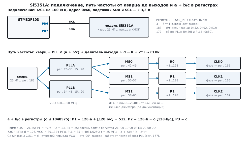
18ж.1 Structure: crystal, two PLLs, three dividers and the registers
The frequency path in the three-output Si5351A (from the manufacturer's documentation, not verified):
f_VCO = f_XTAL · (a + b/c)
f_out = f_VCO / (d · R)
Here f_XTAL is the crystal, f_VCO the frequency of PLLA or PLLB, 600…900 MHz, a = 15…90; d is the output divider, R = 1, 2, 4 … 128.
A 25 MHz crystal feeds two PLLs. Each multiplies it by a fraction a + b/c, where c is up to 1048575 (20 bits). Each output takes one of the two PLLs and divides it with its own MultiSynth divider: by 4, by 6 or by any fraction from 8 to 2048. After it comes the R divider by a power of two. Three outputs and two PLLs: two outputs can have fully independent frequencies, the third divides the PLL of one of them.
The chip answers on I2C at address 0x60. The registers the driver writes:
| register | contents |
|---|---|
| 0 | status: SYS_INIT (bit 7) — still loading, LOL_B, LOL_A — PLL not locked |
| 3 | bit k = 1 — output CLKk disabled |
| 15 | PLL source: 0 — both from the crystal |
| 16–18 | CLK0–CLK2: PDN (bit 7), MS_INT (6), MS_SRC (5) — PLLB, INV (4), CLK_SRC (3:2) = 11 — own divider, IDRV (1:0) — 2, 4, 6, 8 mA |
| 22, 23 | FBA_INT, FBB_INT (bit 6) — integer PLL divider |
| 26–33, 34–41 | P1, P2, P3 of the PLLA and PLLB dividers |
| 42–49, 50–57, 58–65 | P1, P2, P3 of the MS0–MS2 dividers; the third byte holds R (bits 6:4) and DIVBY4 (3:2) |
| 165–167 | CLK0–CLK2 phase offset, 7 bits |
| 177 | reset of PLLA (bit 5) and PLLB (bit 7) |
| 183 | crystal load capacitance, bits 7:6 |
The driver keeps frequencies in millihertz in uint64_t, as in 18е:
900 MHz is 9·10¹¹ mHz, the product with the crystal and the denominator
still fits in 64 bits, and no floating point is needed.
18ж.2 Connecting to the F103 and start-up
The module sits on I2C1: SCL — PB6, SDA — PB7, both pins are FT (p. 32),
but the module is powered from 3.3 V and the pull-ups go to 3.3 V. The bus
runs at 100 kHz, the CCR and TRISE setup is the same as in section 99г,
as in 17.3: CCR = 180, TRISE = 37. The driver only needs writes and a
read of one status byte — single-byte reception, p. 764.
A write is the number of the first register followed by data: the address inside the chip increments by itself. The start-up order (from the manufacturer's documentation, not verified) is: wait for SYS_INIT = 0, disable and power down the outputs, set the crystal capacitance and the PLL source:
    {
        const uint8_t oe[2] = {SI_OE, 0xFF};                /* 1. все выходы выключить */
        const uint8_t pdn[4] = {SI_CLK_CTRL, SI_CLK_PDN, SI_CLK_PDN, SI_CLK_PDN};   /* 2. и обесточить */
        uint8_t cl[2] = {SI_XTAL_CL, xtal_cl};              /* 3. нагрузочная ёмкость кварца */
        const uint8_t src[2] = {SI_PLL_SRC, 0x00};          /* 4. PLLA и PLLB — от кварца */
        if ((rc = wr(oe, 2)) != SI_OK || (rc = wr(pdn, 4)) != SI_OK || (rc = wr(cl, 2)) != SI_OK)
            return rc;
        return wr(src, 2);
    }
The start-up exchanges in the model — 7 transfers, 2510 µs on the bus:
| transfer | what |
|---|---|
00 → 80, 00 → 80, 00 → 00 |
status: SYS_INIT stays set for the first three reads (model assumption), 1 ms pause between them |
03 FF |
all outputs disabled |
10 80 80 80 |
CLK0–CLK2 powered down |
B7 D2 |
crystal capacitance 10 pF |
0F 00 |
both PLLs from the crystal |
No answer at 0x60 — the driver returns SI_E_BUS, −2; SYS_INIT never
clears — SI_E_TIMEOUT, −3, after 100 reads. The first frequency, 10 MHz
on CLK0, takes another 6 transfers, 3000 µs:
1A 00 01 00 10 00 00 00 00 — the PLLA divider, 16 40 — FBA_INT,
2A 00 01 00 2B 00 00 00 00 — the MS0 divider, 10 4F — CLK0 from PLLA,
integer, 8 mA, B1 20 — PLLA reset, 03 FE — CLK0 enabled.
Load capacitance. Register 183: bits 7:6 are 01, 10 or 11 for 6, 8 or
10 pF, the lower six bits are 010010 (from the manufacturer's
documentation, not verified): 0x52, 0x92, 0xD2. Choose the
capacitance for the module's crystal, as in 174.3: the wrong capacitance
shifts the frequency. By how much, the model does not compute; either
way, calibration removes the offset (18ж.6).
18ж.3 a + b/c → P1, P2, P3
A divider is not written as a, b and c. It is written as three numbers (from the manufacturer's documentation, not verified):
P1 = 128·a + floor(128·b/c) − 512
P2 = 128·b − c·floor(128·b/c)
P3 = c
P1 is 18 bits, P2 and P3 are 20 each. Back: a + b/c = (P1 + 512 + P2/P3) / 128. The integer part of 128·b/c goes into P1, the remainder into P2: P1 carries the divider to 1/128, and P2/P3 carries what is finer. For an integer divider b = 0, c = 1: P2 = 0, P3 = 1.
void si_params(si_frac_t f, si_p_t *p)
{
    uint32_t fl = (uint32_t)((128ull * f.b) / f.c);         /* floor(128·b / c) */
    p->p1 = 128u * f.a + fl - 512u;
    p->p2 = 128u * f.b - f.c * fl;
    p->p3 = f.c;
}
Example: 35 + 21/25 (PLL at 896 MHz). 128 · 21 / 25 = 107.52, rounded down — 107; P1 = 4480 + 107 − 512 = 4075; P2 = 2688 − 25 · 107 = 13; P3 = 25. The eight bytes go like this: P3 high byte first, the third byte holds the top two bits of P1 (plus R and DIVBY4 for an output divider), then P1, the sixth byte holds the top four bits of P3 and of P2, then P2:
void si_pack(const si_p_t *p, uint32_t r, int divby4, uint8_t out[8])
{
    out[0] = (uint8_t)(p->p3 >> 8);
    out[1] = (uint8_t)p->p3;
    out[2] = (uint8_t)((r & 7u) << 4 | (divby4 ? SI_DIVBY4 : 0u) | ((p->p1 >> 16) & 3u));
    out[3] = (uint8_t)(p->p1 >> 8);
    out[4] = (uint8_t)p->p1;
    out[5] = (uint8_t)(((p->p3 >> 12) & 0xF0u) | ((p->p2 >> 16) & 0x0Fu));
    out[6] = (uint8_t)(p->p2 >> 8);
    out[7] = (uint8_t)p->p2;
}
The model reassembled a + b/c from the bytes:
| a + b/c | P1 | P2 | P3 | bytes |
|---|---|---|---|---|
| 36 + 0/1 | 4096 | 0 | 1 | 00 01 00 10 00 00 00 00 |
| 35 + 21/25 | 4075 | 13 | 25 | 00 19 00 0F EB 00 00 0D |
| 35 + 621/625 | 4095 | 113 | 625 | 02 71 00 0F FF 00 00 71 |
| 28 + 1/1048575 | 3072 | 128 | 1048575 | FF FF 00 0C 00 F0 00 80 |
| 89 + 1048574/1048575 | 11007 | 1048447 | 1048575 | FF FF 00 2A FF FF FF 7F |
| 8 | 512 | 0 | 1 | 00 01 00 02 00 00 00 00 |
| 126 | 15616 | 0 | 1 | 00 01 00 3D 00 00 00 00 |
| 4 | 0 | 0 | 1 | 00 01 00 00 00 00 00 00 |
Division by 4 is a special case: P1 = P2 = 0, P3 = 1 and DIVBY4 = 11. The formula gives the same P1, P2, P3, but without DIVBY4 the chip does not divide by 4 (from the manufacturer's documentation, not verified).
18ж.4 Dividers: R, an even output divider, a fractional PLL and the frequency error
For one output on its own PLL the driver computes:
- below 500 kHz — enable R: double the frequency until it is at least 500 kHz (R up to 128);
- above 150 MHz — divider 4; otherwise an even integer divider that brings the VCO as close to 900 MHz as possible from below;
- give the fractional part to the PLL: a + b/c = VCO / 25 MHz.
An even integer output divider means MS_INT = 1, and according to the manufacturer's documentation that gives less jitter (not verified: the model does not compute jitter). Only the PLL stays fractional.
int si_plan(const si_t *s, uint64_t f_mhz, si_plan_t *pl)
{
    uint64_t fo;
    if (f_mhz < SI_F_MIN || f_mhz > SI_F_MAX)
        return SI_E_RANGE;
    pl->r = 0;
    while ((f_mhz << pl->r) < SI_R_FLOOR && pl->r < 7u)     /* ниже 500 кГц — поднять частоту делителем R */
        pl->r++;
    fo = f_mhz << pl->r;
    if (fo > 150000000000ull)
        pl->d = 4;                                          /* выше 150 МГц — только деление на 4 */
    else
        pl->d = (uint32_t)(SI_VCO_MAX / fo) & ~1u;          /* чётный, VCO как можно ближе к 900 МГц */
    if (pl->d > SI_MS_MAX)
        pl->d = SI_MS_MAX;
    pl->vco_mhz = fo * pl->d;
    if (pl->vco_mhz < SI_VCO_MIN || pl->vco_mhz > SI_VCO_MAX)
        return SI_E_RANGE;
    pl->pll = si_ratio(pl->vco_mhz, s->xtal_mhz, s->method);
    if (!pll_ok(pl->pll))
        return SI_E_RANGE;
    pl->f_mhz = si_out_mhz(s->xtal_mhz, pl->pll, pl->d, pl->r);
    return SI_OK;
}
Why an even divider always fits: if the frequency is not above 150 MHz, 900 / f is at least 6, and VCO = d · f loses at most two f from 900 MHz — it never drops below 600 MHz.
How to find b/c. The simple way is c = 1048575 always and b the
nearest integer. The other is the best fraction with c ≤ 1048575: the
convergents of the continued fraction and the last semiconvergent, with
no float. The model with a crystal of exactly 25 MHz:
| wanted | R | d | VCO | PLL (best fraction) | error with c = 1048575 |
|---|---|---|---|---|---|
| 8 kHz | 64 | 1756 | 899.072 MHz | 35 + 3009/3125 | +0.022 mHz |
| 10 kHz | 64 | 1406 | 899.84 MHz | 35 + 621/625 | −0.032 mHz |
| 32 768 Hz | 16 | 1716 | 899.678208 MHz | 35 + 385597/390625 | −0.068 mHz |
| 100 kHz | 8 | 1124 | 899.2 MHz | 35 + 121/125 | +1.061 mHz |
| 455 kHz | 2 | 988 | 899.08 MHz | 35 + 602/625 | −5.309 mHz |
| 1 MHz | 1 | 900 | 900 MHz | 36 | 0 |
| 3.579545 MHz | 1 | 250 | 894.88625 MHz | 35 + 15909/20000 | +1.550 mHz |
| 7.074 MHz | 1 | 126 | 891.324 MHz | 35 + 4081/6250 | +88.556 mHz |
| 10 MHz | 1 | 90 | 900 MHz | 36 | 0 |
| 14.074 MHz | 1 | 62 | 872.588 MHz | 34 + 5647/6250 | −186.120 mHz |
| 27 MHz | 1 | 32 | 864 MHz | 34 + 14/25 | 0 |
| 28.8 MHz | 1 | 30 | 864 MHz | 34 + 14/25 | 0 |
| 100 MHz | 1 | 8 | 800 MHz | 32 | 0 |
| 125 MHz | 1 | 6 | 750 MHz | 30 | 0 |
| 148.5 MHz | 1 | 6 | 891 MHz | 35 + 16/25 | 0 |
| 150 MHz | 1 | 6 | 900 MHz | 36 | 0 |
| 160 MHz | 1 | 4 | 640 MHz | 25 + 3/5 | 0 |
With the best fraction all 17 frequencies came out exact — the model
assembled them from the written registers. Below 8 kHz and above 160 MHz
the driver refuses: 7999.999 Hz and 160 000 000.001 Hz both give
SI_E_RANGE, −1.
The error from c ≤ 1048575. With c = 1048575 the PLL step is 25 MHz / 1048575 = 23.8419 Hz at the VCO, divided by d at the output: 0.1892 Hz at 7.074 MHz (d = 126), 0.2649 Hz at 10 MHz, 0.3845 Hz at 14.074 MHz. The error is up to half a step. The model ran 2000 random frequencies from 1 to 100 MHz in 1 Hz steps:
| method | worst error | in ppb | exact |
|---|---|---|---|
| c = 1048575 | 1475.073 mHz | 16.024 | — |
| best fraction | 0.954 mHz | 0.081 | 627 of 2000 |
The worst with c = 1048575 was at 92 055 717 Hz, where d = 8: half a step at the output is 23.8419 / 2 / 8 = 1.4901 Hz. Both errors are smaller than the offset of any crystal: the output frequency is set by the crystal, not by the fraction (18ж.6).
18ж.5 Three outputs on two PLLs, retuning and PLL reset
Two outputs get their own PLL. For the third the driver uses a fractional
divider from an already occupied PLL — si_set_freq_shared. The model:
CLK0 = 7.074 MHz on PLLA, CLK1 = 12.288 MHz on PLLB, CLK2 = 32 768 Hz from
the same PLLB:
| output | PLL | VCO | divider | R | frequency |
|---|---|---|---|---|---|
| CLK0 | A | 891.324 MHz | 126, integer | 1 | 7 074 000.000 Hz |
| CLK1 | B | 884.736 MHz | 72, integer | 1 | 12 288 000.000 Hz |
| CLK2 | B | 884.736 MHz | 1687.5, fractional | 16 | 32 768.000 Hz |
There are 2 PLL resets, one per owner. The fractional CLK2 divider does
not reset the PLL: another output lives on it. If the PLL has no owner
yet, si_set_freq_shared returns SI_E_ARG, −4.
Retuning. A local oscillator over 7.000…7.200 MHz in 1 kHz steps —
201 steps. Within one output divider only the PLL changes, and a step is
one transfer of 9 bytes 1A …, 920 µs at 100 kHz. The divider changed
twice: 128 → 126 at 7032 kHz and 126 → 124 at 7143 kHz. On a change the
output divider, CLK0_CTRL and a PLL reset are added:
    if ((rc = write_pll(s, pll, pl.pll)) != SI_OK)          /* перестройка внутри одного делителя — только PLL */
        return rc;
    s->vco_mhz[pll] = pl.vco_mhz;
    if (changed) {
        si_frac_t ms = {pl.d, 0, 1};
        if ((rc = write_ms(clk, ms, pl.r, pl.d == 4u)) != SI_OK || (rc = write_ctrl(s, clk, ctrl)) != SI_OK)
            return rc;
        s->d[clk] = pl.d;
        s->r[clk] = pl.r;
    }
    if ((changed || s->always_reset) && (rc = si_pll_reset(s, pll)) != SI_OK)   /* новый делитель — сброс PLL */
        return rc;
| PLL reset | resets | transfers | on the bus |
|---|---|---|---|
| only when the divider changes | 2 | 207 | 187 920 µs |
| on every step | 201 | 406 | 245 630 µs |
On all 201 steps the frequency is exactly the one asked for, in both
modes. A reset (register 177: 0x20 — PLLA, 0x80 — PLLB) restarts all
outputs of that PLL at zero phase. In the model the output phase jumped
at every reset — by up to 180.00°; how long the output stays silent
while the PLL relocks, the model does not know (lock is instant in it).
In a receiver this is a click. Reset when the output divider has changed
or when a common phase is needed (18ж.6) — retuning one PLL without a
divider change needs no reset in the model.
18ж.6 Phase offset, I/Q quadrature and calibration against a reference
Phase offset. Registers 165–167 set the output delay in quarters of the VCO period, 7 bits (from the manufacturer's documentation, not verified). With an integer divider d the output period is d VCO periods, and a quarter of the output period is d quarters. Hence quadrature: CLK0 and CLK1 from one PLL with the same integer divider d, CLK0 offset 0, CLK1 offset d. Seven bits mean d no larger than 127, even — 126, and the VCO not below 600 MHz: quadrature only from 600 MHz / 126 = 4.762 MHz.
    ph[0] = SI_PHOFF0;
    ph[1] = 0;
    ph[2] = (uint8_t)pl.d;                                  /* CLK1 позже на d · T_VCO / 4 = четверть периода */
    if ((rc = wr(ctrl, 3)) != SI_OK || (rc = wr(ph, 3)) != SI_OK)
        return rc;
The offset takes effect after a PLL reset (so in the model; from the
manufacturer's documentation, not verified), so si_quadrature always
ends with a PLLA reset. The model:
| frequency | d | VCO | CLK1 lags by | offset step |
|---|---|---|---|---|
| 7.074 MHz | 126 | 891.324 MHz | 90.00° | 0.714° |
| 4.8 MHz | 126 | 604.8 MHz | 90.00° | 0.714° |
| 4.762 MHz | 126 | 600.012 MHz | 90.00° | 0.714° |
| 4.761 MHz | — | — | refused, −1 | — |
| 30 MHz | 30 | 900 MHz | 90.00° | 3° |
| 100 MHz | 8 | 800 MHz | 90.00° | 11.25° |
| 150 MHz | 6 | 900 MHz | 90.00° | 15° |
A quarter of the VCO period at 891.324 MHz is 0.2805 ns. After 12.3 ms the offset is the same, 90.00°. What breaks the quadrature in the model:
- a write to the output divider — the same MS1 bytes once more: the output restarted with another phase, 243.32°; a PLLA reset brought back 90.00°;
- a fractional divider — from PLLA at 900 MHz, 7.074 MHz needs a divider of 127.226463; the offset is an integer, 127, which is 89.84°;
- inversion — the INV bit on CLK1 adds 180°: 270.00°.
Retuning I/Q always involves a reset: si_quadrature to a neighbouring
frequency is 7 transfers, one of them a reset. Two AD9833 chips needed a
common RESET for the same quadrature (18е.2); here one chip and one PLL
are enough.
Calibration. The output accuracy is set by the crystal, not by the fraction. In the model the module's crystal is 25 000 437 Hz, +17.48 ppm (model assumption). The driver computes with 25 MHz, and the very first frequency of 10 MHz came out as 10 000 174.8 Hz. Before calibration: +175 Hz at 10 MHz, +124 Hz at 7.074 MHz, +1748 Hz at 100 MHz. A reference frequency counter (in the model, a 1 s count rounded to 1 Hz) showed 10 000 175 Hz; the driver computes the offset in parts per billion and corrects the crystal frequency:
void si_calibrate(si_t *s, uint64_t f_set_mhz, uint64_t f_meas_mhz)
{
    int64_t e = (int64_t)f_meas_mhz - (int64_t)f_set_mhz;
    int64_t ppb = div_round(e * 1000000000, (int64_t)f_set_mhz);   /* уход кварца в миллиардных долях */
    s->xtal_mhz = (uint64_t)((int64_t)s->xtal_mhz + div_round((int64_t)s->xtal_mhz * ppb, 1000000000));
    s->ppb += (int32_t)ppb;
}
The correction is 17 500 ppb, the crystal for the driver is 25 000 437.5 Hz. After recomputing the dividers: −0.2 Hz at 10 MHz, −0.1415 Hz at 7.074 MHz, −2.0 Hz at 100 MHz. The remainder of 20 ppb is the counter's resolution, 1 Hz at 10 MHz, not the driver's. The higher the comparison frequency and the longer the count, the more accurate the correction. A crystal ages and drifts with temperature (174.4), so calibration is not forever.
18ж.7 Pitfalls
Divider bytes one at a time. A "one register — one transfer" driver
writes the eight divider bytes in eight transfers. In the model written
data takes effect at the end of a transfer (model assumption), and the
change 7.000 → 7.030 MHz went through seven intermediate frequencies of
290 µs each: 6 999 243.482 Hz, three times 6 999 238.281 Hz, three times
7 029 755.859 Hz — and only then 7 030 000.000 Hz. Here the misses are
small, but for another pair of frequencies they can leave the VCO range.
Write the eight bytes in one transfer, as write_pll does; when the real
chip picks up new P1–P3 is not verified.
PLL reset on every step. Many examples reset the PLL after any frequency change. That is 201 resets instead of 2 over 201 retuning steps, 31 % more bus time, and a phase jump at every one (18ж.5). Reset only when the output divider changes or for a common phase.
A low frequency without R. 100 kHz from a 900 MHz VCO needs a divider of 9000, more than 2048. A naive driver writes it anyway: P1 = 1151488, and only 262143 fits in 18 bits. The top bits were lost, the model read a divider of 808 and output 1 113 861.386 Hz instead of 100 kHz. Below 500 kHz use the R divider (18ж.4).
The wrong crystal. Some modules have a 27 MHz crystal. A driver that
computes with 25 MHz produced 10 800 000 Hz in the model for 10 MHz — 8 %
too high. Calibration against a reference corrected the crystal by
80 000 000 ppb, to 27 000 000 Hz, and 10 MHz came out exact. Better read
the crystal marking and pass the right frequency to si_init from the
start.
Quadrature below 4.762 MHz. The offset is 7 bits, the divider for 90° is at most 126 with the VCO no lower than 600 MHz: the driver rejects 4.761 MHz. Below that, I/Q is made differently on HF — for example, an output at 4f and a flip-flop divider; this was not checked here.
Output load and level. The output is CMOS swinging from ground to the output supply, usually 3.3 V on modules, with 2, 4, 6 or 8 mA drive set by the IDRV bits (from the manufacturer's documentation, not verified). It is a square wave, not a sine: an ideal square wave has its 3rd harmonic at −9.54 dB from the fundamental, the 5th at −13.98 dB, the 7th at −16.90 dB; a mixer or a 50 Ω input without a filter gets those too. What a square wave looks like at the end of a cable and why matching matters — 36к.3 and 36к.5. The model does not compute voltages and currents.
Range. 8 kHz…160 MHz is from the manufacturer's documentation (not verified). The dividers would allow more: 2.289 kHz at the bottom (600 MHz / 2048 / 128), but the driver does not promise it and refuses outside 8 kHz…160 MHz.
The output did not turn on. After si_init all outputs are disabled
by register 3 and powered down by the PDN bit. If you write dividers
without the driver, do not forget CLKk_CTRL (clear PDN, CLK_SRC = 11)
and the bit in register 3.
18ж.8 Summary
- Si5351A: address 0x60, 25 MHz crystal → PLLA/PLLB × (a + b/c), 600…900 MHz → output divider 4, 6, 8…2048 → R 1…128 → CLK0–CLK2.
- Start-up: SYS_INIT = 0,
03 FF,10 80 80 80,B7 D2,0F 00— 7 transfers, 2510 µs. - P1 = 128·a + floor(128·b/c) − 512, P2 = 128·b − c·floor(128·b/c), P3 = c: 35 + 21/25 → 4075, 13, 25.
- Below 500 kHz — R; the output divider is an even integer, the PLL is fractional; 7.074 MHz: d = 126, VCO 891.324 MHz, 35 + 4081/6250.
- c = 1048575: a 23.8419 Hz step at the VCO, error up to 1.475 Hz (16 ppb); the best fraction — up to 0.954 mHz.
- Retuning 7.0…7.2 MHz: 2 PLL resets instead of 201, 920 µs per step.
- I/Q: CLK1 offset = d, PLL reset — 90.00°; from 4.762 MHz; a fractional divider — 89.84°.
- Calibration: +17.48 ppm → a 17 500 ppb correction, −0.2 Hz left at 10 MHz.
Full sources
si18h.h — Si5351A bits and registers, structures, driver and platform interface.
/* si18h.h — раздел 18ж: драйвер генератора тактовых частот Si5351A (3 выхода) без регистров STM32.
 * Драйвер считает делители и пишет регистры через функцию платформы si_port_xfer(): запись байтов, затем
 * (если nrx > 0) повторный старт и чтение. В прошивке fw18h.c её даёт I2C1 STM32F103, в стенде host18h.c —
 * модель model18h.py. Адреса регистров и биты — по документации производителя (AN619; в проекте её нет,
 * не проверено), сверены только с моделью. Частоты — в миллигерцах (мГц), чтобы считать без float. */
#ifndef SI18H_H
#define SI18H_H
#include <stdint.h>

#define SI_ADDR         0x60u           /* 7-битный адрес Si5351A */

/* ── регистры ─────────────────────────────────────────────────────────── */
#define SI_STATUS       0u              /* SYS_INIT, LOL_B, LOL_A, LOS, REVID */
#define SI_OE           3u              /* бит k = 1 — выход CLKk выключен */
#define SI_PLL_SRC      15u             /* 0 — обе PLL от кварца */
#define SI_CLK_CTRL     16u             /* 16, 17, 18 — CLK0…CLK2 */
#define SI_FB_CTRL      22u             /* 22 — бит FBA_INT, 23 — FBB_INT */
#define SI_MSNA         26u             /* 26…33 — P1, P2, P3 делителя PLLA */
#define SI_MSNB         34u             /* 34…41 — то же для PLLB */
#define SI_MS0          42u             /* 42 + 8·k — делитель MultiSynth выхода k, R и DIVBY4 */
#define SI_PHOFF0       165u            /* 165 + k — сдвиг фазы CLKk, 7 бит */
#define SI_PLL_RST      177u            /* сброс PLL */
#define SI_XTAL_CL      183u            /* нагрузочная ёмкость кварца */

/* ── биты ─────────────────────────────────────────────────────────────── */
#define SI_SYS_INIT     0x80u           /* статус: микросхема ещё загружается */
#define SI_LOL_B        0x40u
#define SI_LOL_A        0x20u
#define SI_CLK_PDN      0x80u           /* CLKk_CTRL: выход обесточен */
#define SI_CLK_INT      0x40u           /* MSk_INT: делитель выхода целый */
#define SI_CLK_PLLB     0x20u           /* MSk_SRC: от PLLB, иначе от PLLA */
#define SI_CLK_INV      0x10u           /* выход инвертирован: +180° */
#define SI_CLK_SRC_MS   0x0Cu           /* CLKk_SRC = 11: выход от своего MultiSynth */
#define SI_FB_INT       0x40u           /* FBx_INT: делитель PLL целый */
#define SI_DIVBY4       0x0Cu           /* MSk_DIVBY4 = 11: деление на 4 */
#define SI_PLLA_RST     0x20u
#define SI_PLLB_RST     0x80u
#define SI_CL_6PF       0x52u           /* биты 7:6 — 01, 10, 11; биты 5:0 — 010010 */
#define SI_CL_8PF       0x92u
#define SI_CL_10PF      0xD2u

/* ── пределы (по документации производителя, не проверено) ────────────── */
#define SI_C_MAX        1048575u        /* знаменатель c — 20 бит */
#define SI_VCO_MIN      600000000000ull /* 600 МГц в мГц */
#define SI_VCO_MAX      900000000000ull /* 900 МГц */
#define SI_PLL_A_MIN    15u
#define SI_PLL_A_MAX    90u
#define SI_MS_MAX       2048u
#define SI_F_MIN        8000000ull      /* 8 кГц в мГц */
#define SI_F_MAX        160000000000ull /* 160 МГц */
#define SI_R_FLOOR      500000000ull    /* ниже 500 кГц — делитель R */
#define SI_IQ_D_MAX     126u            /* сдвиг фазы — 7 бит: чётный делитель не больше 126 */

enum { SI_OK = 0, SI_E_RANGE = -1, SI_E_BUS = -2, SI_E_TIMEOUT = -3, SI_E_ARG = -4 };
enum { SI_FIXED_C = 0, SI_BEST = 1 };   /* как искать b/c: c = 1048575 или лучшая дробь */

typedef struct { uint32_t a, b, c; } si_frac_t;          /* a + b/c */
typedef struct { uint32_t p1, p2, p3; } si_p_t;          /* то, что ложится в регистры */

typedef struct {
    uint32_t r;                         /* R = 2^r, r = 0…7 */
    uint32_t d;                         /* делитель MultiSynth: 4, 6 или чётный 8…2048 */
    uint64_t vco_mhz;                   /* заказанная частота PLL */
    si_frac_t pll;                      /* делитель PLL: vco / кварц */
    uint64_t f_mhz;                     /* что получится при заданном кварце */
} si_plan_t;

typedef struct {
    uint64_t xtal_mhz;                  /* частота кварца в мГц, с поправкой калибровки */
    int32_t ppb;                        /* поправка калибровки, миллиардные доли */
    uint8_t method;                     /* SI_FIXED_C или SI_BEST */
    uint8_t always_reset;               /* 1 — сбрасывать PLL при каждой смене частоты (как во многих примерах) */
    uint8_t idrv;                       /* сила выхода 0…3: 2, 4, 6, 8 мА */
    uint8_t oe;                         /* копия регистра 3 */
    uint8_t ctrl[3];                    /* копии CLK0…CLK2_CTRL */
    uint8_t fb[2];                      /* копии регистров 22 и 23: FBA_INT, FBB_INT */
    uint32_t d[3], r[3];                /* последние делители выходов: сменились — нужен сброс PLL */
    uint64_t vco_mhz[2];                /* что сейчас на PLLA и PLLB */
    uint32_t resets;                    /* сколько раз сбрасывали PLL */
} si_t;

/* ── платформа: прошивка или стенд ────────────────────────────────────── */
int si_port_xfer(uint8_t addr7, const uint8_t *tx, uint32_t ntx, uint8_t *rx, uint32_t nrx);
void si_port_delay_us(uint32_t us);

/* ── арифметика ───────────────────────────────────────────────────────── */
si_frac_t si_ratio(uint64_t num, uint64_t den, int method);   /* num/den ≈ a + b/c, c ≤ 1048575 */
void si_params(si_frac_t f, si_p_t *p);                       /* a + b/c -> P1, P2, P3 */
void si_pack(const si_p_t *p, uint32_t r, int divby4, uint8_t out[8]);
uint64_t si_out_mhz(uint64_t xtal_mhz, si_frac_t pll, uint32_t d, uint32_t r);
int si_plan(const si_t *s, uint64_t f_mhz, si_plan_t *pl);   /* R, чётный делитель, дробная PLL */
int si_plan_iq(const si_t *s, uint64_t f_mhz, si_plan_t *pl);/* для I/Q: делитель не больше 126 */

/* ── управление ───────────────────────────────────────────────────────── */
int si_init(si_t *s, uint32_t xtal_hz, uint8_t xtal_cl);
int si_set_freq(si_t *s, int clk, int pll, uint64_t f_mhz);  /* своя PLL: чётный делитель, дробная PLL */
int si_set_freq_shared(si_t *s, int clk, int pll, uint64_t f_mhz);  /* PLL уже занята: дробный делитель выхода */
int si_quadrature(si_t *s, uint64_t f_mhz);                   /* CLK0 и CLK1 на PLLA, CLK1 отстаёт на 90° */
int si_pll_reset(si_t *s, int pll);
int si_output(si_t *s, int clk, int on);
int si_invert(si_t *s, int clk, int inv);
void si_calibrate(si_t *s, uint64_t f_set_mhz, uint64_t f_meas_mhz);  /* по эталонному частотомеру */

#endif
si18h.c — a + b/c and the best fraction, P1–P3, divider plan, start-up, retuning, I/Q and calibration.
/* si18h.c — раздел 18ж: драйвер Si5351A. Только делители и регистры; шину даёт si_port_xfer() платформы. */
#include "si18h.h"
static int wr(const uint8_t *b, uint32_t n)
{
return si_port_xfer(SI_ADDR, b, n, 0, 0); /* b[0] — номер первого регистра, дальше подряд */
}
static int64_t div_round(int64_t n, int64_t d) /* d > 0 */
{
return n >= 0 ? (n + d / 2) / d : -((-n + d / 2) / d);
}
/* ── арифметика ───────────────────────────────────────────────────────── */
static uint64_t dist(uint64_t p, uint64_t q, uint64_t rem, uint64_t den) /* |p/q − rem/den| · q · den */
{
uint64_t x = p * den, y = rem * q;
return x > y ? x - y : y - x;
}
si_frac_t si_ratio(uint64_t num, uint64_t den, int method)
{
si_frac_t f;
uint64_t rem = num % den, b;
f.a = (uint32_t)(num / den);
f.b = 0;
f.c = 1;
if (rem == 0)
return f;
if (method == SI_FIXED_C) {
b = (rem * SI_C_MAX + den / 2u) / den; /* c = 1048575, b — ближайшее целое */
f.c = SI_C_MAX;
} else { /* лучшая дробь с c ≤ 1048575: цепная дробь */
uint64_t p0 = 0, q0 = 1, p1 = 1, q1 = 0, n = rem, d = den;
while (d) {
uint64_t t = n / d, p2 = t * p1 + p0, q2 = t * q1 + q0, m;
if (q2 > SI_C_MAX) { /* дальше нельзя: проверить промежуточную дробь */
uint64_t k = (SI_C_MAX - q0) / q1, ps = p0 + k * p1, qs = q0 + k * q1;
if (dist(ps, qs, rem, den) * q1 < dist(p1, q1, rem, den) * qs) {
p1 = ps;
q1 = qs;
}
break;
}
p0 = p1;
q0 = q1;
p1 = p2;
q1 = q2;
m = n - t * d;
n = d;
d = m;
}
b = p1;
f.c = (uint32_t)q1;
}
if (b >= f.c) { /* округлилось до целого */
f.a++;
b = 0;
}
if (b == 0)
f.c = 1;
f.b = (uint32_t)b;
return f;
}
void si_params(si_frac_t f, si_p_t *p)
{
uint32_t fl = (uint32_t)((128ull * f.b) / f.c); /* floor(128·b / c) */
p->p1 = 128u * f.a + fl - 512u;
p->p2 = 128u * f.b - f.c * fl;
p->p3 = f.c;
}
void si_pack(const si_p_t *p, uint32_t r, int divby4, uint8_t out[8])
{
out[0] = (uint8_t)(p->p3 >> 8);
out[1] = (uint8_t)p->p3;
out[2] = (uint8_t)((r & 7u) << 4 | (divby4 ? SI_DIVBY4 : 0u) | ((p->p1 >> 16) & 3u));
out[3] = (uint8_t)(p->p1 >> 8);
out[4] = (uint8_t)p->p1;
out[5] = (uint8_t)(((p->p3 >> 12) & 0xF0u) | ((p->p2 >> 16) & 0x0Fu));
out[6] = (uint8_t)(p->p2 >> 8);
out[7] = (uint8_t)p->p2;
}
uint64_t si_out_mhz(uint64_t xtal_mhz, si_frac_t pll, uint32_t d, uint32_t r)
{
uint64_t num = xtal_mhz * ((uint64_t)pll.a * pll.c + pll.b); /* VCO · c */
uint64_t den = ((uint64_t)pll.c * d) << r;
return (num + den / 2u) / den;
}
static int pll_ok(si_frac_t f)
{
return f.a >= SI_PLL_A_MIN && (f.a < SI_PLL_A_MAX || (f.a == SI_PLL_A_MAX && f.b == 0));
}
int si_plan(const si_t *s, uint64_t f_mhz, si_plan_t *pl)
{
uint64_t fo;
if (f_mhz < SI_F_MIN || f_mhz > SI_F_MAX)
return SI_E_RANGE;
pl->r = 0;
while ((f_mhz << pl->r) < SI_R_FLOOR && pl->r < 7u) /* ниже 500 кГц — поднять частоту делителем R */
pl->r++;
fo = f_mhz << pl->r;
if (fo > 150000000000ull)
pl->d = 4; /* выше 150 МГц — только деление на 4 */
else
pl->d = (uint32_t)(SI_VCO_MAX / fo) & ~1u; /* чётный, VCO как можно ближе к 900 МГц */
if (pl->d > SI_MS_MAX)
pl->d = SI_MS_MAX;
pl->vco_mhz = fo * pl->d;
if (pl->vco_mhz < SI_VCO_MIN || pl->vco_mhz > SI_VCO_MAX)
return SI_E_RANGE;
pl->pll = si_ratio(pl->vco_mhz, s->xtal_mhz, s->method);
if (!pll_ok(pl->pll))
return SI_E_RANGE;
pl->f_mhz = si_out_mhz(s->xtal_mhz, pl->pll, pl->d, pl->r);
return SI_OK;
}
int si_plan_iq(const si_t *s, uint64_t f_mhz, si_plan_t *pl)
{
uint64_t d;
if (f_mhz < SI_F_MIN || f_mhz > SI_F_MAX)
return SI_E_RANGE;
d = (SI_VCO_MAX / f_mhz) & ~1ull;
if (d > SI_IQ_D_MAX)
d = SI_IQ_D_MAX; /* сдвиг на 90° = d четвертей периода VCO, 7 бит */
if (d < 6u)
return SI_E_RANGE;
pl->r = 0;
pl->d = (uint32_t)d;
pl->vco_mhz = f_mhz * d;
if (pl->vco_mhz < SI_VCO_MIN)
return SI_E_RANGE; /* ниже 600 МГц / 126 = 4,762 МГц I/Q нет */
pl->pll = si_ratio(pl->vco_mhz, s->xtal_mhz, s->method);
if (!pll_ok(pl->pll))
return SI_E_RANGE;
pl->f_mhz = si_out_mhz(s->xtal_mhz, pl->pll, pl->d, 0);
return SI_OK;
}
/* ── регистры ─────────────────────────────────────────────────────────── */
int si_init(si_t *s, uint32_t xtal_hz, uint8_t xtal_cl)
{
uint8_t reg = SI_STATUS, st = SI_SYS_INIT;
int rc;
for (uint32_t i = 0; st & SI_SYS_INIT; i++) { /* пока SYS_INIT = 1, микросхема не готова */
if (i == 100u)
return SI_E_TIMEOUT;
if ((rc = si_port_xfer(SI_ADDR, ®, 1, &st, 1)) != SI_OK)
return rc; /* нет ответа на 0x60: провод, питание, адрес */
if (st & SI_SYS_INIT)
si_port_delay_us(1000u);
}
s->xtal_mhz = (uint64_t)xtal_hz * 1000u;
s->ppb = 0;
s->method = SI_BEST;
s->always_reset = 0;
s->idrv = 3; /* 8 мА */
s->oe = 0xFF;
s->resets = 0;
for (int k = 0; k < 3; k++) {
s->ctrl[k] = SI_CLK_PDN;
s->d[k] = s->r[k] = 0;
}
s->fb[0] = s->fb[1] = 0xFF; /* ещё не писали */
s->vco_mhz[0] = s->vco_mhz[1] = 0;
{
const uint8_t oe[2] = {SI_OE, 0xFF}; /* 1. все выходы выключить */
const uint8_t pdn[4] = {SI_CLK_CTRL, SI_CLK_PDN, SI_CLK_PDN, SI_CLK_PDN}; /* 2. и обесточить */
uint8_t cl[2] = {SI_XTAL_CL, xtal_cl}; /* 3. нагрузочная ёмкость кварца */
const uint8_t src[2] = {SI_PLL_SRC, 0x00}; /* 4. PLLA и PLLB — от кварца */
if ((rc = wr(oe, 2)) != SI_OK || (rc = wr(pdn, 4)) != SI_OK || (rc = wr(cl, 2)) != SI_OK)
return rc;
return wr(src, 2);
}
}
static int write_pll(si_t *s, int pll, si_frac_t f)
{
si_p_t p;
uint8_t b[9];
uint8_t fb = f.b ? 0u : SI_FB_INT; /* целый делитель PLL — FBx_INT = 1 */
int rc;
si_params(f, &p);
b[0] = (uint8_t)(pll ? SI_MSNB : SI_MSNA);
si_pack(&p, 0, 0, b + 1);
if ((rc = wr(b, 9)) != SI_OK) /* все 8 байт — одной посылкой */
return rc;
if (s->fb[pll] != fb) {
uint8_t w[2] = {(uint8_t)(SI_FB_CTRL + pll), fb};
if ((rc = wr(w, 2)) != SI_OK)
return rc;
s->fb[pll] = fb;
}
return SI_OK;
}
static int write_ms(int clk, si_frac_t f, uint32_t r, int divby4)
{
si_p_t p;
uint8_t b[9];
if (divby4) {
p.p1 = p.p2 = 0; /* деление на 4: P1 = P2 = 0, P3 = 1 */
p.p3 = 1;
} else {
si_params(f, &p);
}
b[0] = (uint8_t)(SI_MS0 + 8u * (uint32_t)clk);
si_pack(&p, r, divby4, b + 1);
return wr(b, 9);
}
static int write_ctrl(si_t *s, int clk, uint8_t v)
{
uint8_t w[2] = {(uint8_t)(SI_CLK_CTRL + clk), v};
s->ctrl[clk] = v;
return wr(w, 2);
}
int si_pll_reset(si_t *s, int pll)
{
uint8_t w[2] = {SI_PLL_RST, pll ? SI_PLLB_RST : SI_PLLA_RST};
s->resets++;
return wr(w, 2);
}
int si_output(si_t *s, int clk, int on)
{
uint8_t w[2];
if (clk < 0 || clk > 2)
return SI_E_ARG;
s->oe = (uint8_t)(on ? s->oe & ~(1u << clk) : s->oe | (1u << clk));
w[0] = SI_OE;
w[1] = s->oe;
return wr(w, 2);
}
int si_invert(si_t *s, int clk, int inv)
{
if (clk < 0 || clk > 2)
return SI_E_ARG;
return write_ctrl(s, clk, (uint8_t)(inv ? s->ctrl[clk] | SI_CLK_INV : s->ctrl[clk] & ~SI_CLK_INV));
}
int si_set_freq(si_t *s, int clk, int pll, uint64_t f_mhz)
{
si_plan_t pl;
int rc, changed;
uint8_t ctrl;
if (clk < 0 || clk > 2 || pll < 0 || pll > 1)
return SI_E_ARG;
if ((rc = si_plan(s, f_mhz, &pl)) != SI_OK)
return rc;
ctrl = (uint8_t)(SI_CLK_INT | (pll ? SI_CLK_PLLB : 0u) | SI_CLK_SRC_MS | s->idrv | (s->ctrl[clk] & SI_CLK_INV));
changed = s->d[clk] != pl.d || s->r[clk] != pl.r || (s->ctrl[clk] & ~SI_CLK_INV) != (ctrl & ~SI_CLK_INV);
if ((rc = write_pll(s, pll, pl.pll)) != SI_OK) /* перестройка внутри одного делителя — только PLL */
return rc;
s->vco_mhz[pll] = pl.vco_mhz;
if (changed) {
si_frac_t ms = {pl.d, 0, 1};
if ((rc = write_ms(clk, ms, pl.r, pl.d == 4u)) != SI_OK || (rc = write_ctrl(s, clk, ctrl)) != SI_OK)
return rc;
s->d[clk] = pl.d;
s->r[clk] = pl.r;
}
if ((changed || s->always_reset) && (rc = si_pll_reset(s, pll)) != SI_OK) /* новый делитель — сброс PLL */
return rc;
return (s->oe & (1u << clk)) ? si_output(s, clk, 1) : SI_OK;
}
int si_set_freq_shared(si_t *s, int clk, int pll, uint64_t f_mhz)
{
uint64_t fo, vco = s->vco_mhz[pll < 0 || pll > 1 ? 0 : pll];
uint32_t r = 0;
si_frac_t ms;
uint8_t ctrl;
int rc;
if (clk < 0 || clk > 2 || pll < 0 || pll > 1 || vco == 0)
return SI_E_ARG; /* сначала частоту получает хозяин PLL */
if (f_mhz < SI_F_MIN || f_mhz > SI_F_MAX)
return SI_E_RANGE;
while ((f_mhz << r) < SI_R_FLOOR && r < 7u)
r++;
fo = f_mhz << r;
ms = si_ratio(vco, fo, s->method); /* делитель выхода дробный: a + b/c */
if (ms.a < 8u || ms.a > SI_MS_MAX || (ms.a == SI_MS_MAX && ms.b))
return SI_E_RANGE;
ctrl = (uint8_t)((ms.b ? 0u : SI_CLK_INT) | (pll ? SI_CLK_PLLB : 0u) | SI_CLK_SRC_MS | s->idrv | (s->ctrl[clk] & SI_CLK_INV));
if ((rc = write_ms(clk, ms, r, 0)) != SI_OK || (rc = write_ctrl(s, clk, ctrl)) != SI_OK)
return rc;
s->d[clk] = 0; /* не чётный делитель: следующий si_set_freq сбросит PLL */
s->r[clk] = r;
return (s->oe & (1u << clk)) ? si_output(s, clk, 1) : SI_OK; /* PLL не сбрасываем: на ней чужой выход */
}
int si_quadrature(si_t *s, uint64_t f_mhz)
{
si_plan_t pl;
si_frac_t ms;
uint8_t ctrl[3], ph[3];
int rc;
if ((rc = si_plan_iq(s, f_mhz, &pl)) != SI_OK)
return rc;
if ((rc = write_pll(s, 0, pl.pll)) != SI_OK)
return rc;
s->vco_mhz[0] = pl.vco_mhz;
ms.a = pl.d;
ms.b = 0;
ms.c = 1;
if ((rc = write_ms(0, ms, 0, 0)) != SI_OK || (rc = write_ms(1, ms, 0, 0)) != SI_OK)
return rc;
ctrl[0] = SI_CLK_CTRL;
ctrl[1] = ctrl[2] = (uint8_t)(SI_CLK_INT | SI_CLK_SRC_MS | s->idrv); /* оба от PLLA, делитель целый */
ph[0] = SI_PHOFF0;
ph[1] = 0;
ph[2] = (uint8_t)pl.d; /* CLK1 позже на d · T_VCO / 4 = четверть периода */
if ((rc = wr(ctrl, 3)) != SI_OK || (rc = wr(ph, 3)) != SI_OK)
return rc;
s->ctrl[0] = s->ctrl[1] = ctrl[1];
for (int k = 0; k < 2; k++) {
s->d[k] = pl.d;
s->r[k] = 0;
}
if ((rc = si_pll_reset(s, 0)) != SI_OK) /* без сброса фазы CLK0 и CLK1 не связаны */
return rc;
s->oe = (uint8_t)(s->oe & ~3u);
{
uint8_t w[2] = {SI_OE, s->oe};
return wr(w, 2);
}
}
void si_calibrate(si_t *s, uint64_t f_set_mhz, uint64_t f_meas_mhz)
{
int64_t e = (int64_t)f_meas_mhz - (int64_t)f_set_mhz;
int64_t ppb = div_round(e * 1000000000, (int64_t)f_set_mhz); /* уход кварца в миллиардных долях */
s->xtal_mhz = (uint64_t)((int64_t)s->xtal_mhz + div_round((int64_t)s->xtal_mhz * ppb, 1000000000));
s->ppb += (int32_t)ppb;
}
fw18h.c — F103 firmware: I2C1 at 100 kHz, quadrature on CLK0/CLK1, 10 MHz on CLK2, calibration via the debugger.
/* fw18h.c — раздел 18ж: генератор на Si5351A, STM32F103 (BluePill), 72 МГц, APB1 = 36 МГц.
 * I2C1: PB6 — SCL, PB7 — SDA (открытый сток, 100 кГц, подтяжки на модуле или 4,7 кОм к 3,3 В). При запуске —
 * ожидание SYS_INIT, выходы выключены, кварц 25 МГц с ёмкостью 10 пФ. Затем: CLK0 и CLK1 — квадратура I/Q на
 * tune_hz (PLLA, CLK1 позже на 90°), CLK2 — 10 МГц от PLLB. Через отладчик: tune_hz — новая частота I/Q;
 * cal_set_hz и cal_meas_hz — что заказали на CLK2 и что показал эталонный частотомер (после записи обоих — поправка
 * в ppb и перестройка). Тактирование до 72 МГц — как в разделе 6. */
#include "stm32f10x.h"
#include "si18h.h"

#define CPU_HZ          72000000u
#define APB1_MHZ        36u
#define I2C_TIMEOUT_US  2000u           /* байт на 100 кГц — 90 мкс */
#define XTAL_HZ         25000000u

static si_t si;
volatile uint32_t tune_hz = 7074000u, cal_set_hz, cal_meas_hz, bus_errors;
volatile int32_t si_rc = 1, cal_ppb;

static int expired(uint32_t t0, uint32_t us)
{
    return DWT->CYCCNT - t0 >= us * (CPU_HZ / 1000000u);
}

void si_port_delay_us(uint32_t us)
{
    uint32_t t0 = DWT->CYCCNT;
    while (!expired(t0, us)) {
    }
}

static void gpio_i2c1_init(void)
{
    RCC->APB2ENR |= RCC_APB2ENR_IOPBEN | RCC_APB2ENR_AFIOEN;
    RCC->APB1ENR |= RCC_APB1ENR_I2C1EN;
    /* PB6, PB7 — альтернативная функция, открытый сток, 2 МГц (1110) */
    GPIOB->CRL = (GPIOB->CRL & 0x00FFFFFFu) | 0xEE000000u;
    I2C1->CR1 = 0;                                      /* настраивать при PE = 0 */
    I2C1->CR2 = APB1_MHZ;
    I2C1->CCR = APB1_MHZ * 1000000u / (2u * 100000u);   /* стандартный режим: 36 МГц / (2 × 180) = 100 кГц */
    I2C1->TRISE = APB1_MHZ + 1u;                        /* 1000 нс × 36 МГц = 36 → 37 */
    I2C1->CR1 = I2C_CR1_PE;
}

static int sr1_wait(uint16_t mask)
{
    uint32_t t0 = DWT->CYCCNT;
    while (!(I2C1->SR1 & mask)) {
        if (I2C1->SR1 & I2C_SR1_AF)
            return SI_E_BUS;                            /* адрес или байт не подтверждён */
        if (expired(t0, I2C_TIMEOUT_US))
            return SI_E_BUS;
    }
    return SI_OK;
}

static int fail(int rc)
{
    I2C1->CR1 |= I2C_CR1_STOP;
    I2C1->SR1 = (uint16_t)~I2C_SR1_AF;                  /* AF снимается записью нуля */
    I2C1->CR1 |= I2C_CR1_ACK;
    bus_errors++;
    return rc;
}

int si_port_xfer(uint8_t addr7, const uint8_t *tx, uint32_t ntx, uint8_t *rx, uint32_t nrx)
{
    int rc;
    uint32_t t0 = DWT->CYCCNT;
    if (nrx > 1u || (nrx != 0u && ntx == 0u))
        return SI_E_ARG;                                /* драйверу хватает одного байта статуса */
    while (I2C1->SR2 & I2C_SR2_BUSY) {                  /* SDA держит ведомый — раздел 17.6 */
        if (expired(t0, I2C_TIMEOUT_US))
            return SI_E_BUS;
    }
    I2C1->CR1 |= I2C_CR1_START;
    if ((rc = sr1_wait(I2C_SR1_SB)) != SI_OK)
        return fail(rc);
    I2C1->DR = (uint8_t)(addr7 << 1);
    if ((rc = sr1_wait(I2C_SR1_ADDR)) != SI_OK)
        return fail(rc);
    (void)I2C1->SR2;
    for (uint32_t i = 0; i < ntx; i++) {                /* номер регистра, затем данные: адрес растёт сам */
        if ((rc = sr1_wait(I2C_SR1_TXE)) != SI_OK)
            return fail(rc);
        I2C1->DR = tx[i];
    }
    if ((rc = sr1_wait(I2C_SR1_BTF)) != SI_OK)
        return fail(rc);
    if (!nrx) {
        I2C1->CR1 |= I2C_CR1_STOP;
        return SI_OK;
    }
    I2C1->CR1 |= I2C_CR1_START;                         /* повторный старт: номер регистра уже передан */
    if ((rc = sr1_wait(I2C_SR1_SB)) != SI_OK)
        return fail(rc);
    I2C1->DR = (uint8_t)(addr7 << 1 | 1u);
    if ((rc = sr1_wait(I2C_SR1_ADDR)) != SI_OK)
        return fail(rc);
    I2C1->CR1 &= (uint16_t)~I2C_CR1_ACK;                /* один байт — RM0008, с. 764: NACK до снятия ADDR */
    (void)I2C1->SR2;
    I2C1->CR1 |= I2C_CR1_STOP;
    if ((rc = sr1_wait(I2C_SR1_RXNE)) != SI_OK)
        return fail(rc);
    rx[0] = (uint8_t)I2C1->DR;
    I2C1->CR1 |= I2C_CR1_ACK;
    return SI_OK;
}

static int start_outputs(uint32_t iq_hz)
{
    int rc;
    if ((rc = si_quadrature(&si, (uint64_t)iq_hz * 1000u)) != SI_OK)
        return rc;                                      /* ниже 4,762 МГц I/Q нет */
    return si_set_freq(&si, 2, 1, 10000000000ull);      /* CLK2 — 10 МГц от PLLB */
}

int main(void)
{
    uint32_t cur = 0;
    CoreDebug->DEMCR |= CoreDebug_DEMCR_TRCENA_Msk;
    DWT->CYCCNT = 0;
    DWT->CTRL |= DWT_CTRL_CYCCNTENA_Msk;
    gpio_i2c1_init();
    while ((si_rc = si_init(&si, XTAL_HZ, SI_CL_10PF)) != SI_OK)
        si_port_delay_us(100000u);                      /* нет ответа на 0x60: провод, питание */
    for (;;) {
        if (cal_set_hz && cal_meas_hz) {                /* эталон: что заказали и что намерили */
            si_calibrate(&si, (uint64_t)cal_set_hz * 1000u, (uint64_t)cal_meas_hz * 1000u);
            cal_ppb = si.ppb;
            cal_set_hz = cal_meas_hz = 0;
            cur = 0;                                    /* пересчитать все делители с новым кварцем */
        }
        if (tune_hz != cur) {
            cur = tune_hz;
            si_rc = start_outputs(cur);
        }
        si_port_delay_us(10000u);
    }
}
Next: section 19 "The CAN bus" — an interface for communication between boards and nodes.