 Embedded HandbookApps
18е. DDS generator AD9833 over SPI: phase accumulator, frequency and phase, sine/triangle/square, sweep and FSK
How a DDS works inside — the phase accumulator, the sine table, the phase truncation spurs and the images around the sample rate — was covered in sections 36к.2 and 36к.4, and a generator on the STM32's own DAC in 15.4 and 36к.8. Here is a ready DDS chip on a small module: the AD9833 with a 25 MHz crystal oscillator. The microcontroller only writes words to it over SPI: frequency, phase, waveform. We look at which words and in what order, how to change the frequency without a phase jump, how to make a sweep and FSK, what the spectrum shows and what to put after the output. SPI is in section 18, its modes in 18.2.
Sources: RM0008 (DocID13902 Rev 17): APB2 up to 72 MHz, APB1 up to 36 MHz,
p. 48; the SPI1EN bit, p. 112; TIM2EN, p. 116; SPI pins — table 25,
p. 166: the master's SCK and MOSI are an alternate function, NSS under
software management is an ordinary pin; without remap SPI1 is on PA4–PA7,
p. 185; the master's hardware NSS is held low while the SPI is enabled,
p. 703; the DFF bit — 16-bit frame, p. 742; BR[2:0], p. 743; CPOL and
CPHA, p. 744; the BSY flag, p. 745; the TXE flag, p. 746. DocID13587
Rev 17 (STM32F103x8/xB): PA4–PA7 are not 5 V tolerant, p. 29. There is no
AD9833 document in the project and no driver on disk either: the word
bits, the start-up order, the SPI mode and the output levels are taken
from the manufacturer's documentation (Analog Devices) and not verified.
All numbers below come from running the driver _verify/dds18g/ad18g.c on
a computer (gcc 12.2.0) with our own AD9833 model in Python 3.11; the
firmware is built with armclang 6.24 for Cortex-M3.
What it is called in the documentation
Original Meaning DDS — direct digital synthesis direct digital synthesis phase accumulator phase accumulator MCLK — master clock the chip's clock frequency FREQREG, PHASEREG frequency word, phase word FSYNC chip select, active low SFDR — spurious-free dynamic range margin to the worst spur dBc decibels relative to the signal itself image a copy of the signal around MCLK sweep frequency sweep FSK / PSK frequency / phase shift keying
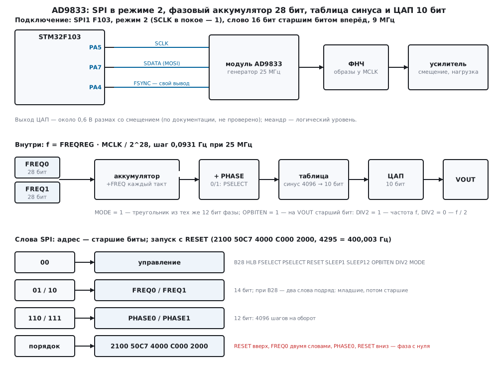
18е.1 The principle: a 28-bit accumulator, a table and a 10-bit DAC
Inside the AD9833 is the same scheme as in 36к.2, only in silicon (according to the manufacturer's documentation, not verified): a 28-bit phase accumulator adds the frequency word FREQREG on every MCLK clock; the top 12 bits of the phase select a point of the sine table; the point goes to a 10-bit DAC. Hence
f = FREQREG · MCLK / 2^28 FREQREG = round(f · 2^28 / MCLK)
At MCLK = 25 MHz the frequency step is 25 000 000 / 2^28 = 0.0931 Hz: this is the "0.1 Hz resolution". The first clocks of the model at 1 MHz — word 10737418, the table point number grows by 163.84 per clock:
| clock | accumulator | table point | DAC code |
|---|---|---|---|
| 0 | 0 | 0 | 512 |
| 1 | 10737418 | 163 | 638 |
| 2 | 21474836 | 327 | 757 |
| 3 | 32212254 | 491 | 861 |
| 4 | 42949672 | 655 | 943 |
| 5 | 53687090 | 819 | 998 |
| 6 | 64424508 | 983 | 1022 |
| 7 | 75161926 | 1146 | 1014 |
That is 25 samples per period: a 1 MHz sine leaves the DAC in steps, and only the filter after the output smooths them (18е.4). The model's table has codes from 0 to 1023, the middle is 512.
The driver computes the frequency word in integers: the frequency in millihertz, a 64-bit division with rounding. So the firmware needs no floating point:
uint32_t ad_freq_word(uint64_t f_mhz, uint32_t mclk_hz)
{
    uint64_t den = (uint64_t)mclk_hz * 1000u;               /* f в мГц: FREQREG = f · 2^28 / MCLK */
    if (f_mhz >= (1ull << 35))
        return AD_FREQ_MAX;                                 /* больше 34 ГГц — сдвиг переполнил бы 64 бита */
    uint64_t w = ((f_mhz << AD_PHASE_BITS) + den / 2u) / den;
    return w > AD_FREQ_MAX ? AD_FREQ_MAX : (uint32_t)w;
}
| requested | FREQREG | obtained |
|---|---|---|
| 0.1 Hz | 1 | 0.093 Hz |
| 1 Hz | 11 | 1.024 Hz |
| 400 Hz | 4295 (0x10C7) |
400.003 Hz |
| 1 kHz | 10737 | 999.961 Hz |
| 1234.56 Hz | 13256 | 1234.561 Hz |
| 100 kHz | 1073742 | 100 000.016 Hz |
| 1 MHz | 10737418 | 999 999.978 Hz |
| 5 MHz | 53687091 | 4 999 999.981 Hz |
| 12.5 MHz | 134217728 (0x8000000) |
12 500 000 Hz |
At low frequencies the step shows: 1 Hz comes out as 1.024 Hz. 12.5 MHz is half of MCLK, the Nyquist limit; in practice above a few megahertz the DAC steps and the images (18е.4) spoil the sine far more than the resolution allows for.
The phase is 12 bits, 4096 steps per turn, a step of 360 / 4096 = 0.088°. The driver computes the word from thousandths of a degree: 0.1° → 1, 1° → 11, 45° → 512, 90° → 1024, 180° → 2048, 270° → 3072, and 359.999° rounds to a full turn — 0.
Registers (according to the manufacturer's documentation, not
verified). The word address is in the top bits: 00 is control, 01 is
FREQ0, 10 is FREQ1, 110 is PHASE0, 111 is PHASE1. The control word
bits the driver uses:
| bit | name | what it does |
|---|---|---|
| 13 | B28 | frequency in two consecutive words: 14 low bits, then 14 high bits |
| 12 | HLB | with B28 = 0: which half the frequency word carries |
| 11 | FSELECT | the output counts by FREQ1 |
| 10 | PSELECT | PHASE1 is added to the phase |
| 8 | RESET | the accumulator is held at zero, the output stands |
| 7 | SLEEP1 | MCLK stopped |
| 6 | SLEEP12 | DAC switched off |
| 5 | OPBITEN | the top bit goes to the output instead of the DAC |
| 3 | DIV2 | with OPBITEN: the top bit as is or divided by 2 |
| 1 | MODE | triangle instead of sine |
18е.2 Connecting to the F103 and starting with RESET
The AD9833 only receives: three wires — SCLK, SDATA and FSYNC, no answer. On the F103 this is SPI1: SCLK on PA5, SDATA is MOSI on PA7, both pins are an alternate function (table 25, p. 166). FSYNC is the ordinary output PA4: the driver frames each transfer with it itself. Hardware NSS will not do: the master keeps it low the whole time the SPI is enabled (p. 703), while the AD9833 tells the start of a word by FSYNC.
A word is 16 bits, most significant bit first, so DFF = 1 (p. 742). The
AD9833 takes a bit on the falling edge of SCLK, and SCLK idles high
(according to the manufacturer's documentation, not verified): that is
mode 2, CPOL = 1, CPHA = 0 (p. 744; modes — 18.2). The rate is
72 MHz / 8 = 9 MHz (BR = 010, p. 743), one word takes 1.778 µs. PA4–PA7
do not tolerate 5 V (p. 29): the module is powered from 3.3 V.
void ad_spi16(const uint16_t *w, uint32_t n)
{
    FSYNC_LO();
    for (uint32_t i = 0; i < n; i++) {
        while (!(SPI1->SR & SPI_SR_TXE)) {
        }
        SPI1->DR = w[i];                        /* слова идут подряд: FSYNC внизу всю посылку */
    }
    while (!(SPI1->SR & SPI_SR_TXE)) {
    }
    while (SPI1->SR & SPI_SR_BSY) {             /* TXE мало: последнее слово ещё выдвигается */
    }
    FSYNC_HI();
}
Several words in a row under one FSYNC are fine: the AD9833 counts bits in
16s (according to the manufacturer's documentation, not verified). FSYNC
goes up only after BSY clears (p. 745), as in 18.4: TXE rises while the
last word is still in the shift register (18е.7).
Start-up. After power-on the register contents are undefined, and the
generator immediately outputs something. In the model the first chip
came up with the control word 1CE2: square wave, MCLK stopped, DAC off.
The start-up order (according to the manufacturer's documentation, not
verified) is RESET up, the frequency and phase words, RESET down:
void ad_init(ad_t *a, uint32_t mclk_hz, uint32_t freq_word, uint16_t phase_word, int wave)
{
    a->mclk_hz = mclk_hz;
    a->ctrl = (uint16_t)(AD_CTRL | AD_B28 | wave_bits(wave));
    uint16_t w[5] = {
        (uint16_t)(AD_CTRL | AD_B28 | AD_RESET),             /* 2100: RESET держит выход, пока пишем */
        (uint16_t)(AD_FREQ0 | LO14(freq_word)),             /* FREQ0, младшие 14 бит */
        (uint16_t)(AD_FREQ0 | HI14(freq_word)),             /* FREQ0, старшие 14 бит */
        (uint16_t)(AD_PHASE0 | (phase_word & 0x0FFFu)),
        a->ctrl,                                            /* RESET = 0: пуск с нулевой фазы */
    };
    ad_spi16(w, 5);
}
For 400 Hz these are the words 2100 50C7 4000 C000 2000: the word
4295 = 0x10C7 fits entirely into the low 14 bits, the high ones are
zeros. The model received them as 5 words of 1.778 µs; the frequency
became 400.003 Hz after the third word. While RESET is set, the output
holds the table code for PHASE0: before PHASE0 was written there was a
random value — code 111, after it the middle of the scale, 512. After
RESET was released the sine started from 512, codes from 0 to 1023, and
counting periods by crossings of the middle gave 400.00 Hz.
RESET is needed not only against garbage: it zeroes the accumulator, and the phase starts from a known place. Two chips from one 25 MHz oscillator, frequency 999 450.68 Hz:
| how they were started | shift of B relative to A |
|---|---|
| the same words, without RESET | 293.71° — whatever it was after power-on |
ad_init to both in one transfer |
0.00° |
| RESET, PHASE0 = 1024 on B, RESET released by one word to both | 90.00° |
| the same, but RESET released in turn, in two transfers | 176.75° |
The shift was computed separately from the output codes of both chips (one DFT harmonic over 16 384 samples). In the last row B started 44 MCLK clocks later — one SPI word, 1.76 µs — and that is 633.25° at this frequency. An I/Q generator (sine and cosine) works only if RESET is released by one word with both FSYNC lines low.
18е.3 Frequency and phase: two half-words, B28 and a change without a break
The frequency word is 28 bits, and an SPI word holds 14. With B28 = 1 they
are written in two consecutive words, low bits first, and the register
changes only after the second (according to the manufacturer's
documentation, not verified) — that is what ad_set_freq does. With
B28 = 0 the HLB bit selects the half, and it changes at once.
Model: frequency 999 000.017 Hz, change to 1 001 000.032 Hz.
| method | words | intermediate frequency | how long it lasted |
|---|---|---|---|
| in halves (B28 = 0, HLB) | 5 | 997 948.274 Hz | 3555.6 ns — two words |
ad_set_freq (B28 = 1) |
2 | none | — |
The new low 14 bits with the old high ones give a third frequency nobody asked for. For a sweep with a fine step this is a glitch; if the low half crosses the 14-bit boundary, the miss can be large too. Writing in halves pays only when the high half does not change: then it is one word.
Without a phase break. A new frequency word changes only the rate at which the accumulator grows — the phase itself continues from where it was. Many examples online change the frequency through RESET: RESET up, the word, RESET down. The model at 10 kHz compared both paths:
| frequency change | phase jump | output stands |
|---|---|---|
ad_set_freq 10 → 12 kHz |
none | no |
| RESET, word, start, 12 → 10 kHz | 83.98° — to zero | 135 clocks, 5.4 µs |
With RESET the output jumped by 509 codes in one clock — a click in audio and a break on the oscilloscope. RESET is needed only at start-up and to synchronise several chips.
The phase changes the same way — a word 110 or 111 with 12 bits.
PHASE is added to the top bits of the accumulator, so writing PHASE is an
instant phase jump by the difference of the words.
18е.4 Sine, triangle, square and the spectrum
The waveform is selected by three bits (according to the manufacturer's documentation, not verified): MODE = 1 is a triangle from the same 12 phase bits, OPBITEN = 1 sends the top bit to the output instead of the DAC, DIV2 passes it as is or divided by 2. Model at 10 kHz, 1 ms:
| waveform | bits | output | frequency | share of ones |
|---|---|---|---|---|
| sine | — | codes 0…1023, 1024 levels | 10 000 Hz | — |
| triangle | MODE | codes 0…1023, 1024 levels | 10 000 Hz | — |
| square | OPBITEN, DIV2 | 0 and 1 | 10 000 Hz | 0.5 |
| square / 2 | OPBITEN | 0 and 1 | 5000 Hz | 0.5 |
The square wave is a logic level, not the DAC output: its swing is the module supply, not 0.6 V (according to the manufacturer's documentation, not verified).
The sine spectrum. For the spectrum to land exactly on bins, the frequency word is a multiple of 2^12 and the record is 65 536 samples at 25 MHz: then the signal makes exactly m periods (the same trick as in 36к.2). The spurs were computed three times: the model's real path (12 phase bits, 10-bit DAC), phase truncation only with an exact sine, and the 10-bit DAC only with the full phase:
| m | frequency | worst spur | 12-bit phase only | 10-bit DAC only |
|---|---|---|---|---|
| 1 | 381.470 Hz | −72.19 dBc | −72.19 dBc | −83.18 dBc |
| 101 | 38 528.442 Hz | −72.19 dBc | −72.19 dBc | −83.18 dBc |
| 2621 | 999 832.153 Hz | −72.19 dBc | −72.19 dBc | −83.18 dBc |
| 2624 | 1 000 976.562 Hz | −76.64 dBc | none | −76.64 dBc |
| 13107 | 4 999 923.706 Hz | −72.19 dBc | −72.19 dBc | −83.18 dBc |
The worst spur is set by the phase truncation to 12 bits, not by the DAC: −72.19 dBc against −72.24 dBc by the −6.02 dB per bit estimate from 36к.2. At m = 2624 the word is a multiple of 2^16, the dropped bits are always zeros, there is no truncation — only the DAC remains, −76.64 dBc. For m = 7, 1001 and 6553 — the same −72.19 dBc.
Images. The DAC holds every sample until the next one, and copies of the signal appear around MCLK at 25 MHz − f and 25 MHz + f (36к.4). Model: the samples stretched into steps 8 times, and the spectrum:
| f | at MCLK − f | at MCLK + f | by the sinc formula | droop at f |
|---|---|---|---|---|
| 1 000 976.6 Hz | −27.39 dBc | −28.05 dBc | −27.60 and −28.29 dBc | −0.023 dB |
| 4 998 779.3 Hz | −11.91 dBc | −15.25 dBc | −12.04 and −15.56 dBc | −0.579 dB |
At 5 MHz the image at 20 MHz is only 12 dB weaker than the signal — without a filter this is not a sine. A Butterworth filter with a 6 MHz cutoff (how to build one — section 178):
| order | attenuation at 20 MHz | resulting image | loss at 5 MHz |
|---|---|---|---|
| 3 | 31.38 dB | −42.03 dBc | 1.253 dB |
| 4 | 41.83 dB | −52.84 dBc | 0.907 dB |
| 5 | 52.29 dB | −63.55 dBc | 0.649 dB |
| 6 | 62.75 dB | −74.20 dBc | 0.460 dB |
| 7 | 73.21 dB | −84.79 dBc | 0.325 dB |
For the image to go below the truncation spurs up to 5 MHz, a sixth-order filter is needed. If 1 MHz is enough, the image at 24 MHz is already 27 dB lower, and the same order gives a much larger margin. How to look at the spectrum with the oscilloscope FFT and where it lies — section 36л.10.
18е.5 Sweep by timer and FSK/PSK
Sweep. A timer changes the frequency: TIM2 (TIM2EN, p. 116) raises an
interrupt once every 1 ms, the handler takes the next word and writes it
with ad_set_freq — two SPI words, 32 bits, 3.556 µs on the bus:
void TIM2_IRQHandler(void)
{
    TIM2->SR = (uint16_t)~TIM_SR_UIF;
    if (!ad_sweep_next(&sw)) {
        sweep_start();
        (void)ad_sweep_next(&sw);
    }
    ad_set_freq(&gen, 0, sw.word);              /* без RESET: фаза продолжается */
}
A linear sweep 1 → 10 kHz in 900 steps: the word step is 107.374, not an
integer. The driver computes every word from the start,
w0 + (w1 − w0) · k / steps, rather than adding a step: the model went
from 999.961 to 9999.983 Hz, the deviation from the straight line is no
more than 0.0852 Hz, less than one step of 0.0931 Hz. Adding the integer
step 107, the sweep would have ended at 9968.597 Hz.
A logarithmic sweep 100 Hz → 100 kHz in 300 steps, 100 steps per decade:
each word is r = 10^0.01 = 1.0232929923 times the previous one. The driver
keeps the word in Q16 and multiplies by r without floating point:
acc += acc · mul / 2^32, where mul = (r − 1) · 2^32 = 100042640.
static uint64_t mul_q32(uint64_t a, uint32_t m)             /* a · m / 2^32 без переполнения 64 бит */
{
    return (a >> 32) * m + (((a & 0xFFFFFFFFu) * m) >> 32);
}
Model: from 100.024 to 100 024.0445 Hz, the deviation from 100.024 · r^k is no more than 0.0722 Hz. The start is shifted: 100 Hz is the word 1074, and the 0.0931 Hz step at 100 Hz is already 931 parts per million. Not a single RESET in both sweeps — the phase is continuous. A sweep with an oscilloscope and an RC circuit — 36н.3.
FSK. The two frequencies sit in FREQ0 and FREQ1, a bit switches
FSELECT — one control word, 1.778 µs. Model: 1200 Hz is "1", 2200 Hz is
"0", 1200 baud, 8 bits 10110010. The accumulator is not touched on
switching: not a single phase jump, neighbouring samples (1 µs apart)
differ by no more than 8 codes.
PSK. PHASE0 = 0, PHASE1 = 2048, a bit switches PSELECT. The same 8 bits gave 5 jumps of exactly 180.0° — one per bit change — and neighbouring samples differed by up to 747 codes. The spectrum of the modulation on an FFT — 36н.11.
Switching by an SPI word is tied to the interrupt time: the bit changes 1.778 µs after the transfer starts, and the timer jitter and the interrupt entry delay land on the bit boundary.
18е.6 Output stage and sleep
The AD9833 DAC output is about 0.6 V peak to peak, and not from zero but with an offset (according to the manufacturer's documentation, not verified). For a bench generator one puts after the module:
- a low-pass filter — against the images around 25 MHz (18е.4);
- a coupling capacitor or offset subtraction — so the sine swings around zero;
- an op-amp amplifier — up to the needed swing; the op-amp bandwidth must cover the top frequency with margin;
- a buffer to the load — the chip output itself expects a high-impedance input; a 50 Ω cable and matching — 36к.3.
The model does not compute voltages: the figures for swing, offset and load current here are from the documentation only and not verified.
Sleep. SLEEP1 stops MCLK: the accumulator stands, the output freezes at the last code. SLEEP12 switches the DAC off (according to the manufacturer's documentation, not verified). Model at 10 kHz: SLEEP1 for 20 µs — the output stands at code 1001 for 549 clocks; after waking the sine lagged by 72.00° — exactly 20 µs at 10 kHz. SLEEP12 for 10 µs — 295 clocks without output. If the phase relative to another chip matters, after sleep they are started together again through RESET (18е.2).
18е.7 Pitfalls
Wrong SPI mode. In modes 0 and 3 the data changes on the same SCLK falling edge on which the AD9833 takes it — which bit it sees is decided by nanoseconds. The model in that case takes one of the two neighbouring bits at random: of 405 words of start-up and 200 frequency changes, 22 arrived correct in mode 0 and 23 in mode 3; the frequency instead of 8362.9973 Hz was 12 183 296.77 Hz and 7093.05 Hz. In modes 1 and 2 — all 405. The documentation draws SCLK idling high, hence mode 2.
FSYNC on every byte. A driver "for 8 bits" raises FSYNC after every byte — the word breaks at the 8th bit and is discarded. In the model none of the 5 start-up words arrived: 10 fragments, the registers stayed random. With an 8-bit frame but FSYNC over the whole word — all 5 accepted.
FSYNC on TXE instead of BSY. TXE rises when the last word has
only just gone into the shift register. In the model FSYNC went up after
the first bit of the last word: 4 words of 5 accepted, the last — the
RESET release — discarded. The generator is silent: the output stands at
512.
No RESET at start-up. The output right after power-on is anything: frequency, waveform, sleep are random (18е.2). And without RESET two chips cannot be synchronised: 293.71° instead of 0°.
Resolution is not accuracy. 0.0931 Hz is the word step, while accuracy
is set by the 25 MHz oscillator on the module. The model with a crystal at
+30 ppm, 25 000 750 Hz: 1 MHz requested — 1 000 029.98 Hz obtained, an
error of 322 steps. The cure is calibration: measure the frequency,
compute the real MCLK and pass it to ad_freq_word — the same formula gave
999 999.99 Hz. The oscillator tolerance on a particular module is not
verified.
Changing the frequency through RESET. A phase jump and an output
standing for 5.4 µs (18е.3). For sweeps and FSK — only ad_set_freq and
FSELECT.
18е.8 Summary
- f = FREQREG · 25 MHz / 2^28: step 0.0931 Hz; 400 Hz is the word 4295, 400.003 Hz; 1 MHz is 10737418.
- The phase is 12 bits: 90° is 1024, step 0.088°.
- SPI1 of the F103: mode 2, 16-bit frame, 9 MHz — 1.778 µs per word; FSYNC
is our own pin, raised after
BSY. - Start-up:
2100 50C7 4000 C000 2000; RESET gives a known phase: two chips — 0.00° and 90.00° for I/Q. - B28: two words, no intermediate frequency; in halves — 997 948.274 Hz for 3555.6 ns.
- A frequency change without RESET has no phase jump; through RESET — 83.98° and 5.4 µs of silence.
- The worst sine spur is −72.19 dBc from phase truncation; the 10-bit DAC gives −83.18 dBc.
- The image at 5 MHz is −11.91 dBc; a 6th-order Butterworth at 6 MHz gives −74.20 dBc.
- Sweep 1 → 10 kHz in 900 steps — error up to 0.0852 Hz; 100 Hz → 100 kHz in 300 steps — up to 0.0722 Hz.
- FSK 1200/2200 Hz without phase jumps; PSK — 180.0°.
Full sources
ad18g.h — AD9833 word bits, structures and the driver and platform interface.
/* ad18g.h — раздел 18е: драйвер DDS-генератора AD9833 без регистров STM32.
 * Драйвер собирает 16-битные слова и отдаёт их функции платформы ad_spi16(): FSYNC вниз, слова, FSYNC вверх.
 * В прошивке fw18g.c её даёт STM32F103 (SPI1, режим 2), в стенде host18g.c — модель model18g.py.
 * Биты слов AD9833 — по документации производителя (в проекте её нет, не проверено). */
#ifndef AD18G_H
#define AD18G_H
#include <stdint.h>

/* ── адрес слова: два старших бита (у фазы — три) ────────────────────── */
#define AD_CTRL       0x0000u           /* 00 — регистр управления */
#define AD_FREQ0      0x4000u           /* 01 — FREQ0, 14 бит данных */
#define AD_FREQ1      0x8000u           /* 10 — FREQ1 */
#define AD_PHASE0     0xC000u           /* 110 — PHASE0, 12 бит данных */
#define AD_PHASE1     0xE000u           /* 111 — PHASE1 */

/* ── биты регистра управления ─────────────────────────────────────────── */
#define AD_B28        (1u << 13)        /* частота — двумя словами подряд: 14 младших, потом 14 старших бит */
#define AD_HLB        (1u << 12)        /* при B28 = 0: 1 — слово несёт старшие 14 бит, 0 — младшие */
#define AD_FSELECT    (1u << 11)        /* выход считает по FREQ1 */
#define AD_PSELECT    (1u << 10)        /* к фазе прибавляется PHASE1 */
#define AD_RESET      (1u << 8)         /* аккумулятор фазы в ноль, выход — середина шкалы */
#define AD_SLEEP1     (1u << 7)         /* MCLK остановлен: аккумулятор стоит */
#define AD_SLEEP12    (1u << 6)         /* ЦАП выключен */
#define AD_OPBITEN    (1u << 5)         /* на выход — старший бит, а не ЦАП: меандр */
#define AD_DIV2       (1u << 3)         /* при OPBITEN: 1 — старший бит как есть, 0 — он же, делённый на 2 */
#define AD_MODE       (1u << 1)         /* треугольник вместо синуса (только при OPBITEN = 0) */

#define AD_PHASE_BITS 28u               /* разрядность аккумулятора */
#define AD_FREQ_MAX   ((1ul << 28) - 1u)

enum { AD_SINE, AD_TRIANGLE, AD_SQUARE, AD_SQUARE_DIV2 };

typedef struct {
    uint32_t mclk_hz;                   /* частота кварцевого генератора модуля: 25 000 000 */
    uint16_t ctrl;                      /* последнее слово управления (без RESET) */
} ad_t;

typedef struct {
    uint32_t w0, w1, steps, k;          /* начало, конец, число шагов, номер шага */
    uint64_t acc;                       /* логарифмический: слово частоты в Q16 */
    uint32_t mul;                       /* логарифмический: (r - 1) · 2^32, r — отношение соседних шагов */
    uint32_t word;                      /* текущее слово частоты */
    uint8_t log;
} ad_sweep_t;

/* ── платформа: прошивка или стенд ────────────────────────────────────── */
void ad_spi16(const uint16_t *w, uint32_t n);   /* FSYNC вниз, n слов старшим битом вперёд, FSYNC вверх */

/* ── расчёт слов ──────────────────────────────────────────────────────── */
uint32_t ad_freq_word(uint64_t f_mhz, uint32_t mclk_hz);     /* f в мГц -> FREQREG, с округлением */
uint64_t ad_freq_mhz(uint32_t word, uint32_t mclk_hz);       /* FREQREG -> f в мГц, с округлением */
uint16_t ad_phase_word(uint32_t mdeg);                       /* фаза в тысячных градуса -> PHASEREG */

/* ── управление ───────────────────────────────────────────────────────── */
void ad_init(ad_t *a, uint32_t mclk_hz, uint32_t freq_word, uint16_t phase_word, int wave);
void ad_set_freq(ad_t *a, int reg, uint32_t word);           /* B28: два слова за одну посылку */
void ad_set_freq_half(ad_t *a, int reg, uint32_t word);      /* B28 = 0: младшие и старшие 14 бит отдельно */
void ad_set_phase(ad_t *a, int reg, uint16_t word);
void ad_wave(ad_t *a, int wave);
void ad_select(ad_t *a, int fsel, int psel);                 /* FSK и PSK: одно слово управления */
void ad_sleep(ad_t *a, uint16_t bits);                       /* AD_SLEEP1, AD_SLEEP12 или 0 */
void ad_reset_hold(ad_t *a);                                 /* RESET = 1: выход держит середину шкалы */
void ad_run(ad_t *a);                                        /* RESET = 0: пуск с нулевой фазы */

/* ── свип частоты: шаг — по таймеру ───────────────────────────────────── */
void ad_sweep_lin(ad_sweep_t *s, uint32_t w0, uint32_t w1, uint32_t steps);
void ad_sweep_log(ad_sweep_t *s, uint32_t w0, uint32_t mul, uint32_t steps);
int ad_sweep_next(ad_sweep_t *s);       /* 1 — новое слово в s->word, 0 — свип закончен */

#endif
ad18g.c — frequency and phase words, start-up with RESET, B28, FSK/PSK, sleep and sweep.
/* ad18g.c — раздел 18е: драйвер AD9833. Только слова и арифметика; шину даёт ad_spi16() платформы. */
#include "ad18g.h"

#define LO14(w) ((uint16_t)((w) & 0x3FFFu))
#define HI14(w) ((uint16_t)(((w) >> 14) & 0x3FFFu))

uint32_t ad_freq_word(uint64_t f_mhz, uint32_t mclk_hz)
{
    uint64_t den = (uint64_t)mclk_hz * 1000u;               /* f в мГц: FREQREG = f · 2^28 / MCLK */
    if (f_mhz >= (1ull << 35))
        return AD_FREQ_MAX;                                 /* больше 34 ГГц — сдвиг переполнил бы 64 бита */
    uint64_t w = ((f_mhz << AD_PHASE_BITS) + den / 2u) / den;
    return w > AD_FREQ_MAX ? AD_FREQ_MAX : (uint32_t)w;
}

uint64_t ad_freq_mhz(uint32_t word, uint32_t mclk_hz)
{
    return ((uint64_t)word * mclk_hz * 1000u + (1u << (AD_PHASE_BITS - 1u))) >> AD_PHASE_BITS;
}

uint16_t ad_phase_word(uint32_t mdeg)
{
    return (uint16_t)((((uint64_t)mdeg * 4096u + 180000u) / 360000u) & 0x0FFFu);   /* 4096 шагов на оборот */
}

static uint16_t wave_bits(int wave)
{
    switch (wave) {
    case AD_TRIANGLE:    return AD_MODE;
    case AD_SQUARE:      return AD_OPBITEN | AD_DIV2;            /* старший бит: частота f */
    case AD_SQUARE_DIV2: return AD_OPBITEN;                      /* старший бит, делённый на 2: f / 2 */
    default:             return 0;
    }
}

void ad_init(ad_t *a, uint32_t mclk_hz, uint32_t freq_word, uint16_t phase_word, int wave)
{
    a->mclk_hz = mclk_hz;
    a->ctrl = (uint16_t)(AD_CTRL | AD_B28 | wave_bits(wave));
    uint16_t w[5] = {
        (uint16_t)(AD_CTRL | AD_B28 | AD_RESET),             /* 2100: RESET держит выход, пока пишем */
        (uint16_t)(AD_FREQ0 | LO14(freq_word)),             /* FREQ0, младшие 14 бит */
        (uint16_t)(AD_FREQ0 | HI14(freq_word)),             /* FREQ0, старшие 14 бит */
        (uint16_t)(AD_PHASE0 | (phase_word & 0x0FFFu)),
        a->ctrl,                                            /* RESET = 0: пуск с нулевой фазы */
    };
    ad_spi16(w, 5);
}

void ad_set_freq(ad_t *a, int reg, uint32_t word)
{
    uint16_t base = reg ? AD_FREQ1 : AD_FREQ0;
    uint16_t w[2] = {(uint16_t)(base | LO14(word)), (uint16_t)(base | HI14(word))};
    (void)a;                            /* B28 уже стоит в слове управления */
    ad_spi16(w, 2);
}

void ad_set_freq_half(ad_t *a, int reg, uint32_t word)
{
    uint16_t base = reg ? AD_FREQ1 : AD_FREQ0;
    uint16_t c = (uint16_t)(a->ctrl & ~AD_B28);
    uint16_t w[5] = {
        c,                                                  /* B28 = 0, HLB = 0: следующее слово — младшие 14 бит */
        (uint16_t)(base | LO14(word)),
        (uint16_t)(c | AD_HLB),                             /* HLB = 1: старшие 14 бит */
        (uint16_t)(base | HI14(word)),
        a->ctrl,                                            /* обратно B28 */
    };
    ad_spi16(w, 5);
}

void ad_set_phase(ad_t *a, int reg, uint16_t word)
{
    uint16_t w = (uint16_t)((reg ? AD_PHASE1 : AD_PHASE0) | (word & 0x0FFFu));
    (void)a;
    ad_spi16(&w, 1);
}

void ad_wave(ad_t *a, int wave)
{
    a->ctrl = (uint16_t)((a->ctrl & ~(AD_MODE | AD_OPBITEN | AD_DIV2)) | wave_bits(wave));
    ad_spi16(&a->ctrl, 1);
}

void ad_select(ad_t *a, int fsel, int psel)
{
    a->ctrl = (uint16_t)((a->ctrl & ~(AD_FSELECT | AD_PSELECT)) | (fsel ? AD_FSELECT : 0u) | (psel ? AD_PSELECT : 0u));
    ad_spi16(&a->ctrl, 1);
}

void ad_sleep(ad_t *a, uint16_t bits)
{
    a->ctrl = (uint16_t)((a->ctrl & ~(AD_SLEEP1 | AD_SLEEP12)) | (bits & (AD_SLEEP1 | AD_SLEEP12)));
    ad_spi16(&a->ctrl, 1);
}

void ad_reset_hold(ad_t *a)
{
    uint16_t w = (uint16_t)(a->ctrl | AD_RESET);
    ad_spi16(&w, 1);
}

void ad_run(ad_t *a)
{
    ad_spi16(&a->ctrl, 1);
}

/* ── свип ─────────────────────────────────────────────────────────────── */
void ad_sweep_lin(ad_sweep_t *s, uint32_t w0, uint32_t w1, uint32_t steps)
{
    s->w0 = w0;
    s->w1 = w1;
    s->steps = steps;
    s->k = 0;
    s->log = 0;
    s->word = w0;
}

void ad_sweep_log(ad_sweep_t *s, uint32_t w0, uint32_t mul, uint32_t steps)
{
    s->w0 = w0;
    s->steps = steps;
    s->k = 0;
    s->log = 1;
    s->mul = mul;
    s->acc = (uint64_t)w0 << 16;
    s->word = w0;
}

static uint64_t mul_q32(uint64_t a, uint32_t m)             /* a · m / 2^32 без переполнения 64 бит */
{
    return (a >> 32) * m + (((a & 0xFFFFFFFFu) * m) >> 32);
}

int ad_sweep_next(ad_sweep_t *s)
{
    if (s->k > s->steps)
        return 0;
    if (s->log) {
        if (s->k)
            s->acc += mul_q32(s->acc, s->mul);             /* шаг: умножить на r */
        s->word = (uint32_t)((s->acc + 0x8000u) >> 16);
    } else {                                               /* считать от начала: ошибка не копится */
        int64_t d = (int64_t)s->w1 - (int64_t)s->w0;
        int64_t num = d * (int64_t)s->k;
        int64_t half = (int64_t)(s->steps / 2u);
        s->word = (uint32_t)((int64_t)s->w0 + (num >= 0 ? (num + half) : (num - half)) / (int64_t)s->steps);
    }
    if (s->word > AD_FREQ_MAX)
        s->word = AD_FREQ_MAX;
    s->k++;
    return 1;
}
fw18g.c — F103 firmware: SPI1 in mode 2, FSYNC on PA4, sweep on TIM2.
/* fw18g.c — раздел 18е: DDS-генератор AD9833 на STM32F103 (BluePill), 72 МГц.
 *   SPI1 без ремапа: PA5 — SCLK, PA7 — SDATA (MOSI); PA4 — FSYNC, обычный выход (ведём сами); MISO не нужен.
 *   Режим 2 (CPOL = 1, CPHA = 0): SCLK в покое — единица, AD9833 берёт бит по спаду. Кадр 16 бит (DFF),
 *   72 МГц / 8 = 9 МГц. Кварцевый генератор модуля — 25 МГц.
 *   TIM2 — шаг свипа раз в 1 мс: логарифмический 100 Гц → 100 кГц за 300 шагов (FW_SWEEP = 1)
 *   или линейный 1 → 10 кГц за 900 шагов (FW_SWEEP = 0); в конце свип начинается заново.
 * Тактирование до 72 МГц — как в разделе 6 (здесь не повторяется); APB2 = 72 МГц, APB1 = 36 МГц,
 * таймеры APB1 — 72 МГц. */
#include "stm32f10x.h"
#include "ad18g.h"

#ifndef FW_SWEEP
#define FW_SWEEP 1
#endif
#define MCLK_HZ  25000000u
#define TIM_HZ   72000000u
#define SPI_BR   SPI_CR1_BR_1                   /* BR = 010: fPCLK / 8 */
#define LOG_MUL  100042640u                     /* (10^0,01 - 1) · 2^32: 100 шагов на декаду */

_Static_assert(SPI_BR == 0x10u, "BR[2:0] = 010 — биты 5:3 SPI_CR1");
_Static_assert(SPI_CR1_CPOL == 0x2u && SPI_CR1_CPHA == 0x1u, "CPOL — бит 1, CPHA — бит 0");
_Static_assert(SPI_CR1_DFF == 0x800u, "DFF — бит 11: кадр 16 бит");
_Static_assert(TIM_HZ / 72u / 1000u == 1000u, "TIM2: 72 МГц / 72 / 1000 = 1 кГц");

#define FSYNC_LO() (GPIOA->BRR = 1u << 4)
#define FSYNC_HI() (GPIOA->BSRR = 1u << 4)

void ad_spi16(const uint16_t *w, uint32_t n)
{
    FSYNC_LO();
    for (uint32_t i = 0; i < n; i++) {
        while (!(SPI1->SR & SPI_SR_TXE)) {
        }
        SPI1->DR = w[i];                        /* слова идут подряд: FSYNC внизу всю посылку */
    }
    while (!(SPI1->SR & SPI_SR_TXE)) {
    }
    while (SPI1->SR & SPI_SR_BSY) {             /* TXE мало: последнее слово ещё выдвигается */
    }
    FSYNC_HI();
}

static ad_t gen;
static ad_sweep_t sw;

static void sweep_start(void)
{
#if FW_SWEEP
    ad_sweep_log(&sw, ad_freq_word(100000u, MCLK_HZ), LOG_MUL, 300);
#else
    ad_sweep_lin(&sw, ad_freq_word(1000000u, MCLK_HZ), ad_freq_word(10000000u, MCLK_HZ), 900);
#endif
}

void TIM2_IRQHandler(void)
{
    TIM2->SR = (uint16_t)~TIM_SR_UIF;
    if (!ad_sweep_next(&sw)) {
        sweep_start();
        (void)ad_sweep_next(&sw);
    }
    ad_set_freq(&gen, 0, sw.word);              /* без RESET: фаза продолжается */
}

static void board_init(void)
{
    RCC->APB2ENR |= RCC_APB2ENR_IOPAEN | RCC_APB2ENR_SPI1EN;
    RCC->APB1ENR |= RCC_APB1ENR_TIM2EN;
    FSYNC_HI();                                 /* FSYNC вверх до настройки вывода */
    GPIOA->CRL = (GPIOA->CRL & 0x0F00FFFFu)
               | 0x3u << 16                     /* PA4 — выход: FSYNC */
               | 0xBu << 20                     /* PA5 — SCLK, альтернативная функция */
               | 0xBu << 28;                    /* PA7 — SDATA */
    SPI1->CR1 = SPI_CR1_MSTR | SPI_CR1_CPOL | SPI_CR1_DFF | SPI_BR | SPI_CR1_SSM | SPI_CR1_SSI;   /* режим 2 */
    SPI1->CR1 |= SPI_CR1_SPE;
    TIM2->PSC = 72u - 1u;                       /* 1 МГц */
    TIM2->ARR = 1000u - 1u;                     /* 1 мс */
    TIM2->DIER = TIM_DIER_UIE;
}

int main(void)
{
    board_init();
    ad_init(&gen, MCLK_HZ, ad_freq_word(1000000u, MCLK_HZ), 0, AD_SINE);   /* 1 кГц, пока свип не пошёл */
    sweep_start();
    NVIC_EnableIRQ(TIM2_IRQn);
    TIM2->CR1 = TIM_CR1_CEN;
    for (;;)
        __WFI();
}
Next: section 19 "The CAN bus" — an interface for communication between boards and nodes.