 Embedded HandbookApps
18д. NFC module PN532: frames over I2C/SPI/UART, ACK, reading the UID and NTAG2xx, emulation and the difference from RC522
Section 18г covered the RC522 reader: there the firmware itself writes the MFRC522 registers, runs the anticollision, computes CRC_A and waits for the card's answer by a timer. The PN532 module works in the same 13.56 MHz band and with the same ISO 14443A cards, but is built differently: inside it is a microcontroller of its own with its own firmware, and talking to it means commands and answers in frames with checksums. Here: the frame, three buses to choose from, finding a tag and its UID, the pages of NTAG213 and NTAG215 tags, writing and reading a link in the NDEF format, sleep, timeouts and what to do when the PN532 is silent. The dual-interface tag ST25DV was in section 94а, I²C in section 17, SPI in section 18.
Sources: RM0008 (DocID13902 Rev 17): APB2 up to 72 MHz, APB1 up to 36 MHz,
p. 48; the SPI1EN bit, p. 112; I2C1EN and USART2EN, p. 115; the USART,
SPI and I²C pins, tables 24, 25 and 27, pp. 165–167; without remap SPI1 is
PA4–PA7, USART2 is TX/PA2, RX/PA3, I2C1 is SCL/PB6, SDA/PB7, p. 185;
SPI_CR1: LSBFIRST (bit 7) and BR[2:0], p. 743; I2C_CR1.ACK, p. 774;
FREQ, p. 776; the AF flag, p. 779; SB and ADDR, p. 781; CCR and
TRISE, p. 784; the USART TXE and RXNE flags, p. 819. DocID13587
Rev 17 (STM32F103x8/xB): PA2–PA7 are not 5 V tolerant, p. 29; PA9 is,
p. 31; PB6 and PB7 are 5 V tolerant, p. 32. The project has no PN532
document, and there is no PN532 driver either in the Zephyr tree or in other
sources on disk: the frame format, command and answer codes, the address,
the SPI bus bytes and the UART wake-up are taken from the manufacturer's
documentation and not checked. The NTAG tag commands, their sizes and the
NDEF layout are checked against the Flipper Zero firmware sources (commit
7f0b6e1). All numbers below come from a run of the driver
_verify/nfc18f/pn18f.c on a computer (gcc 12.2.0) with our own model of
the PN532 and the tags in Python 3.11; the firmware is built by armclang
6.24 for the Cortex-M3.
What it is called in the documentation
Original Meaning host controller the host: our microcontroller normal / extended information frame normal / extended frame LEN, LCS — length checksum the length and its checksum TFI — frame identifier the frame direction: D4 or D5 DCS — data checksum the data checksum ACK / NACK frame the "received" / "repeat" frame error frame error frame HSU — high speed UART the module's UART SAM — security access module an external security module SENS_RES / SEL_RES ATQA / SAK from section 18г target, initiator tag, reader CC — capability container the NDEF service page TLV — type, length, value type, length, value
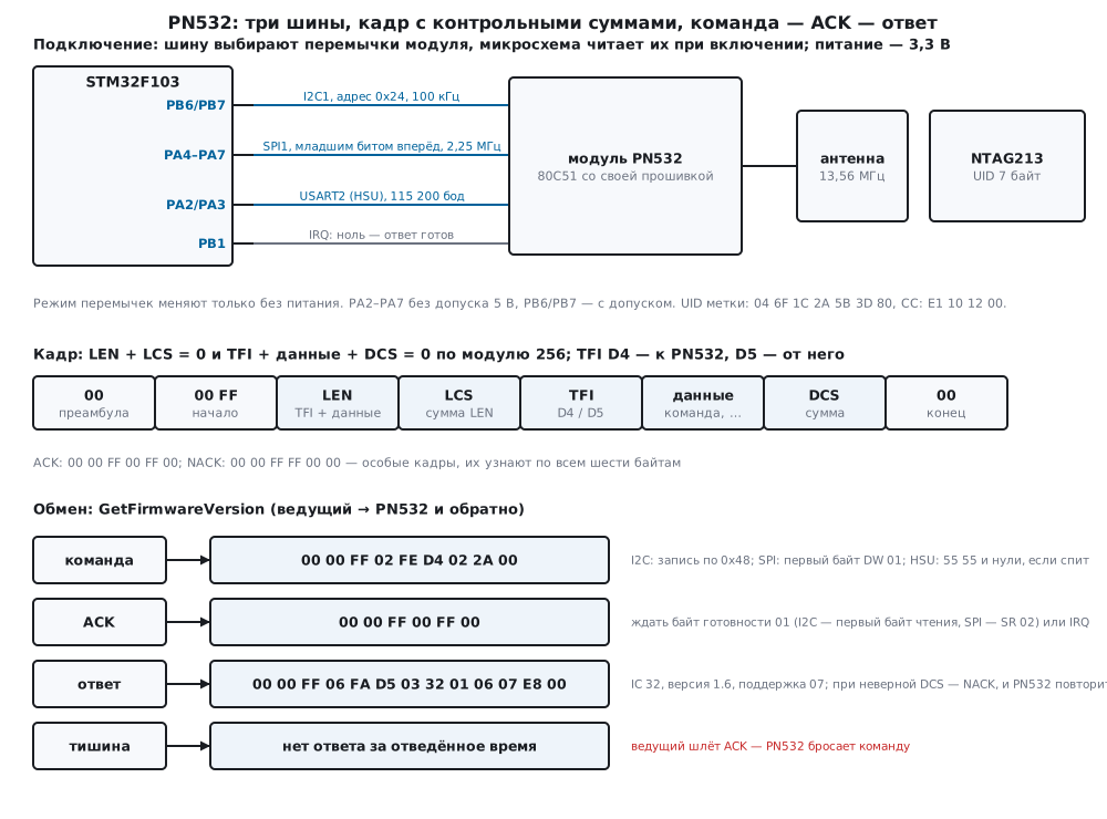
18д.1 How the PN532 differs from the RC522
The MFRC522 from section 18г exposes registers: the FIFO, flags, a timer, a CRC coprocessor. Everything else, REQA, anticollision, UID cascades, SELECT, CRC_A checking, is done by the firmware of our microcontroller. The PN532 has an 80C51 core of its own with firmware in ROM (per the manufacturer's documentation, not checked), and that core does all this work. The host gives the InListPassiveTarget command and gets a ready UID, ATQA and SAK in one answer.
The price is a different protocol. There are no registers, there are frames: a command goes out in a frame with a length and two checksums, the PN532 first confirms reception with an ACK frame, then, when the work is done, gives the answer. While there is no answer, the host waits: it polls the ready byte or watches the IRQ pin.
| RC522 (section 18г) | PN532 | |
|---|---|---|
| what the firmware talks to | MFRC522 registers | PN532 firmware commands |
| anticollision, CRC_A | in our firmware | inside the PN532 |
| buses | SPI on the modules | I²C, SPI or UART, by jumpers |
| reception acknowledgement | none | an ACK frame |
| card emulation | none | TgInitAsTarget |
The same frame travels over all three buses. Only the wrapping changes:
over I²C a ready byte comes before the answer, over SPI every transaction
starts with a service byte, over UART the chip is first woken up. The
driver of this section pn18f.c hides the wrapping in three small
functions, and the commands above them are shared.
18д.2 The frame: LEN, LCS, TFI, DCS, ACK and NACK
The frame is 00 (preamble), 00 FF (start), LEN, LCS, TFI, data, DCS,
00 (end). LEN counts TFI and the data. LCS is chosen so that
LEN + LCS = 0 modulo 256; DCS so that TFI + data + DCS = 0. TFI tells
where the frame goes: D4 from the host to the PN532, D5 back. The first
data byte is the command code, in the answer it is the code plus one.
uint32_t pn_frame(uint8_t *out, uint8_t tfi, const uint8_t *d, uint32_t n)
{
    uint32_t len = n + 1u, k = 0;       /* LEN считает TFI и данные */
    uint8_t sum = tfi;
    out[k++] = 0x00;                    /* преамбула */
    out[k++] = 0x00;                    /* код начала: 00 FF */
    out[k++] = 0xFF;
    if (len <= 254u) {
        out[k++] = (uint8_t)len;
        out[k++] = (uint8_t)(0x100u - len);              /* LCS: LEN + LCS = 0 по модулю 256 */
    } else {                            /* расширенный кадр: FF FF LENM LENL LCS */
        out[k++] = 0xFF;
        out[k++] = 0xFF;
        out[k++] = (uint8_t)(len >> 8);
        out[k++] = (uint8_t)len;
        out[k++] = (uint8_t)(0x100u - ((len >> 8) + (len & 0xFFu)));
    }
    out[k++] = tfi;
    for (uint32_t i = 0; i < n; i++) {
        out[k++] = d[i];
        sum = (uint8_t)(sum + d[i]);
    }
    out[k++] = (uint8_t)(0x100u - sum);                  /* DCS: TFI + данные + DCS = 0 по модулю 256 */
    out[k++] = 0x00;                    /* постамбула */
    return k;
}
Examples from the run; the C driver and an independent calculation in Python gave the same:
| command | frame |
|---|---|
| GetFirmwareVersion | 00 00 FF 02 FE D4 02 2A 00 |
| SAMConfiguration | 00 00 FF 05 FB D4 14 01 14 01 02 00 |
| InListPassiveTarget | 00 00 FF 04 FC D4 4A 01 00 E1 00 |
| answer to GetFirmwareVersion | 00 00 FF 06 FA D5 03 32 01 06 07 E8 00 |
For GetFirmwareVersion LEN = 2 (TFI and the code 02), LCS = FE;
D4 + 02 = D6, and DCS = 2A. Another 200 random frames with 1 to 259 data
bytes were built the same way by C and Python, and the driver parsed them
back, all 200.
ACK and NACK. ACK is 00 00 FF 00 FF 00: the PN532 uses it to say "frame
received", and the host to say "drop the current command". NACK is
00 00 FF FF 00 00: the host asks to repeat the last answer. These are
special frames: in both LEN + LCS = FF, not 0, and the normal frame parser
rejects them as frames with a wrong checksum. So the driver recognises ACK
by all six bytes at once. The error frame is 00 00 FF 01 FF 7F 81 00:
one data byte 7F without TFI; in the model the PN532 answers an unknown
command like this (FE, frame 00 00 FF 02 FE D4 FE 2E 00).
The extended frame. LEN in a normal frame is one byte. When there is
more data, 00 FF is followed by FF FF, two length bytes (high first)
and LCS over them. The driver switches to the extended frame when LEN is
above 254 (the limit is per the manufacturer's documentation, not checked):
a frame with 260 data bytes has LEN 261 = 01 05, starts with
00 00 FF FF FF 01 05 FA D4, 271 bytes in total.
Checking the answer. An answer frame with one corrupted bit is caught by the DCS, one with a corrupted length by the LCS. Both cases in the run gave "wrong checksum", and the driver asks for a repeat with a NACK frame (18д.6).
18д.3 Three buses: I²C, SPI and HSU
The bus is chosen by jumpers or switches on the module; the chip reads them once, at power-on (per the manufacturer's documentation, not checked).
I²C. The address is 0x24, on the line 0x48 for writing and 0x49
for reading (about the shifted address see section 17.2). A command is an
ordinary write of the frame. The answer is read differently from sensors:
the first byte of any read is the ready byte, 01 means the frame is
ready. The driver reads one byte until it sees 01, then reads the ready
byte and the frame in one read. I2C1 of the F103 is on PB6 and PB7
(p. 185), open drain (table 27, p. 167), 100 kHz: FREQ = 36,
CCR = 180, TRISE = 37 with APB1 at 36 MHz.
SPI. Every transaction starts with a service byte: 01 writes a frame
(DW), 02 reads the ready byte (SR), 03 reads a frame (DR). The bytes go
least significant bit first. The F103 SPI has the LSBFIRST bit for
this (bit 7 of SPI_CR1, p. 743), and the block itself changes the bit
order, the driver does not see it. Mode 0, divider 32 (BR = 100):
72 MHz / 32 = 2.25 MHz, with a margin from 5 MHz, the PN532 SPI limit per
the manufacturer's documentation (not checked).
    SPI1->CR1 = SPI_CR1_MSTR | SPI_BR | SPI_CR1_LSBFIRST | SPI_CR1_SSM | SPI_CR1_SSI;   /* режим 0 */
    SPI1->CR1 |= SPI_CR1_SPE;
HSU is the module's UART, 115 200 baud by default. There is no ready
byte: frames simply arrive as a stream, and the driver reads five header
bytes and then as many as LEN says. But after power-on and after sleep the
PN532 has to be woken up over UART: before the first command the driver
sends 55 55 and 14 zeros. USART2 of the F103 is PA2 and PA3 (p. 185), on
APB1 at 36 MHz BRR = 313.
Readiness. One function for two buses and for the IRQ pin:
static int ready(pn_t *p)
{
    uint8_t tx[2] = {PN_SPI_SR, 0}, rx[2] = {0, 0}, st = 0;
    if (p->use_irq)
        return pn_irq() == 0;           /* IRQ вниз — ответ готов */
    if (p->bus == PN_BUS_I2C)
        return pn_i2c_read(p->i2c_addr, &st, 1) == 0 && (st & 0x01u);
    pn_spi(tx, rx, 2);
    return rx[1] & 0x01u;
}
One GetFirmwareVersion command on three buses in the model (ACK is ready 0.5 ms after the frame, the answer another 1 ms later; these are model assumptions):
| bus | operations | bytes on the bus | time |
|---|---|---|---|
| I²C, 100 kHz, polling | 6 | 39 | 4.63 ms |
| I²C, IRQ | 3 | 33 | 4.03 ms |
| SPI, 2.25 MHz, polling | 7 | 39 | 2.139 ms |
| SPI, IRQ | 3 | 31 | 2.11 ms |
| HSU, 115 200 baud | 5 | 28 | 3.41 ms |
Over I²C the 39 bytes are the frame write with the address (10), three polls of 2 bytes, the ACK with the ready byte and the address (8) and the answer (15). The IRQ pin takes the polls off the bus: the same 3 readiness checks go through the PB1 pin, and 33 bytes remain on the bus.
18д.4 Finding a tag: SAMConfiguration, GetFirmwareVersion, InListPassiveTarget
pn_begin gives two commands. SAMConfiguration 14 01 14 01 is the
normal mode without an external security module and with the IRQ pin on
(per the manufacturer's documentation, not checked); the answer is the code
15. GetFirmwareVersion 02 answers 03 32 01 06 07: chip 32
(PN532), version 1.6, 07 says which tag types are supported. This is how
the model repeats the manufacturer's description (not checked); a real chip
may report another version. If there is no answer at all, there is no point
going further: the bus, the jumpers or the power (18д.7).
InListPassiveTarget 4A 01 00 finds one tag at 106 kbit/s, type A.
The PN532 itself sends REQA, runs the anticollision over the cascades,
checks CRC_A and selects the tag, all that was our code in section 18г.
The answer for an NTAG213 tag in the model:
00 00 FF 0F F1 D5 4B 01 01 00 44 00 07 04 6F 1C 2A 5B 3D 80 C2 00
After D5 4B: one tag (01), its number for the following commands
(01), ATQA 00 44, SAK 00, the UID length 07 and the UID itself
04 6F 1C 2A 5B 3D 80. The PN532 gives ATQA with the high byte first; in
the air, as in 18г, it is 44 00 (the order is per the manufacturer's
documentation, not checked). The search took 6.217 ms over SPI. The MIFARE
Classic 1K card from section 18г gave over I²C ATQA 00 04, SAK 08 and
UID 3A 9F 12 C4 of 4 bytes in 9.49 ms.
How long to search. By default the PN532 searches for a tag forever:
the MaxRetries parameter of passive activation is FF (per the
manufacturer's documentation, not checked; so in the model). The
RFConfiguration command 32 05 FF 01 nn limits the number of
attempts: the firmware of this section sets 10. What happens without it
is in 18д.6.
18д.5 NTAG213 and NTAG215: pages, READ and WRITE, a link in NDEF
NTAG21x tags are descendants of MIFARE Ultralight: memory of 4-byte pages,
without keys or a cipher. NTAG213 has 45 pages, NTAG215 has 135 (so in the
Flipper Zero sources, mf_ultralight.c). Tag commands go through
InDataExchange 40 01 …: the PN532 passes them to tag number 1 and
returns the answer with a status byte, 00 means success.
- READ
30 n: 16 bytes, pages n, n+1, n+2, n+3. - WRITE
A2 nand 4 bytes: one page.
Pages 0–2 are the UID, two BCC checksums and lock bytes:
04 6F 1C FF | 2A 5B 3D 80 | CC 48 00 00. BCC0 = 88 ⊕ 04 ⊕ 6F ⊕ 1C = FF,
BCC1 = 2A ⊕ 5B ⊕ 3D ⊕ 80 = CC, the same formula as in Flipper Zero.
Page 3 is the CC: E1 10 12 00. E1 means the tag is formatted for NDEF,
10 is version 1.0, 12 is the data area size in units of eight bytes:
18 · 8 = 144 bytes, pages 4–39. The NTAG215 CC is E1 10 3E 00,
62 · 8 = 496 bytes.
One READ from address 3 brings both the CC and the start of the data,
ntag_read in 4.21 ms:
E1 10 12 00 01 03 A0 0C 34 03 00 FE 00 00 00 00
This is the factory layout of the NTAG213 (the same as in the Flipper Zero
tag generator): TLV 01 of length 3, where the lock bits are, an empty
NDEF message 03 00 and the end FE. The NTAG215 has just 03 00 FE.
A link in NDEF. The NDEF message lies in TLV 03. A link record is the
header D1 (first and last record, short, NFC Forum type), type length 1,
the data length, type U, the prefix code and the rest of the address.
Prefixes are encoded by a number: 01 is http://www., 02 is
https://www., 03 is http://, 04 is https://. For the address
https://example.com/pn532 ndef_uri gave 25 bytes:
03 16 D1 01 12 55 04 65 78 61 6D 70 6C 65 2E 63 6F 6D 2F 70 6E 35 33 32 FE
The record length 16 = 22: 4 header bytes and 18 data bytes, the code
04 and 17 letters example.com/pn532.
    while (i < have && m[i] != 0x03u && m[i] != 0xFEu) {   /* пропустить TLV блокировок и памяти */
        if (m[i] == 0x00u) {
            i++;
            continue;
        }
        i += 2u + m[i + 1u];
    }
    at = i;                             /* сюда ляжет новое сообщение; TLV до него не трогаем */
ntag_write_url reads the CC, skips TLV 01 and puts the message from
offset 5, from the second byte of page 5. The first byte of that page,
34 from the lock TLV, the driver rewrites with the same value. 7 pages
(5–11) were written in 8 commands, one READ and seven WRITE, 54.529 ms; in
the model writing a page takes 6 ms, this is an assumption. Back,
ntag_read_url read the link with three READ in 12.629 ms, and an
independent parse of the tag memory in Python found the same address.
A long link. An address of 300 characters does not fit a short record:
the data is 293 bytes, more than 255. Then the header is C1 (without the
short record flag), and the data length takes 4 bytes; the record is 300
bytes, and the TLV length does not fit a byte either: 03 FF 01 2C. On the
NTAG215 this made 305 bytes, 77 pages, 557.72 ms; reading back took 20
commands, 84.196 ms. On the NTAG213 the same link does not fit into 144
bytes, and the driver refuses to write without touching the tag.
18д.6 MIFARE Classic, card emulation, timeouts and sleep
MIFARE Classic through the PN532. The same card commands as in section
18г go through InDataExchange: authentication 60 with the block number,
6 bytes of the key and the UID, then READ 30, 16 bytes. The PN532 runs
the Crypto1 cipher itself, like the MFRC522. Everything said in 18г.6
still holds: MIFARE Classic and the UID are not fit for security, whatever
reader is used. The bench model only finds Classic, it does not read it.
Card emulation. With the TgInitAsTarget command (8C) the PN532 itself
pretends to be a tag: it answers a reader, a phone for example, and
exchanges data with it through the TgGetData and TgSetData commands. This
is how a "phone to device" exchange is done without a separate tag. Per the
manufacturer's documentation, part of the UID is then set by the chip
itself, and a copy of someone else's card cannot be made this way (not
checked). The driver of this section has no emulation, and it was not
modelled.
Timeouts. Every command waits 10 ms for the ACK, and for the answer as long as it is given. If there is no answer, the driver sends ACK: the PN532 drops the command and is ready for the next one. In the model a search without a tag with the factory number of attempts never ended: the driver waited 100 ms and sent ACK, 124.09 ms and 103 polls, and the following GetFirmwareVersion command went through as usual. With RFConfiguration set to 5 retries the same search returned "no tags" in 16.69 ms.
A wrong checksum. In the model one bit of the GetFirmwareVersion answer
flipped on the line: D5 13 instead of D5 03. The DCS did not match, the
driver sent NACK, the PN532 repeated the answer, and the command went
through with one repeat in 3.228 ms instead of 2.139 ms.
Sleep. PowerDown 16 B0 puts the PN532 to sleep with wake-up by I²C,
SPI and UART (the wake-up bits are per the manufacturer's documentation,
not checked). How it wakes up in the model:
| bus | how the driver wakes it | GetFirmwareVersion after sleep | without wake-up |
|---|---|---|---|
| I²C | the first address is not acknowledged, a repeat after 1 ms | 6.55 ms | bus error: address without ACK |
| SPI | an empty transaction and a 1 ms pause | 3.146 ms | no ACK, 10.114 ms |
| HSU | 55 55 and zeros before the frame |
4.799 ms | no ACK, 10.781 ms |
The wake-up behaviour over I²C and SPI is a model assumption: there is no document. The conclusion of the table does not depend on the details: after sleep the first exchange is lost, and the driver has to expect it.
18д.7 Pitfalls
The PN532 is silent: the wrong bus. The jumpers are set to HSU, and the
firmware talks I²C: the address is not acknowledged, pn_begin returns a
bus error. Moving the jumpers on a running module is not enough: in the
model after the move the answer is the same, and only after power off and
on pn_begin, SAMConfiguration and GetFirmwareVersion, goes through in
9.17 ms.
The PN532 is silent: the wrong SPI bit order. Without LSBFIRST the SPI
block sends bytes most significant bit first, and the PN532 sees the byte
80 instead of DW 01, and 40 instead of SR 02. That is what happened
in the model: not a single understood transaction, no ACK after 10.124 ms.
If an SPI block cannot do least significant bit first, the bytes are
reversed in software; the F103 has the bit.
A wrong I²C address. 0x48 is already the shifted address. With it the
driver got NACK on the address three times, 5.76 ms and a bus error; with
0x24 the answer came in 4.63 ms.
A module powered from 5 V. The PN532 is a 3.3 V chip. Many modules carry their own regulator and pull I²C up to their own supply (per sellers' descriptions, not checked). PB6 and PB7 of the F103 withstand 5 V (p. 32), PA2–PA7 do not (p. 29): over SPI and UART the module is powered only from 3.3 V.
Long wires. A line error is caught by LCS and DCS; the driver answers a wrong-checksum answer with NACK instead of accepting it (18д.6). But a command that was not received looks like "no ACK", and after dozens of centimetres of wire on I²C and SPI it is better to lower the frequency.
A skipped ACK. If the ACK is not read and the host waits for the answer right away, over I²C and SPI the host reads the ACK instead of the answer. A hung command, a search without a tag for example, is dropped with an ACK frame from the host; without it the PN532 is busy with it (per the manufacturer's documentation, not checked).
A search without end. Without RFConfiguration InListPassiveTarget without a tag never answers: the firmware waits until its own timeout, and without one it hangs.
18д.8 Summary
- The PN532 is an 80C51 with its own firmware: commands and answers instead of registers; it does anticollision and CRC_A itself.
- The frame:
00 00 FF LEN LCS D4 … DCS 00; GetFirmwareVersion is00 00 FF 02 FE D4 02 2A 00, the answer is03 32 01 06 07. - ACK
00 00 FF 00 FF 00, NACK00 00 FF FF 00 00; the extended frame is for LEN above 254. - I²C: address
0x24, ready byte01; SPI: DW01, SR02, DR03, least significant bit first, 2.25 MHz; HSU: 115 200 baud, wake-up55 55. - IRQ removes the polls: over I²C 39 bytes → 33.
- InListPassiveTarget: NTAG213 gives ATQA
00 44, SAK00, a UID of 7 bytes, 6.217 ms over SPI. - NTAG213: 45 pages, CC
E1 10 12 00, 144 bytes; NTAG215: 135 pages, 496 bytes. - The link
https://example.com/pn532— a TLV of 25 bytes, 7 pages, 54.529 ms. - Without RFConfiguration a search without a tag never ends; timeout, then ACK.
Full sources
pn18f.h — PN532 commands and answers, the frame, the driver and platform interface.
/* pn18f.h — раздел 18д: драйвер NFC-модуля PN532 без регистров STM32.
 * Драйвер говорит с микросхемой кадрами через функции платформы: I2C, SPI или UART (HSU) — что выбрано перемычками.
 * В прошивке fw18f.c их даёт STM32F103, в стенде host18f.c — модель model18f.py.
 * Формат кадра, коды команд и ответов PN532 — по документации производителя (в проекте её нет, не проверено);
 * команды NTAG2xx и разметка NDEF сверены с исходниками прошивки Flipper Zero (выдержки — flipper_ntag.txt). */
#ifndef PN18F_H
#define PN18F_H
#include <stdint.h>

/* ── кадр ─────────────────────────────────────────────────────────────── */
#define PN_TFI_HOST   0xD4u             /* кадр от ведущего к PN532 */
#define PN_TFI_CHIP   0xD5u             /* кадр от PN532 к ведущему */
#define PN_I2C_ADDR   0x24u             /* семибитный адрес: в линии 0x48 — запись, 0x49 — чтение */
#define PN_SPI_DW     0x01u             /* первый байт SPI: запись данных */
#define PN_SPI_SR     0x02u             /* чтение байта готовности */
#define PN_SPI_DR     0x03u             /* чтение данных */
#define PN_MAXDATA    265u              /* TFI и данные расширенного кадра — с запасом */
#define PN_FRAME_MAX  (PN_MAXDATA + 10u)

/* ── команды PN532 ────────────────────────────────────────────────────── */
#define PN_GETFW      0x02u             /* GetFirmwareVersion */
#define PN_SAMCONFIG  0x14u             /* SAMConfiguration */
#define PN_POWERDOWN  0x16u
#define PN_RFCONFIG   0x32u             /* RFConfiguration */
#define PN_INEXCHANGE 0x40u             /* InDataExchange */
#define PN_INLIST     0x4Au             /* InListPassiveTarget */
#define PN_INRELEASE  0x52u
#define PN_TGINIT     0x8Cu             /* TgInitAsTarget — эмуляция карты, в драйвере не используется */

/* ── команды метки NTAG2xx ────────────────────────────────────────────── */
#define NTAG_READ     0x30u             /* 16 байт: четыре страницы по 4 байта */
#define NTAG_WRITE    0xA2u             /* одна страница: 4 байта */

/* ── ответ драйвера ───────────────────────────────────────────────────── */
enum { PN_OK, PN_TIMEOUT, PN_NOACK, PN_FRAME, PN_CHECKSUM, PN_ERRFRAME, PN_BUS, PN_STATUS, PN_NOTAG, PN_NOSPACE, PN_NDEF };
enum { PN_BUS_I2C = 1, PN_BUS_SPI, PN_BUS_HSU };

extern const uint8_t PN_ACK[6], PN_NACK[6];

typedef struct {
    uint8_t sens_res[2];                /* ATQA — так, как его отдаёт PN532 */
    uint8_t sel_res;                    /* SAK */
    uint8_t uid[10];
    uint8_t uid_len;
} pn_tag_t;

typedef struct {
    uint8_t bus;                        /* PN_BUS_I2C, PN_BUS_SPI или PN_BUS_HSU */
    uint8_t i2c_addr;                   /* 0x24; другое — опыт с неверным адресом */
    uint8_t use_irq;                    /* 1 — ждать готовность по выводу IRQ, а не опросом шины */
    uint8_t no_wake;                    /* 1 — не будить после сна (опыт «PN532 молчит») */
    uint8_t asleep;                     /* драйвер считает, что микросхема спит */
    uint8_t fw[4];                      /* IC, Ver, Rev, Support из GetFirmwareVersion */
    uint8_t status;                     /* байт состояния последнего InDataExchange */
    uint32_t polls, nacks, retries, aborts, wakes, reads, writes;
} pn_t;

/* ── платформа: даёт прошивка или стенд ───────────────────────────────── */
int pn_i2c_write(uint8_t addr7, const uint8_t *d, uint32_t n);   /* 0 — адрес и все байты подтверждены */
int pn_i2c_read(uint8_t addr7, uint8_t *d, uint32_t n);          /* 0 — адрес подтверждён */
void pn_spi(const uint8_t *tx, uint8_t *rx, uint32_t n);         /* NSS вниз, n байт младшим битом вперёд, NSS вверх */
void pn_uart_write(const uint8_t *d, uint32_t n);
uint32_t pn_uart_read(uint8_t *d, uint32_t n, uint32_t timeout_ms);   /* сколько байт пришло */
int pn_irq(void);                                                /* уровень IRQ: 0 — есть что читать */
void pn_delay_ms(uint32_t ms);

/* ── кадры ────────────────────────────────────────────────────────────── */
uint32_t pn_frame(uint8_t *out, uint8_t tfi, const uint8_t *d, uint32_t n);   /* -> длина кадра */
int pn_unframe(const uint8_t *f, uint32_t n, uint8_t *d, uint32_t *dn);       /* d — TFI и данные */

/* ── команды ──────────────────────────────────────────────────────────── */
int pn_cmd(pn_t *p, const uint8_t *cmd, uint32_t n, uint8_t *resp, uint32_t *rn, uint32_t rmax, uint32_t timeout_ms);
void pn_abort(pn_t *p);
int pn_begin(pn_t *p, uint8_t bus);
int pn_getfw(pn_t *p);
int pn_sam(pn_t *p);
int pn_retries(pn_t *p, uint8_t passive);
int pn_list(pn_t *p, pn_tag_t *t, uint32_t timeout_ms);
int pn_exchange(pn_t *p, const uint8_t *tx, uint32_t n, uint8_t *rx, uint32_t *rn, uint32_t rmax);
int pn_release(pn_t *p);
int pn_sleep(pn_t *p);

/* ── NTAG2xx и NDEF ───────────────────────────────────────────────────── */
int ntag_read(pn_t *p, uint8_t page, uint8_t out[16]);
int ntag_write(pn_t *p, uint8_t page, const uint8_t d[4]);
uint32_t ndef_uri(uint8_t *out, uint32_t cap, const char *url);              /* TLV 03 … FE -> длина или 0 */
int ndef_parse(const uint8_t *m, uint32_t n, char *url, uint32_t cap, uint32_t *tlv_at);
int ntag_write_url(pn_t *p, const char *url, uint32_t *pages);
int ntag_read_url(pn_t *p, char *url, uint32_t cap);

#endif
pn18f.c — the driver without STM32 registers: shared by the firmware and the bench.
/* pn18f.c — раздел 18д: драйвер PN532 — кадры с LCS и DCS, ACK и NACK, обёртки I2C, SPI и HSU, ожидание
 * готовности опросом или по IRQ, команды SAMConfiguration, GetFirmwareVersion, RFConfiguration,
 * InListPassiveTarget, InDataExchange, InRelease, PowerDown; страницы NTAG2xx и запись URL в NDEF. Без регистров STM32. */
#include <string.h>
#include "pn18f.h"

#define ACK_MS 10u                      /* ждать ACK, мс */
#define RESEND 2u                       /* сколько раз просить повтор (NACK) при неверной сумме */

const uint8_t PN_ACK[6] = {0x00, 0x00, 0xFF, 0x00, 0xFF, 0x00};
const uint8_t PN_NACK[6] = {0x00, 0x00, 0xFF, 0xFF, 0x00, 0x00};
static const uint8_t WAKE[16] = {0x55, 0x55};          /* HSU: 55 55 и нули — разбудить перед первой командой */

/* ── кадр: 00 00 FF LEN LCS TFI данные DCS 00 ─────────────────────────── */
uint32_t pn_frame(uint8_t *out, uint8_t tfi, const uint8_t *d, uint32_t n)
{
    uint32_t len = n + 1u, k = 0;       /* LEN считает TFI и данные */
    uint8_t sum = tfi;
    out[k++] = 0x00;                    /* преамбула */
    out[k++] = 0x00;                    /* код начала: 00 FF */
    out[k++] = 0xFF;
    if (len <= 254u) {
        out[k++] = (uint8_t)len;
        out[k++] = (uint8_t)(0x100u - len);              /* LCS: LEN + LCS = 0 по модулю 256 */
    } else {                            /* расширенный кадр: FF FF LENM LENL LCS */
        out[k++] = 0xFF;
        out[k++] = 0xFF;
        out[k++] = (uint8_t)(len >> 8);
        out[k++] = (uint8_t)len;
        out[k++] = (uint8_t)(0x100u - ((len >> 8) + (len & 0xFFu)));
    }
    out[k++] = tfi;
    for (uint32_t i = 0; i < n; i++) {
        out[k++] = d[i];
        sum = (uint8_t)(sum + d[i]);
    }
    out[k++] = (uint8_t)(0x100u - sum);                  /* DCS: TFI + данные + DCS = 0 по модулю 256 */
    out[k++] = 0x00;                    /* постамбула */
    return k;
}

int pn_unframe(const uint8_t *f, uint32_t n, uint8_t *d, uint32_t *dn)
{
    uint32_t i = 0, len;
    while (i + 1u < n && !(f[i] == 0x00 && f[i + 1u] == 0xFF))
        i++;                            /* преамбул бывает сколько угодно: ищем 00 FF */
    i += 2u;
    if (i + 2u > n)
        return PN_FRAME;
    if (f[i] == 0xFF && f[i + 1u] == 0xFF) {             /* расширенный */
        if (i + 5u > n || (uint8_t)(f[i + 2u] + f[i + 3u] + f[i + 4u]) != 0)
            return PN_CHECKSUM;
        len = (uint32_t)f[i + 2u] << 8 | f[i + 3u];
        i += 5u;
    } else {
        if ((uint8_t)(f[i] + f[i + 1u]) != 0)
            return PN_CHECKSUM;         /* LCS не сошёлся (у NACK тоже: FF + 00) */
        len = f[i];
        i += 2u;
    }
    if (len == 0u || len > PN_MAXDATA || i + len + 1u > n)
        return PN_FRAME;
    uint8_t sum = 0;
    for (uint32_t k = 0; k <= len; k++)
        sum = (uint8_t)(sum + f[i + k]);
    if (sum != 0)
        return PN_CHECKSUM;             /* DCS не сошёлся */
    memcpy(d, f + i, len);
    *dn = len;
    if (len == 1u && d[0] == 0x7Fu)
        return PN_ERRFRAME;             /* кадр ошибки 00 00 FF 01 FF 7F 81 00 */
    return PN_OK;
}

/* ── шина ─────────────────────────────────────────────────────────────── */
static int bus_write(pn_t *p, const uint8_t *f, uint32_t n)
{
    static uint8_t tx[PN_FRAME_MAX + 1u], rx[PN_FRAME_MAX + 1u];
    p->writes++;
    if (p->bus == PN_BUS_I2C) {
        for (uint32_t t = 0; t < 3u; t++) {                /* после сна первый адрес будит и теряется */
            if (pn_i2c_write(p->i2c_addr, f, n) == 0)
                return PN_OK;
            if (p->no_wake)
                break;
            p->retries++;
            pn_delay_ms(1);
        }
        return PN_BUS;
    }
    if (p->bus == PN_BUS_SPI) {
        tx[0] = PN_SPI_DW;
        memcpy(tx + 1, f, n);
        pn_spi(tx, rx, n + 1u);
        return PN_OK;
    }
    pn_uart_write(f, n);
    return PN_OK;
}

static void wake(pn_t *p)
{
    uint8_t tx[2] = {PN_SPI_SR, 0}, rx[2];
    if (!p->asleep)
        return;
    p->asleep = 0;
    if (p->no_wake)
        return;
    p->wakes++;
    if (p->bus == PN_BUS_HSU) {
        pn_uart_write(WAKE, sizeof WAKE);
    } else if (p->bus == PN_BUS_SPI) {
        pn_spi(tx, rx, 2);              /* NSS вниз будит; эта транзакция теряется */
        pn_delay_ms(1);
    }                                   /* I2C: будит первый адрес, его повторяет bus_write */
}

static int ready(pn_t *p)
{
    uint8_t tx[2] = {PN_SPI_SR, 0}, rx[2] = {0, 0}, st = 0;
    if (p->use_irq)
        return pn_irq() == 0;           /* IRQ вниз — ответ готов */
    if (p->bus == PN_BUS_I2C)
        return pn_i2c_read(p->i2c_addr, &st, 1) == 0 && (st & 0x01u);
    pn_spi(tx, rx, 2);
    return rx[1] & 0x01u;
}

static int wait_ready(pn_t *p, uint32_t timeout_ms)
{
    for (uint32_t ms = 0;; ms++) {
        p->polls++;
        if (ready(p))
            return PN_OK;
        if (ms >= timeout_ms)
            return PN_TIMEOUT;
        pn_delay_ms(1);
    }
}

/* Прочитать кадр: I2C и SPI — want байт после готовности, HSU — по потоку, сколько скажет LEN. */
static int read_frame(pn_t *p, uint8_t *f, uint32_t want, uint32_t timeout_ms, uint32_t *got)
{
    static uint8_t tx[PN_FRAME_MAX + 1u], rx[PN_FRAME_MAX + 1u];
    p->reads++;
    *got = 0;
    if (p->bus == PN_BUS_HSU) {
        uint32_t k = pn_uart_read(f, 5, timeout_ms), more;
        if (k < 5u)
            return PN_TIMEOUT;
        if (f[3] == 0x00 && f[4] == 0xFF)
            more = 1;                   /* ACK: остался байт 00 */
        else if (f[3] == 0xFF && f[4] == 0xFF) {
            if (pn_uart_read(f + 5, 3, ACK_MS) < 3u)
                return PN_TIMEOUT;
            k = 8;
            more = ((uint32_t)f[5] << 8 | f[6]) + 2u;
        } else
            more = (uint32_t)f[3] + 2u;
        if (k + more > PN_FRAME_MAX || pn_uart_read(f + k, more, ACK_MS) < more)
            return PN_TIMEOUT;
        *got = k + more;
        return PN_OK;
    }
    if (wait_ready(p, timeout_ms) != PN_OK)
        return PN_TIMEOUT;
    if (p->bus == PN_BUS_I2C) {
        if (pn_i2c_read(p->i2c_addr, rx, want + 1u) != 0 || !(rx[0] & 0x01u))
            return PN_BUS;
        memcpy(f, rx + 1, want);        /* первый байт — снова байт готовности */
    } else {
        memset(tx, 0, want + 1u);
        tx[0] = PN_SPI_DR;
        pn_spi(tx, rx, want + 1u);
        memcpy(f, rx + 1, want);
    }
    *got = want;
    return PN_OK;
}

void pn_abort(pn_t *p)
{
    p->aborts++;
    bus_write(p, PN_ACK, 6);            /* ACK от ведущего — «бросить текущую команду» */
}

int pn_cmd(pn_t *p, const uint8_t *cmd, uint32_t n, uint8_t *resp, uint32_t *rn, uint32_t rmax, uint32_t timeout_ms)
{
    static uint8_t f[PN_FRAME_MAX], d[PN_MAXDATA];
    uint32_t got = 0, dn = 0, len = pn_frame(f, PN_TFI_HOST, cmd, n);
    *rn = 0;
    wake(p);
    if (bus_write(p, f, len) != PN_OK)
        return PN_BUS;
    if (read_frame(p, f, 6, ACK_MS, &got) != PN_OK || memcmp(f, PN_ACK, 6) != 0)
        return PN_NOACK;                /* кадр не принят: нет связи, не тот режим, неверная сумма */
    for (uint32_t t = 0; t <= RESEND; t++) {
        int st = read_frame(p, f, rmax + 8u, timeout_ms, &got);
        if (st == PN_TIMEOUT) {
            pn_abort(p);
            return PN_TIMEOUT;
        }
        st = st == PN_OK ? pn_unframe(f, got, d, &dn) : st;
        if (st == PN_ERRFRAME)
            return PN_ERRFRAME;
        if (st != PN_OK) {
            p->nacks++;
            bus_write(p, PN_NACK, 6);   /* NACK — «пришли ответ ещё раз» */
            continue;
        }
        if (dn < 2u || d[0] != PN_TFI_CHIP || d[1] != (uint8_t)(cmd[0] + 1u))
            return PN_FRAME;
        memcpy(resp, d + 1, dn - 1u);   /* код ответа (команда + 1) и данные */
        *rn = dn - 1u;
        return PN_OK;
    }
    return PN_CHECKSUM;
}

/* ── команды ──────────────────────────────────────────────────────────── */
int pn_begin(pn_t *p, uint8_t bus)
{
    memset(p, 0, sizeof *p);
    p->bus = bus;
    p->i2c_addr = PN_I2C_ADDR;
    p->asleep = bus == PN_BUS_HSU;      /* по UART микросхему будят и после включения */
    int st = pn_sam(p);
    return st != PN_OK ? st : pn_getfw(p);
}

int pn_getfw(pn_t *p)
{
    uint8_t c = PN_GETFW, r[8];
    uint32_t n = 0;
    int st = pn_cmd(p, &c, 1, r, &n, 5, 20);
    if (st != PN_OK)
        return st;
    if (n != 5u)
        return PN_FRAME;
    memcpy(p->fw, r + 1, 4);            /* IC, Ver, Rev, Support */
    return PN_OK;
}

int pn_sam(pn_t *p)
{
    uint8_t c[4] = {PN_SAMCONFIG, 0x01, 0x14, 0x01}, r[4];   /* обычный режим, 0x14 × 50 мс, IRQ включён */
    uint32_t n = 0;
    return pn_cmd(p, c, 4, r, &n, 1, 20);
}

int pn_retries(pn_t *p, uint8_t passive)
{
    uint8_t c[5] = {PN_RFCONFIG, 0x05, 0xFF, 0x01, passive}, r[4];   /* MaxRetries: ATR, PSL, пассивная активация */
    uint32_t n = 0;
    return pn_cmd(p, c, 5, r, &n, 1, 20);
}

int pn_list(pn_t *p, pn_tag_t *t, uint32_t timeout_ms)
{
    uint8_t c[3] = {PN_INLIST, 0x01, 0x00}, r[24];          /* одна метка, 106 кбит/с, тип A */
    uint32_t n = 0;
    int st = pn_cmd(p, c, 3, r, &n, 17, timeout_ms);
    if (st != PN_OK)
        return st;
    if (n < 2u || r[1] == 0u)
        return PN_NOTAG;
    if (n < 7u || r[6] > 10u || n < 7u + r[6])
        return PN_FRAME;
    t->sens_res[0] = r[3];
    t->sens_res[1] = r[4];
    t->sel_res = r[5];
    t->uid_len = r[6];
    memcpy(t->uid, r + 7, r[6]);
    return PN_OK;
}

int pn_exchange(pn_t *p, const uint8_t *tx, uint32_t n, uint8_t *rx, uint32_t *rn, uint32_t rmax)
{
    uint8_t c[64], r[64];
    uint32_t k = 0;
    if (n + 2u > sizeof c || rmax + 2u > sizeof r)
        return PN_FRAME;
    c[0] = PN_INEXCHANGE;
    c[1] = 0x01;                        /* номер метки из InListPassiveTarget */
    memcpy(c + 2, tx, n);
    int st = pn_cmd(p, c, n + 2u, r, &k, rmax + 2u, 100);
    *rn = 0;
    if (st != PN_OK)
        return st;
    if (k < 2u)
        return PN_FRAME;
    p->status = r[1];
    if (r[1] & 0x3Fu)
        return PN_STATUS;               /* метка не ответила или отказала */
    memcpy(rx, r + 2, k - 2u);
    *rn = k - 2u;
    return PN_OK;
}

int pn_release(pn_t *p)
{
    uint8_t c[2] = {PN_INRELEASE, 0x00}, r[4];
    uint32_t n = 0;
    return pn_cmd(p, c, 2, r, &n, 2, 20);
}

int pn_sleep(pn_t *p)
{
    uint8_t c[2] = {PN_POWERDOWN, 0xB0}, r[4];               /* будить по I2C, SPI и HSU */
    uint32_t n = 0;
    int st = pn_cmd(p, c, 2, r, &n, 2, 20);
    if (st == PN_OK)
        p->asleep = 1;
    return st;
}

/* ── NTAG2xx ──────────────────────────────────────────────────────────── */
int ntag_read(pn_t *p, uint8_t page, uint8_t out[16])
{
    uint8_t c[2] = {NTAG_READ, page}, r[20];
    uint32_t n = 0;
    int st = pn_exchange(p, c, 2, r, &n, 16);
    if (st != PN_OK)
        return st;
    if (n != 16u)
        return PN_FRAME;
    memcpy(out, r, 16);
    return PN_OK;
}

int ntag_write(pn_t *p, uint8_t page, const uint8_t d[4])
{
    uint8_t c[6] = {NTAG_WRITE, page, d[0], d[1], d[2], d[3]}, r[4];
    uint32_t n = 0;
    return pn_exchange(p, c, 6, r, &n, 0);
}

/* ── NDEF: TLV 03, запись URI (тип «U»), TLV FE ───────────────────────── */
static const char *const PREFIX[5] = {"", "http://www.", "https://www.", "http://", "https://"};

uint32_t ndef_uri(uint8_t *out, uint32_t cap, const char *url)
{
    uint32_t code = 0, best = 0, k = 0;
    for (uint32_t i = 1; i < 5u; i++) {
        uint32_t l = (uint32_t)strlen(PREFIX[i]);
        if (l > best && strncmp(url, PREFIX[i], l) == 0) {
            best = l;
            code = i;
        }
    }
    const char *rest = url + best;
    uint32_t pl = 1u + (uint32_t)strlen(rest);           /* поле полезной нагрузки: код приставки и остаток */
    uint32_t rec = (pl <= 255u ? 4u : 7u) + pl;          /* заголовок, длина типа, длина нагрузки, тип «U» */
    uint32_t tlv = (rec <= 254u ? 2u : 4u) + rec + 1u;
    if (tlv > cap)
        return 0;
    out[k++] = 0x03;                    /* TLV: сообщение NDEF */
    if (rec <= 254u) {
        out[k++] = (uint8_t)rec;
    } else {
        out[k++] = 0xFF;                /* длинная длина: FF и два байта */
        out[k++] = (uint8_t)(rec >> 8);
        out[k++] = (uint8_t)rec;
    }
    out[k++] = pl <= 255u ? 0xD1u : 0xC1u;               /* MB, ME, (SR), TNF = 1 — тип NFC Forum */
    out[k++] = 0x01;                    /* длина типа */
    if (pl <= 255u) {
        out[k++] = (uint8_t)pl;
    } else {
        out[k++] = 0;
        out[k++] = 0;
        out[k++] = (uint8_t)(pl >> 8);
        out[k++] = (uint8_t)pl;
    }
    out[k++] = 'U';
    out[k++] = (uint8_t)code;
    memcpy(out + k, rest, pl - 1u);
    k += pl - 1u;
    out[k++] = 0xFE;                    /* TLV: конец */
    return k;
}

int ndef_parse(const uint8_t *m, uint32_t n, char *url, uint32_t cap, uint32_t *tlv_at)
{
    uint32_t i = 0;
    while (i < n) {
        uint8_t t = m[i];
        if (t == 0x00) {                /* заполнитель: без длины */
            i++;
            continue;
        }
        if (t == 0xFE || i + 2u > n)
            return PN_NDEF;             /* конец, а сообщения NDEF не было */
        uint32_t len = m[i + 1u], h = 2;
        if (len == 0xFFu) {
            if (i + 4u > n)
                return PN_NDEF;
            len = (uint32_t)m[i + 2u] << 8 | m[i + 3u];
            h = 4;
        }
        if (t != 0x03) {                /* 01 — блокировки, 02 — память, FD — своё: пропустить */
            i += h + len;
            continue;
        }
        *tlv_at = i;
        const uint8_t *r = m + i + h;
        if (i + h + len > n || len < 4u || (r[0] & 0x07u) != 0x01u || r[1] != 1u)
            return PN_NDEF;             /* нужен тип NFC Forum с однобуквенным именем */
        uint32_t pl, j;
        if (r[0] & 0x10u) {             /* SR: длина нагрузки — один байт */
            pl = r[2];
            j = 3;
        } else {
            pl = (uint32_t)r[2] << 24 | (uint32_t)r[3] << 16 | (uint32_t)r[4] << 8 | r[5];
            j = 6;
        }
        if (r[0] & 0x08u)
            j++;                        /* IL: есть длина идентификатора (пропускаем; у нас 0) */
        if (j + 1u + pl > len || r[j] != 'U' || pl < 1u || r[j + 1u] > 4u)
            return PN_NDEF;
        const char *pre = PREFIX[r[j + 1u]];
        uint32_t lp = (uint32_t)strlen(pre);
        if (lp + pl > cap)
            return PN_NOSPACE;
        memcpy(url, pre, lp);
        memcpy(url + lp, r + j + 2u, pl - 1u);
        url[lp + pl - 1u] = 0;
        return PN_OK;
    }
    return PN_NDEF;
}

/* Память метки с 4-й страницы: читает по 16 байт, пока не найдёт TLV FE или не дойдёт до конца области. */
static int user_area(pn_t *p, uint8_t *m, uint32_t *size, uint32_t *have)
{
    uint8_t b[16];
    int st = ntag_read(p, 3, b);        /* страница 3 — CC, за ней сразу страницы 4–6 */
    if (st != PN_OK)
        return st;
    if (b[0] != 0xE1u || b[1] != 0x10u)
        return PN_NDEF;                 /* метка не размечена под NDEF */
    *size = b[2] * 8u;                  /* NTAG213: 0x12 × 8 = 144 байта */
    memcpy(m, b + 4, 12);
    *have = 12;
    while (*have < *size && !memchr(m, 0xFE, *have)) {
        if ((st = ntag_read(p, (uint8_t)(4u + *have / 4u), b)) != PN_OK)
            return st;
        memcpy(m + *have, b, 16);
        *have += 16u;
    }
    if (*have > *size)
        *have = *size;
    return PN_OK;
}

int ntag_read_url(pn_t *p, char *url, uint32_t cap)
{
    static uint8_t m[1024];
    uint32_t size = 0, have = 0, at = 0;
    int st = user_area(p, m, &size, &have);
    return st != PN_OK ? st : ndef_parse(m, have, url, cap, &at);
}

int ntag_write_url(pn_t *p, const char *url, uint32_t *pages)
{
    static uint8_t m[1024], t[1024];
    uint32_t size = 0, have = 0, at = 0, i = 0;
    *pages = 0;
    int st = user_area(p, m, &size, &have);
    if (st != PN_OK)
        return st;
    while (i < have && m[i] != 0x03u && m[i] != 0xFEu) {   /* пропустить TLV блокировок и памяти */
        if (m[i] == 0x00u) {
            i++;
            continue;
        }
        i += 2u + m[i + 1u];
    }
    at = i;                             /* сюда ляжет новое сообщение; TLV до него не трогаем */
    uint32_t n = ndef_uri(t, sizeof t, url);
    if (n == 0u || at + n > size)
        return PN_NOSPACE;
    uint32_t first = at / 4u, last = (at + n - 1u) / 4u;
    memcpy(m + at, t, n);               /* байты страницы до at остаются прежними */
    memset(m + at + n, 0, (last + 1u) * 4u - (at + n));
    for (uint32_t pg = first; pg <= last; pg++) {
        if ((st = ntag_write(p, (uint8_t)(4u + pg), m + pg * 4u)) != PN_OK)
            return st;
        (*pages)++;
    }
    return PN_OK;
}
fw18f.c — STM32F103 firmware: I2C1, SPI1 or USART2, output to USART1.
/* fw18f.c — раздел 18д: NFC-модуль PN532 на STM32F103 (BluePill), 72 МГц. Шина — макрос FW_BUS:
 *   1 — I2C1 без ремапа: PB6 — SCL, PB7 — SDA, 100 кГц, открытый сток (подтяжки — на модуле);
 *   2 — SPI1 без ремапа: PA4 — NSS (ведём сами), PA5 — SCK, PA6 — MISO, PA7 — MOSI;
 *       режим 0, МЛАДШИМ битом вперёд (LSBFIRST), 72 МГц / 32 = 2,25 МГц;
 *   3 — USART2 (HSU): PA2 — TX, PA3 — RX, 115 200 бод.
 * PB1 — IRQ модуля (вход с подтяжкой; драйвер по умолчанию опрашивает шину, use_irq = 1 — ждёт IRQ).
 * Модуль питается от 3,3 В. UID метки и адрес из NDEF — в USART1 (PA9, 115 200).
 * Тактирование до 72 МГц — как в разделе 6 (здесь не повторяется); APB2 = 72 МГц, APB1 = 36 МГц. */
#include "stm32f10x.h"
#include "pn18f.h"

#ifndef FW_BUS
#define FW_BUS PN_BUS_SPI
#endif
#define CPU_HZ  72000000u
#define APB1_HZ 36000000u
#define SPI_BR  SPI_CR1_BR_2                    /* BR = 100: fPCLK / 32 */

_Static_assert(SPI_BR == 0x20u, "BR[2:0] = 100 — биты 5:3 SPI_CR1");
_Static_assert(SPI_CR1_LSBFIRST == 0x80u, "LSBFIRST — бит 7 SPI_CR1");
_Static_assert(APB1_HZ / (2u * 100000u) == 180u, "I2C1: CCR = 180 — 100 кГц");
_Static_assert((APB1_HZ + 57600u) / 115200u == 313u, "USART2: BRR = 313 — 115 200 бод");
_Static_assert(CPU_HZ / 115200u == 625u, "USART1: BRR = 625 — 115 200 бод");

static uint32_t now(void)
{
    return DWT->CYCCNT;
}

void pn_delay_ms(uint32_t ms)
{
    uint32_t t0 = now();
    while (now() - t0 < ms * (CPU_HZ / 1000u)) {
    }
}

int pn_irq(void)
{
    return (GPIOB->IDR >> 1) & 1u;              /* PB1: ноль — PN532 приготовил кадр */
}

/* ── I2C1: старый блок F1, ожидания с таймаутом 10 мс ─────────────────── */
static int i2c_wait(uint32_t flag)
{
    uint32_t t0 = now();
    while (!(I2C1->SR1 & flag)) {
        if (I2C1->SR1 & I2C_SR1_AF)
            return -1;                          /* NACK: на адрес никто не ответил */
        if (now() - t0 > CPU_HZ / 100u)
            return -2;
    }
    return 0;
}

static int i2c_fail(void)
{
    I2C1->CR1 |= I2C_CR1_STOP;
    I2C1->SR1 &= (uint16_t)~I2C_SR1_AF;
    return -1;
}

int pn_i2c_write(uint8_t addr7, const uint8_t *d, uint32_t n)
{
    I2C1->CR1 |= I2C_CR1_START;
    if (i2c_wait(I2C_SR1_SB))
        return i2c_fail();
    I2C1->DR = (uint8_t)(addr7 << 1);           /* 0x24 -> 0x48: запись */
    if (i2c_wait(I2C_SR1_ADDR))
        return i2c_fail();
    (void)I2C1->SR1;
    (void)I2C1->SR2;
    for (uint32_t i = 0; i < n; i++) {
        if (i2c_wait(I2C_SR1_TXE))
            return i2c_fail();
        I2C1->DR = d[i];
    }
    if (i2c_wait(I2C_SR1_BTF))
        return i2c_fail();
    I2C1->CR1 |= I2C_CR1_STOP;
    return 0;
}

int pn_i2c_read(uint8_t addr7, uint8_t *d, uint32_t n)
{
    I2C1->CR1 |= I2C_CR1_ACK | I2C_CR1_START;
    if (i2c_wait(I2C_SR1_SB))
        return i2c_fail();
    I2C1->DR = (uint8_t)((addr7 << 1) | 1u);    /* 0x49: чтение */
    if (i2c_wait(I2C_SR1_ADDR))
        return i2c_fail();
    if (n == 1u)
        I2C1->CR1 &= (uint16_t)~I2C_CR1_ACK;    /* один байт: снять ACK до сброса ADDR */
    (void)I2C1->SR1;
    (void)I2C1->SR2;
    if (n == 1u)
        I2C1->CR1 |= I2C_CR1_STOP;
    for (uint32_t i = 0; i < n; i++) {
        if (i2c_wait(I2C_SR1_RXNE))
            return i2c_fail();
        d[i] = (uint8_t)I2C1->DR;
        if (n > 1u && i == n - 2u) {
            I2C1->CR1 &= (uint16_t)~I2C_CR1_ACK;    /* последний байт — без подтверждения */
            I2C1->CR1 |= I2C_CR1_STOP;
        }
    }
    return 0;
}

/* ── SPI1: байты младшим битом вперёд делает сам блок (LSBFIRST) ──────── */
void pn_spi(const uint8_t *tx, uint8_t *rx, uint32_t n)
{
    GPIOA->BRR = 1u << 4;                       /* NSS вниз */
    for (uint32_t i = 0; i < n; i++) {
        while (!(SPI1->SR & SPI_SR_TXE)) {
        }
        SPI1->DR = tx[i];
        while (!(SPI1->SR & SPI_SR_RXNE)) {
        }
        rx[i] = (uint8_t)SPI1->DR;
    }
    while (SPI1->SR & SPI_SR_BSY) {
    }
    GPIOA->BSRR = 1u << 4;                      /* NSS вверх — конец транзакции */
}

/* ── USART2 (HSU) ─────────────────────────────────────────────────────── */
void pn_uart_write(const uint8_t *d, uint32_t n)
{
    for (uint32_t i = 0; i < n; i++) {
        while (!(USART2->SR & USART_SR_TXE)) {
        }
        USART2->DR = d[i];
    }
    while (!(USART2->SR & USART_SR_TC)) {
    }
}

uint32_t pn_uart_read(uint8_t *d, uint32_t n, uint32_t timeout_ms)
{
    uint32_t k = 0, t0 = now();
    while (k < n && now() - t0 < timeout_ms * (CPU_HZ / 1000u)) {
        if (USART2->SR & USART_SR_RXNE)
            d[k++] = (uint8_t)USART2->DR;
    }
    return k;
}

/* ── вывод в USART1 ───────────────────────────────────────────────────── */
static void put(char c)
{
    while (!(USART1->SR & USART_SR_TXE)) {
    }
    USART1->DR = (uint8_t)c;
}

static void puts_(const char *s)
{
    while (*s)
        put(*s++);
}

static void hex(const uint8_t *d, uint32_t n)
{
    static const char h[] = "0123456789ABCDEF";
    for (uint32_t i = 0; i < n; i++) {
        put(h[d[i] >> 4]);
        put(h[d[i] & 15u]);
    }
}

static void board_init(void)
{
    CoreDebug->DEMCR |= CoreDebug_DEMCR_TRCENA_Msk;
    DWT->CYCCNT = 0;
    DWT->CTRL |= DWT_CTRL_CYCCNTENA_Msk;
    RCC->APB2ENR |= RCC_APB2ENR_IOPAEN | RCC_APB2ENR_IOPBEN | RCC_APB2ENR_IOPCEN | RCC_APB2ENR_AFIOEN
                  | RCC_APB2ENR_SPI1EN | RCC_APB2ENR_USART1EN;
    RCC->APB1ENR |= RCC_APB1ENR_I2C1EN | RCC_APB1ENR_USART2EN;
    GPIOA->BSRR = 1u << 4;                      /* NSS вверх до настройки вывода */
    GPIOA->CRL = (GPIOA->CRL & 0x000000FFu)
               | 0xBu << 8                      /* PA2 — USART2_TX, альтернативная функция */
               | 0x4u << 12                     /* PA3 — USART2_RX, вход */
               | 0x3u << 16                     /* PA4 — выход: NSS */
               | 0xBu << 20                     /* PA5 — SCK */
               | 0x4u << 24                     /* PA6 — MISO, вход */
               | 0xBu << 28;                    /* PA7 — MOSI */
    GPIOA->CRH = (GPIOA->CRH & ~(0xFu << 4)) | 0xBu << 4;        /* PA9 — USART1_TX */
    GPIOB->ODR |= 1u << 1;                      /* PB1 — подтяжка вверх */
    GPIOB->CRL = (GPIOB->CRL & 0x00FFFF0Fu)
               | 0x8u << 4                      /* PB1 — IRQ, вход с подтяжкой */
               | 0xFu << 24                     /* PB6 — SCL, альтернативная функция, открытый сток */
               | 0xFu << 28;                    /* PB7 — SDA */
    GPIOC->CRH = (GPIOC->CRH & ~(0xFu << 20)) | 0x2u << 20;      /* PC13 — светодиод платы */
    SPI1->CR1 = SPI_CR1_MSTR | SPI_BR | SPI_CR1_LSBFIRST | SPI_CR1_SSM | SPI_CR1_SSI;   /* режим 0 */
    SPI1->CR1 |= SPI_CR1_SPE;
    I2C1->CR2 = APB1_HZ / 1000000u;             /* FREQ = 36 */
    I2C1->CCR = APB1_HZ / (2u * 100000u);       /* 180: стандартный режим, 100 кГц */
    I2C1->TRISE = APB1_HZ / 1000000u + 1u;      /* 37 */
    I2C1->CR1 = I2C_CR1_PE;
    USART2->BRR = (APB1_HZ + 57600u) / 115200u;
    USART2->CR1 = USART_CR1_UE | USART_CR1_TE | USART_CR1_RE;
    USART1->BRR = CPU_HZ / 115200u;
    USART1->CR1 = USART_CR1_UE | USART_CR1_TE;
}

int main(void)
{
    static pn_t p;
    static char url[160];
    pn_tag_t t;
    board_init();
    pn_delay_ms(10);
    if (pn_begin(&p, FW_BUS) != PN_OK) {
        puts_("PN532: no answer\r\n");
        for (;;) {
            GPIOC->ODR ^= 1u << 13;             /* частое мигание: перемычки, шина, питание */
            pn_delay_ms(100);
        }
    }
    puts_("PN532 IC=");
    hex(p.fw, 1);
    puts_(" v");
    hex(p.fw + 1, 2);
    puts_("\r\n");
    pn_retries(&p, 0x10);                       /* без этого поиск без метки не кончается никогда */
    for (;;) {
        if (pn_list(&p, &t, 200) == PN_OK) {
            puts_("UID ");
            hex(t.uid, t.uid_len);
            puts_(" SAK ");
            hex(&t.sel_res, 1);
            if (t.sel_res == 0x00u && ntag_read_url(&p, url, sizeof url) == PN_OK) {
                puts_(" URL ");
                puts_(url);
            }
            puts_("\r\n");
            pn_release(&p);
            GPIOC->ODR ^= 1u << 13;
        }
        pn_delay_ms(300);
    }
}
Next: section 18е "DDS generator AD9833 over SPI: phase accumulator, frequency and phase, sine/triangle/square, sweep and FSK" — a ready DDS chip: frequency, phase and waveform as words over SPI, sweep and FSK.