 Embedded HandbookApps
95. How to connect sensors: power, pull-ups, levels, wires
From this part on, the handbook moves from the blocks of the microcontroller to what you connect to it. Each of the following sections is a sensor or a family of sensors: the wiring to the F103 and F407, a register-level driver and numbers checked by calculation. This section is common to all of them: what sits on the module board, where to take power from, how to choose the I²C bus pull-ups and how much wire the bus can handle.
Pin protection and dividers are covered in section 62, decoupling of the microcontroller's own supply in section 61, sensors on a prototype in sections 81 and 83. This section covers what is added when there are several sensors and they sit on wires.
What it is called in the documentation
Original Meaning breakout board, module a sensor soldered onto a board together with its support parts pull-up resistor a resistor that pulls the line up to the supply open-drain output an output that can only pull the line low rise time the time the edge takes to rise bus capacitance the total capacitance of the bus lines sink current the current a low output takes in level shifter, level translator a circuit that converts logic levels 5 V tolerant (FT) pin a pin that withstands 5 V decoupling capacitor a capacitor that filters the supply at the chip bus buffer, bus extender a buffer that splits the bus into segments
95.1 Module or bare sensor
You almost always buy a sensor on a module: a small board where, besides the chip itself, everything it needs is soldered on. Before you connect it, look at what exactly is there:
| On the module board | What for | The risk |
|---|---|---|
| 3.3 V regulator | the module can be powered from 5 V | none, if the sensor output comes after the regulator |
| SDA and SCL pull-ups | the bus works without external resistors | with several modules the pull-ups add up (95.4) |
| level shifter | a 3.3 V sensor works with a 5 V board | the bus lines are pulled up to 5 V |
| address jumper | two identical sensors on one bus | forget to move it and you get an address conflict |
| power LED | you can see the module is powered | extra current when running from a battery |
There is one rule: before connecting, find the pull-up resistors on the module and work out which supply they go to. A module designed for a five-volt board often pulls SDA and SCL up to five volts, and then the microcontroller input gets 5 V through a resistor.
This is not always a problem. The I2C1 pins (PB6/PB7, after remapping
PB8/PB9) on the F103 (appendix E) and the F407 are 5 V tolerant (FT): a pull-up to
five volts does them no harm as long as the microcontroller is powered. Two cases are dangerous:
a pin without FT, where current flows through the protection diode into the 3.3 V rail (95.9), and
a module powered before the microcontroller: without supply, an FT pin does not
withstand 5 V (section 62).
95.2 Power: 3.3 or 5 volts
The F103 and F407 run from 3.3 V, and the best supply for a sensor is the same one: the levels match and there is nothing to adapt. You take a 5 V module when the sensor itself needs 5 V, and then the question is what comes back to the input:
- 5 V digital output into a microcontroller input. Only a pin that withstands 5 V (FT in the documentation) will do, and only in digital mode, with no analog function. A divider (section 62) or a level shifter (95.6) is more reliable.
- 3.3 V output into a 5 V sensor input. The high-level threshold of five-volt logic can be above 3.3 V; this is covered in section 62.
- Analog output. You must not apply more than 3.3 V to an ADC input on any pin; use a divider only.
A common ground is mandatory: without it, the levels "0" and "1" mean nothing.
95.3 I²C pull-ups: calculation instead of "4.7 kΩ"
An output on the I²C bus is open-drain: the pin can only pull the line to ground, and the high level comes from the pull-up. The bus pins are configured like this on the F103:
void i2c1_pins(void)
{
    RCC->APB2ENR |= RCC_APB2ENR_IOPBEN;
    GPIOB->CRL |= GPIO_CRL_MODE6 | GPIO_CRL_CNF6 | GPIO_CRL_MODE7 | GPIO_CRL_CNF7;
}
On the F407, the mode, output type and pull-up are in different registers, and the built-in pull-up must be turned off explicitly:
void i2c1_pins(void)
{
    RCC->AHB1ENR |= RCC_AHB1ENR_GPIOBEN;
    GPIOB->MODER = (GPIOB->MODER & ~(GPIO_MODER_MODER6 | GPIO_MODER_MODER7))
                 | GPIO_MODER_MODER6_1 | GPIO_MODER_MODER7_1;
    GPIOB->OTYPER |= GPIO_OTYPER_OT_6 | GPIO_OTYPER_OT_7;          /* открытый сток */
    GPIOB->PUPDR &= ~(GPIO_PUPDR_PUPDR6 | GPIO_PUPDR_PUPDR7);      /* подтяжки — внешние */
    GPIOB->AFR[0] = (GPIOB->AFR[0] & ~0xFF000000u) | 0x44000000u;  /* AF4 — I2C1 */
}
The rising edge is the bus capacitance C (inputs, wires, traces) charging through
the pull-up R. From 0.3 to 0.7 of the supply (from the low threshold to the high threshold) it
rises in R·C·ln(7/3) ≈ 0.8473·R·C, and the bus standard limits this time:
1000 ns in standard mode (100 kHz) and 300 ns in fast mode (400 kHz). The same
numbers are built into the TRISE register calculation in the ST libraries for both families,
which gives 37 and 11 at 36 MHz on the F103 and 43 and 13 at 42 MHz on the F407:
#define TRISE(pclk_mhz, tr_ns) ((pclk_mhz) * (tr_ns) / 1000u + 1u)
This gives the upper limit of the pull-up: R no more than t / (0.8473·C). The lower limit comes from current: with a low level on the line, the pin sinks (supply − 0.4 V) / R, and the standard requires holding no more than 0.4 V at up to 3 mA:
uint32_t r_max(uint32_t tr_ns, uint32_t c_pf)
{
    return (uint32_t)((uint64_t)tr_ns * 10000000u / ((uint64_t)8473u * c_pf));
}

uint32_t r_min(uint32_t vdd_mv)
{
    return ((vdd_mv - VOL_MV) * 1000u + IOL_UA - 1u) / IOL_UA;
}
| Bus capacitance | 100 kHz: pull-up no more than | 400 kHz: no more than |
|---|---|---|
| 50 pF | 23604 Ω | 7081 Ω |
| 100 pF | 11802 Ω | 3540 Ω |
| 200 pF | 5901 Ω | 1770 Ω |
| 400 pF | 2950 Ω | 885 Ω |
The lower limit at a 3.3 V supply is 967 Ω, at 5 V it is 1534 Ω. At 400 pF in fast mode the window closes completely: 885 Ω is less than 967, so such a bus cannot be saved by a pull-up; you need a buffer or a lower speed.
The rule "4.7 kΩ for 100 kHz, 2.2 kΩ for 400 kHz" from section 17 is a special case: 4.7 kΩ is fast enough up to 251 pF, 2.2 kΩ up to 160 pF. For a board with a couple of sensors that is more than enough; on wires it is not (95.5).
And why not the built-in pull-up: on STM32 pins it is tens of kilohms. Take 40 kΩ: at 100 pF the edge takes 3389 ns, more than three times longer than allowed even at 100 kHz.
A model on the computer charges the capacitance through the resistor in small steps and measures the time from 0.3 to 0.7 of the supply: 398.2 ns against 398 from the formula for 4.7 kΩ and 100 pF, 186.4 against 186 for 2.2 kΩ, 1694.6 against 1694 for 10 kΩ and 200 pF.
95.4 Several modules: the pull-ups add up
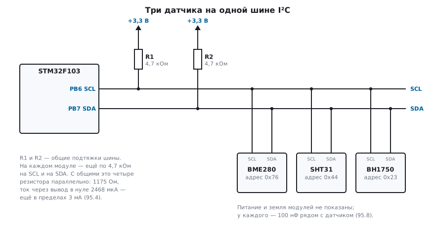
Each module brings its own pull-ups, and on the bus they are in parallel. How much current the pin has to sink at a low level with a 3.3 V supply:
| 4.7 kΩ resistors | Combined | Current through the pin at low level |
|---|---|---|
| 1 | 4700 Ω | 617 µA |
| 2 | 2350 Ω | 1234 µA |
| 3 | 1566 Ω | 1851 µA |
| 4 | 1175 Ω | 2468 µA |
| 5 | 940 Ω | 3085 µA |
Five such resistors push the current past the 3 mA limit: the pin no longer guarantees a low level below 0.4 V, and the receivers start to confuse zero with one. The cure is to keep the pull-ups on one module only (on the others this is usually a jumper or a pair of resistors you can desolder) and check the remaining one against 95.3.
95.5 Wire length
A wire is a capacitance too. Take as an example 70 pF per meter, and three sensors and the microcontroller pin at 10 pF each. Then a 4.7 kΩ pull-up at 100 kHz handles 3.01 m of wire, and 2.2 kΩ at 400 kHz only 1.71 m. Beyond that, either a lower speed, a stronger pull-up (within the limits of 95.3), or a bus buffer that splits the bus into segments, each with its own capacitance.
Besides capacitance, a wire picks up noise. Route SDA and SCL next to ground: in a flat ribbon cable, with a ground conductor in between; in twisted pair, each signal paired with its own ground.
95.6 MOSFET level shifter
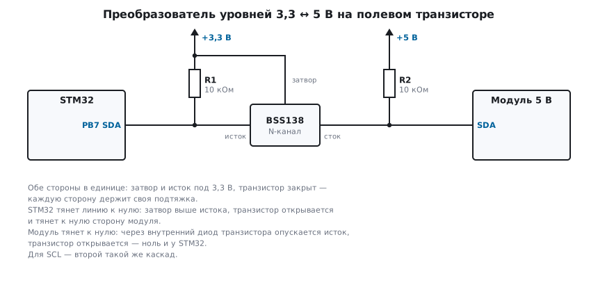
If a module pulls the bus up to 5 V and its pull-ups cannot be removed, you fit a bidirectional shifter built on an N-channel MOSFET, one per line. The gate goes to 3.3 V, the source to the microcontroller line, the drain to the module line, and each side has its own pull-up to its own supply:
- both sides high: gate and source are at the same voltage, the transistor is off, and each side is held by its own pull-up;
- the microcontroller pulls its side low: the gate ends up above the source, the transistor turns on and pulls the module side low;
- the module pulls its side low: the source goes down through the transistor's body diode, the transistor turns on, and the low level reaches the microcontroller.
Ready-made multi-line shifter boards are built exactly this way, usually with BSS138 transistors.
95.7 1-Wire, DHT and analog sensors
- 1-Wire is a single open-drain data line with a pull-up to the supply. In parasite power mode the sensor takes its energy from the line itself, and during a conversion the line is held high by a switch, not by a resistor.
- DHT11 and DHT22 also use one line, but with their own protocol: the pulse duration encodes the bit, and the pull-up determines how steeply the line returns to high.
- Analog sensor: the ADC input charges its sampling capacitor, and a high-impedance source does not get enough sampling time. The capacitor at the input and the sampling time are covered in sections 14 and 50.
95.8 Decoupling and ground
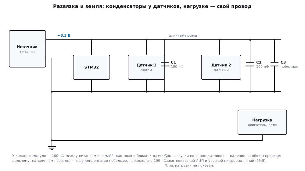
- Each module gets a 100 nF capacitor between supply and ground, as close to the sensor as possible. On ready-made modules it is usually already fitted; for a bare chip it is your job.
- The ground of the sensors and the microcontroller is one, and a high-current load (motor, relay, gas sensor heater) runs its own ground wire to the source, not through the sensor ground: the voltage drop on a shared wire shifts the readings of analog sensors and the levels of digital lines.
- A distant sensor on a long wire also gets a larger capacitor right at the sensor, in parallel with the 100 nF.
95.9 Pitfalls
The bus works with one module and stops with three. The module pull-ups add up: five at 4.7 kΩ already make 940 Ω and more than 3 mA through the pin. Keep the pull-ups on one module only.
The bus works on the bench and fails on a wire. The wire capacitance ate the edge margin: at 400 kHz with a 2.2 kΩ pull-up you get only 1.71 m. Lower the speed, recalculate the pull-up, fit a buffer.
The built-in pull-up is "enough" as long as the wires are short. Tens of kilohms give edges of microseconds, and the bus works one moment and not the next. For I²C use only external resistors.
A 5 V module pulls the bus up to five volts. An input that is not 5 V tolerant gets current through its protection diodes (section 62). Remove the module pull-ups or fit a level shifter.
A 5 V analog sensor output goes straight to the ADC input. No more than 3.3 V on an ADC input; you need a divider.
No common ground. The levels mean nothing, and the sensor "answers with garbage".
95.10 Summary
- A module is a sensor plus support parts: before connecting, find the pull-ups and work out which supply they go to.
- The best case is a 3.3 V sensor; a 5 V module needs a divider, an FT pin or a level shifter.
- The I²C edge rises in 0.8473·R·C and must fit into 1000 ns at 100 kHz and 300 ns at 400 kHz; the pull-up lies between (supply − 0.4 V) / 3 mA and t / (0.8473·C).
- Module pull-ups add up: five at 4.7 kΩ push the current past 3 mA.
- A wire is a capacitance: at 400 kHz with 2.2 kΩ, 1.71 m at 70 pF/m.
- A bidirectional shifter is one MOSFET per line, with the gate at 3.3 V.
- Each module gets 100 nF, the ground is one, and a high-current load has its own wire.
Next: section 95а "Level shifters: a transistor with pull-ups, TXB and TXS — why the module fails with I²C and a long wire" — ready-made TXB and TXS modules, why they do not get along with I²C pull-ups and long wires, and when an FT pin does the job without a shifter.