 Embedded HandbookApps
95а. Level shifters: a transistor with pull-ups, TXB and TXS — why the module fails with I²C and a long wire
Section 95.6 covers the MOSFET switch: gate at 3.3 V, one pull-up on each side, and the I²C line works in both directions without a direction pin. But on the module market there are fewer such switches than boards built on chips with "automatic" direction: the eight-channel TXB0108 and TXS0108E. They look the same from outside: eight lines, two supply pins, an OE pin. They behave differently, and this is exactly where the complaints come from: "the I²C sensor does not answer through the module" and "SPI works over half a meter of wire, over a meter it is garbage".
This section covers: three kinds of shifter and what each can do; the edges of the transistor switch with different pull-ups and capacitances; a model of a buffer with a weak output and edge accelerators, like the TXB, on the I²C bus and on a wire; the frequency each option reaches; when you do not need a shifter at all because the STM32 pin tolerates 5 V; a selection table for I²C, SPI, UART and 1-Wire.
Sources: DocID13587 Rev 17 (F103x8/xB pins and their FT marking, the voltage limit on an FT pin, the note about pull-ups), DS8626 Rev 9 (the same for the F407), RM0008 (DocID13902 Rev 17, F1 pin modes: pull-ups only in input mode). The I²C edge limits of 1000 and 300 ns and the thresholds of 0.3 and 0.7 of the supply come from 95.3 and section 17. The principle of the TXB and TXS follows the descriptions in the manufacturer's application notes (TI SCEA043, SCEA044, SCEA054), retold; the section has not been checked against their datasheets, so the manufacturer's numbers (output impedance, accelerator current, one-shot duration, allowed pull-up) are not given here. All the models are our own, in ngspice 39; their parameters are stated below and chosen to illustrate the mechanism, not taken from the chip datasheets.
What it is called in the documentation
Original Meaning level translator, level shifter a circuit that converts logic levels auto-direction sensing the chip detects the direction by itself edge-rate accelerator, one-shot a circuit that speeds up an edge; a pulse of fixed length pass transistor a transistor switch between the two sides body diode the diode built into the transistor open-drain / push-pull output that only pulls low / output that drives both levels direction control (DIR) the pin that sets the direction output enable (OE) the pin that enables the outputs five-volt tolerant (FT) a pin that tolerates 5 V
95а.1 Three devices under one name
Transistor switch. One N-channel MOSFET per line (most often a BSS138) and two pull-ups, to 3.3 V and to 5 V. The transistor itself never pulls anything high: it only passes a low level from one side to the other. The high level on each side is made by the pull-up, so the rising edge is the capacitance charging through a resistor, as on any open-drain bus (95.3).
Buffer with a weak output and accelerators (TXB). Inside there are two buffers facing opposite ways. Each drives its side to its own supply, but through a high output impedance: any external output overpowers it, and this is how the direction is detected. To keep the edge from being slow, on a level change a one-shot fires and for a short time connects strong switches to the line: to the supply on a rising edge, to ground on a falling edge. Such a buffer is designed for push-pull lines: SPI, UART, plain signals. An external pull-up fights the weak output, and a long wire fights the one-shot (95а.3, 95а.4).
Switch with pull-ups and accelerators (TXS). In principle it is the same transistor switch: a pass transistor between the sides, pull-ups already inside, and accelerators for the rising edge. So the TXS suits open-drain lines (I²C, 1-Wire), and its pull-ups add up with the external ones and the module's (95.4). There is no separate TXS model in this section: on I²C it behaves like the switch from 95а.2, only with a faster rising edge.
Push-pull buffer with a direction pin. An ordinary buffer with two supplies: the DIR pin sets the direction, and the output is strong both low and high. It detects nothing by itself, so it gets in the way of nothing; it does not suit I²C, because the line there is bidirectional and open-drain.
95а.2 Transistor switch: edges and levels
The model: our own model of a small N-channel transistor (threshold 1.3 V, a drain-source body diode, small capacitances); the microcontroller and sensor pins are 25 Ω open-drain switches. The microcontroller side is 3.3 V, the module side is 5 V, the pull-ups are equal on both sides, and so are the capacitances. First the microcontroller pulls the line low, then releases it; then the sensor does the same from its side. The edge of the opposite side is measured from 0.3 to 0.7 of its supply, as in the I²C standard.
.include fet.inc
.param rl=4.7k rh=4.7k ca=50p cb=50p vl=3.3
VL l 0 DC {vl}
VH h 0 DC 5
Rl l a {rl}
Rh h b {rh}
Ca a 0 {ca}
Cb b 0 {cb}
M1 b l a MSS
Sa a 0 ka 0 SWD
Sb b 0 kb 0 SWD
Vka ka 0 PULSE(0 1 2u 1n 1n 30u 1)
Vkb kb 0 PULSE(0 1 62u 1n 1n 30u 1)
.tran 1n 122u 0 2n
| Capacitance of each side | Pull-ups | Edge on the 5 V side | Edge on the 3.3 V side |
|---|---|---|---|
| 50 pF | 10 kΩ | 577 ns | 384 ns |
| 50 pF | 4.7 kΩ | 269 ns | 185 ns |
| 50 pF | 2.2 kΩ | 124 ns | 89 ns |
| 200 pF | 10 kΩ | 1973 ns | 1271 ns |
| 200 pF | 4.7 kΩ | 920 ns | 614 ns |
| 200 pF | 2.2 kΩ | 427 ns | 295 ns |
The 5 V side rises more slowly than a single RC: for 10 kΩ and 50 pF the formula from 95.3 gives 424 ns, and the model gives 577. As long as the 3.3 V side is not above the gate minus the threshold, the transistor is on, and the 5 V pull-up charges both capacitances at once; after that the 5 V side is pulled up alone. The 3.3 V side, on the contrary, rises faster than its own RC: at the start the 5 V pull-up helps it.
The low level passes well: on the opposite side from 0.02 to 0.10 V (more with a strong pull-up), the falling edge is from 5.6 to 19.0 ns. If the sensor pulls the 5 V side low, the transistor first opens through its own body diode, and then through the channel.
What this means for I²C. At 100 kHz (edge up to 1000 ns) with 50 pF any pull-up from the table will do, with 200 pF 4.7 and 2.2 kΩ. At 400 kHz (up to 300 ns) with 50 pF, 4.7 and 2.2 kΩ, and with 200 pF none will do: even with 2.2 kΩ the 5 V side rises in 427 ns. Calculate for the 5 V side: it is the slower one.
The same cell with a 1.8 V microcontroller (and the gate at 1.8 V): the low level on the 5 V side is 0.044 V, the edge is 234 ns at 4.7 kΩ and 50 pF. The model with a threshold of 1.3 V works here, but the "gate minus threshold" margin is only 0.5 V: look up the threshold of your transistor in its datasheet: if it is close to 1.8 V, the switch will turn on poorly or not at all.
95а.3 Buffer with accelerators on I²C: the pull-up fights the weak output
A model of one channel on the TXB principle, our own and simplified, with parameters for illustration: weak output 4 kΩ, accelerator a 30 Ω switch for about 10 ns, the threshold of each side half of its supply:
.subckt TXBCH a b va vb params: rw=4k racc=30 tos=14.4n
* логическое состояние стороны с задержкой входа 0,5 нс
Bsa sa0 0 V = 0.5*(1+tanh((V(a)-V(va)/2)/0.05))
Rsa sa0 sa 1k
Csa sa 0 0.5p
Bsb sb0 0 V = 0.5*(1+tanh((V(b)-V(vb)/2)/0.05))
Rsb sb0 sb 1k
Csb sb 0 0.5p
* встречные буферы со слабым выходом
Bdb nb 0 V = V(vb)*V(sa)
Rwb nb b {rw}
Bda na 0 V = V(va)*V(sb)
Rwa na a {rw}
* одновибраторы: сглаженная копия состояния отстаёт на tos; разница больше 0,5 — ускоритель включён
Efa fa0 0 sa 0 1
Rfa fa0 fa 1k
Cfa fa 0 {tos/1000}
Efb fb0 0 sb 0 1
Rfb fb0 fb 1k
Cfb fb 0 {tos/1000}
* фронт на любой стороне включает ускорители обеих сторон
Bup up 0 V = 0.5*(1+tanh((max(V(sa)-V(fa),V(sb)-V(fb))-0.5)/0.02))
Bdn dn 0 V = 0.5*(1+tanh((max(V(fa)-V(sa),V(fb)-V(sb))-0.5)/0.02))
Bua 0 a I = (V(va)-V(a))/{racc}*V(up)
Bda2 a 0 I = V(a)/{racc}*V(dn)
Bub 0 b I = (V(vb)-V(b))/{racc}*V(up)
Bdb2 b 0 I = V(b)/{racc}*V(dn)
Dpa a va DCL
Dna 0 a DCL
Dpb b vb DCL
Dnb 0 b DCL
.model DCL D(IS=1e-14 N=1 RS=2)
.ends
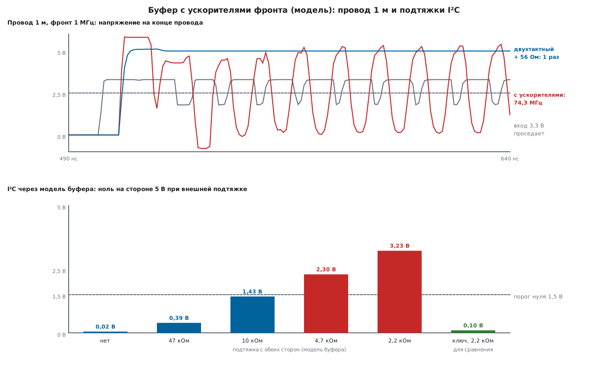
We put it on the I²C bus: an open-drain microcontroller on the 3.3 V side, external pull-ups of the same value on both sides (as on the sensor module and on the microcontroller board). The microcontroller pulls its side low; what does the sensor get:
| External pull-ups | Low level on the 5 V side | After the sensor pulled its side low: low level on the 3.3 V side | Line after release |
|---|---|---|---|
| none (1 MΩ) | 0.02 V | 0.01 V | stayed low |
| 47 kΩ | 0.39 V | 0.26 V | stayed low |
| 10 kΩ | 1.43 V | 0.94 V | stayed low |
| 4.7 kΩ | 2.30 V | 1.52 V | stayed low: 2.31 and 1.52 V |
| 2.2 kΩ | 3.23 V | 2.13 V | returned: 5.00 and 3.30 V |
The mechanism is simple: the one-shot pulls the line down only for the duration of its pulse, and after that the low level is held by the weak output against the external pull-up, which makes a divider. With a weak pull-up the low level is clean; with 10 kΩ it is already at the edge of the thresholds (1.5 V for the 5 V side and 0.99 V for 3.3 V, i.e. 0.3 of the supply); with 4.7 kΩ it is no lower than 2.30 V; with 2.2 kΩ there is no low level at all: 3.23 V is a high for the sensor.
The last column is worse. An open-drain output does not make a high level by itself: it only releases the line. But the buffer remembers the low level and holds it with its weak output on both sides. Only a pull-up can return the line high, one that pulls the divider over the buffer threshold; in the model this worked only with 2.2 kΩ, when there is no low level anymore. With all the other pull-ups the bus hung after the very first low level. A window where both low and high work does not exist for such a buffer on an open-drain line.
The numbers depend on the model parameters, the conclusion does not: a buffer with a weak output is designed for push-pull outputs, which make both low and high by themselves. I²C sensor modules bring their own pull-ups (95.4), and that is why a TXB is not used on I²C.
95а.4 Buffer with accelerators on a wire
Now the 5 V side goes over a wire to a receiver. The wire is a lossless line with 70 pF and 0.5 µH per meter: 84.5 Ω and 5.92 ns per meter. At the end there is a 10 pF input with diodes to supply and ground. The microcontroller drives a 1 MHz square wave from a push-pull output, two periods, i.e. four edges. We count how many times the receiver crossed 2.5 V:
| Wire | Buffer model with accelerators | Push-pull buffer | Push-pull + 56 Ω |
|---|---|---|---|
| 0.25 m | 4 transitions | 4 | 4 |
| 1 m | 296 | 4 | 4 |
| 2 m | 159 | 4 | 4 |
At 0.25 m all three are clean. At one meter the buffer model with accelerators breaks into oscillation: the accelerator throws an edge into the wire, the reflection comes back after twice the delay and pushes the side over the threshold; the one-shot now fires in the opposite direction, and so on without end. From 0.6 to 0.95 µs, when the input has long been high, the receiver switched 52 times, i.e. 74.3 MHz; at 2 m, 28 times, 40.0 MHz. The accelerator on the 3.3 V side meanwhile fights the microcontroller output: the buffer input itself sags to 1.76 V (to 1.77 V at 2 m).
The push-pull buffer gives no false transitions, but it rings: overshoot up to 5.93 V and undershoot down to −0.93 V, and only the input diodes clip them. A series termination resistor of 56 Ω (together with the 25 Ω output this is close to the characteristic impedance of the wire, section 160) removes the ringing: at one and two meters the maximum is 5.12 V and the minimum is no lower than −0.12 V; at 0.25 m, 5.05 and −0.05 V.
How long a wire a real TXB can handle, the model cannot tell: that depends on its accelerators. It tells something else: an automatic buffer with accelerators is a loop with positive feedback through the wire, and on a long line it can break into oscillation. A push-pull buffer with a direction pin has no such loop.
95а.5 Speed
A square wave from the microcontroller's push-pull output (3.3 V) passes to the 5 V side with a 50 pF load: the module input and a short wire. We count how many of the 16 edges (eight periods) arrive completely, below 1.5 and above 3.5 V:
| Frequency | Switch, 10 kΩ | Switch, 2.2 kΩ | Model with accelerators | Push-pull |
|---|---|---|---|---|
| 100 kHz | 16 | 16 | 16 | 16 |
| 400 kHz | 16 | 16 | 16 | 16 |
| 1 MHz | 16 | 16 | 16 | 16 |
| 2 MHz | 0 | 16 | 16 | 16 |
| 4 MHz | 0 | 16 | 16 | 16 |
| 10 MHz | 0 | 0 | 16 | 16 |
| 20 MHz | 0 | 0 | 16 | 16 |
| 40 MHz | 0 | 0 | 14 | 16 |
The switch with 10 kΩ on the 5 V side works up to 1 MHz, with 2.2 kΩ up to 4 MHz: the rising edge here is always the capacitance charging through the pull-up. For SPI at several megahertz the switch does not suit. The limit of the model with accelerators depends on its parameters; the push-pull buffer (25 Ω output in the model) passed the whole list.
95а.6 Without a shifter: 5 V tolerant pins
The most reliable shifter is the one that is not there. A pin marked FT tolerates up to VDD + 4 V at its input (DocID13587 and DS8626, absolute maximum ratings table), with the supply applied and the built-in pull-ups turned off (general notes in 8.1). This gives two techniques:
- a 5 V signal coming in (MISO, RX from a five-volt module): straight to an FT pin, with no divider and no chip;
- an open-drain line to 5 V (I²C, 1-Wire, any signal going out): an FT pin in open-drain mode with the pull-up straight to 5 V. A 5 V module will see a full 5 V for a high level, and the edge is calculated as in 95.3.
Bus pins from the datasheets:
| Pins | Bus | F103 | F407 |
|---|---|---|---|
| PB6, PB7 | I2C1 | FT | FT |
| PB8, PB9 | I2C1 after remapping | FT | FT |
| PB10, PB11 | I2C2 | FT | FT |
| PA9, PA10 | USART1 | FT | FT |
| PA2, PA3 | USART2 | no | FT |
| PA5, PA6, PA7 | SPI1 | no | PA5 only 3.3 V (TTa), PA6, PA7 FT |
| PB13, PB14, PB15 | SPI2 | FT | FT |
On the F103, pins routed to the ADC do not tolerate 5 V: SPI1 and USART2 to a five-volt module only through a shifter, while SPI2 and USART1 go directly. On the F407, the SCK of the first SPI on PA5 is not tolerant; SPI1 on PB3–PB5 works without a shifter.
Your own open-drain pin to 5 V, for example PB8 in both families:
#if defined(STM32F10X_MD)
/* F103: MODE = 10 (выход, 2 МГц), CNF = 01 (открытый сток). Подтяжки у F1 включаются только в режиме входа. */
void od5v_pin(GPIO_TypeDef *port, uint32_t pin)
{
    volatile uint32_t *cr = (pin < 8u) ? &port->CRL : &port->CRH;
    uint32_t sh = (pin & 7u) * 4u;
    *cr = (*cr & ~(0xFu << sh)) | (0x6u << sh);
}
_Static_assert((GPIO_CRL_MODE0_1 | GPIO_CRL_CNF0_0) == 0x6u, "F103: MODE=10, CNF=01");
_Static_assert((GPIO_CRL_MODE0 | GPIO_CRL_CNF0) == 0xFu, "F103: четыре бита на вывод");
#else
/* F407: выход, открытый сток, низкая скорость, встроенные подтяжки выключены —
 * с ними вывод FT не держит напряжение выше VDD + 0,3 В. */
void od5v_pin(GPIO_TypeDef *port, uint32_t pin)
{
    port->MODER   = (port->MODER & ~(3u << (pin * 2u))) | (1u << (pin * 2u));
    port->OTYPER |= 1u << pin;
    port->OSPEEDR &= ~(3u << (pin * 2u));
    port->PUPDR  &= ~(3u << (pin * 2u));
}
_Static_assert(GPIO_MODER_MODER0_0 == 1u && GPIO_OTYPER_OT_0 == 1u && GPIO_PUPDR_PUPDR0 == 3u
               && GPIO_OSPEEDER_OSPEEDR0 == 3u, "F407: поля MODER, OTYPER, OSPEEDR, PUPDR");
#endif

/* Отпустить линию: единицу до 5 В даст внешняя подтяжка. */
void od5v_release(GPIO_TypeDef *port, uint32_t pin)
{
    port->BSRR = 1u << pin;
}

/* Прижать линию к нулю. */
void od5v_low(GPIO_TypeDef *port, uint32_t pin)
{
    port->BSRR = 1u << (pin + 16u);
}

/* Прочитать линию: вход читается и в режиме выхода с открытым стоком. */
uint32_t od5v_read(GPIO_TypeDef *port, uint32_t pin)
{
    return (port->IDR >> pin) & 1u;
}
The F1 has no separate pull-up register: according to RM0008 the pull-ups are connected only
in input mode, so open-drain is already "without pull-ups". On the F407 you have to
turn them off explicitly in PUPDR. For the I²C bus, the same pins in
alternate function mode are configured with the code from 95.3. The code builds for the
F103 and F407 without warnings: 64 and 86 bytes.
What FT does not solve: a 3.3 V output in push-pull mode gives too little to a five-volt input with a 3.5 V threshold (62.5). For a fast signal going out, use a push-pull buffer; for a slow one, open-drain with a pull-up to 5 V.
What to use:
| Line | What to use | What to avoid |
|---|---|---|
| I²C | an FT pin with pull-ups to 5 V; otherwise a transistor switch or TXS, edge as in 95а.2 | a buffer with a weak output (TXB): the module pull-ups overpower it |
| SPI | a push-pull buffer with DIR, one channel per line (MISO through a reverse channel or straight to FT); on a wire 33…56 Ω in series | a transistor switch above 1–4 MHz; a buffer with accelerators on a long wire |
| UART | RX from 5 V straight to FT; TX going out through a push-pull buffer or into a 5 V input with TTL thresholds (62.5) | pull-ups on the line with a weak-output buffer |
| 1-Wire | an FT pin with a pull-up to 5 V; otherwise a transistor switch | a buffer with a weak output: 1-Wire requires a pull-up |
95а.7 Pitfalls
The I²C sensor does not answer through an eight-channel module, and on the oscilloscope the low level hangs at about half the supply. The module has a buffer with a weak output (TXB), and the I²C outputs are open-drain. In the model with 4.7 kΩ pull-ups the low level does not drop below 2.30 V, and after release the line stays low. You need a transistor switch, a TXS or an FT pin.
With a TXS module the bus works, but the pin does not hold the low level. The built-in pull-ups of the TXS are in parallel with the pull-ups of the sensor module and the microcontroller board: the low-level current adds up, as in 95.4. Remove the extra pull-ups.
SPI through the module works on a breadboard, but on a one-meter wire it is garbage. A buffer with accelerators on a long line breaks into oscillation: in the model, at one meter the receiver switches 296 times instead of four. Use a push-pull buffer with a direction pin and a 33…56 Ω resistor at the output.
The transistor switch "cannot keep up" with SPI. The rising edge is the capacitance charging through the pull-up: with 10 kΩ and 50 pF up to 1 MHz, with 2.2 kΩ up to 4 MHz. The switch is not meant for fast push-pull lines.
The I²C edge was calculated by the formula, and there are still failures at 400 kHz. Through the switch the 5 V side rises more slowly than a single RC: 577 ns against 424 at 10 kΩ and 50 pF. Measure and calculate on the 5 V side.
The transistor switch does not work for 1.8 V. The gate is at 1.8 V, and the transistor threshold in the datasheet is close to that voltage: the channel turns on poorly or not at all. Use a transistor with a low threshold, or an FT pin.
A TXB/TXS module with the OE pin left floating. OE disables all the outputs; a floating input gives a random state. Tie OE to the supply of the side the datasheet assigns it to, or to a microcontroller pin.
A pull-up to 5 V on a pin without FT. PA5–PA7 on the F103 and PA5 on the F407 do not tolerate 5 V. Check the pin against the datasheet table, not against "the neighbor that worked".
95а.8 Summary
- Three devices: the transistor switch (open-drain), the buffer with a weak output and accelerators (TXB, push-pull lines), the switch with pull-ups and accelerators (TXS, open-drain); plus the push-pull buffer with DIR.
- The switch: low level 0.02–0.10 V, falling edge 5.6–19.0 ns; rising edge on the 5 V side 577 ns at 10 kΩ and 50 pF, 427 ns at 2.2 kΩ and 200 pF: 400 kHz at 200 pF does not pass.
- The weak-output buffer model on I²C: the low level on the 5 V side is 0.39 V at 47 kΩ, 1.43 V at 10 kΩ, 2.30 V at 4.7 kΩ, 3.23 V at 2.2 kΩ; after release the line returned high only with 2.2 kΩ.
- On a 1 m wire the model with accelerators oscillates at 74.3 MHz (296 transitions instead of 4), at 2 m at 40.0 MHz; the push-pull buffer gives 4 transitions, and with 56 Ω the overshoot is no higher than 5.12 V.
- Frequency at 50 pF: the switch with 10 kΩ up to 1 MHz, with 2.2 kΩ up to 4 MHz; the push-pull buffer the whole list up to 40 MHz.
- FT pins tolerate VDD + 4 V: I2C1, I2C2, USART1, SPI2 on the F103 and F407 need no shifter; SPI1 and USART2 on the F103 do.
Full source code
lvl95a.c: an open-drain line pulled up to 5 V on an FT pin.
/* Раздел 95а: линия с открытым стоком, подтянутая снаружи к 5 В, — без преобразователя уровней.
 * Только для выводов FT (терпимых к 5 В), например PB8 у F103 и F407. Собирается для F103 (-DSTM32F10X_MD,
 * stm32f10x.h) и для F407 (-DSTM32F407xx, stm32f4xx.h). */
#include <stdint.h>

#if defined(STM32F10X_MD)
/* F103: MODE = 10 (выход, 2 МГц), CNF = 01 (открытый сток). Подтяжки у F1 включаются только в режиме входа. */
void od5v_pin(GPIO_TypeDef *port, uint32_t pin)
{
    volatile uint32_t *cr = (pin < 8u) ? &port->CRL : &port->CRH;
    uint32_t sh = (pin & 7u) * 4u;
    *cr = (*cr & ~(0xFu << sh)) | (0x6u << sh);
}
_Static_assert((GPIO_CRL_MODE0_1 | GPIO_CRL_CNF0_0) == 0x6u, "F103: MODE=10, CNF=01");
_Static_assert((GPIO_CRL_MODE0 | GPIO_CRL_CNF0) == 0xFu, "F103: четыре бита на вывод");
#else
/* F407: выход, открытый сток, низкая скорость, встроенные подтяжки выключены —
 * с ними вывод FT не держит напряжение выше VDD + 0,3 В. */
void od5v_pin(GPIO_TypeDef *port, uint32_t pin)
{
    port->MODER   = (port->MODER & ~(3u << (pin * 2u))) | (1u << (pin * 2u));
    port->OTYPER |= 1u << pin;
    port->OSPEEDR &= ~(3u << (pin * 2u));
    port->PUPDR  &= ~(3u << (pin * 2u));
}
_Static_assert(GPIO_MODER_MODER0_0 == 1u && GPIO_OTYPER_OT_0 == 1u && GPIO_PUPDR_PUPDR0 == 3u
               && GPIO_OSPEEDER_OSPEEDR0 == 3u, "F407: поля MODER, OTYPER, OSPEEDR, PUPDR");
#endif

/* Отпустить линию: единицу до 5 В даст внешняя подтяжка. */
void od5v_release(GPIO_TypeDef *port, uint32_t pin)
{
    port->BSRR = 1u << pin;
}

/* Прижать линию к нулю. */
void od5v_low(GPIO_TypeDef *port, uint32_t pin)
{
    port->BSRR = 1u << (pin + 16u);
}

/* Прочитать линию: вход читается и в режиме выхода с открытым стоком. */
uint32_t od5v_read(GPIO_TypeDef *port, uint32_t pin)
{
    return (port->IDR >> pin) & 1u;
}
Next: section 96 "Temperature: NTC thermistor and DS18B20" — the first sensor of the part: an analog and a digital way to measure the same thing.