 Embedded HandbookApps
22в. Segment LCD: the glass, multiplexing and the LCD controller
In section 22 digits were shown by an LED display: a segment is lit while current flows through it, and the digits are lit in turn. Liquid crystal glass works differently — it does not emit light but changes its transparency with voltage, and draws almost no current. That is why clocks, meters and thermometers running on a battery use an LCD. Here — why the glass must not be fed a DC voltage, how hundreds of segments are driven through four common pins, how the built-in LCD controller of the L0, L1 and L4 series does it and how much it draws in Stop mode.
Prerequisites: reference manual RM0367 Rev 8 (STM32L0x3, chapter 17 "Liquid crystal display controller") and datasheet DS10152 Rev 9 for the STM32L053 — both from the Keil pack; the CMSIS headers of the L053, L152 and L476 from the packs. The voltage waveforms and rms values were computed with our own PC model by the rules of RM0367; the code was built with armclang for three chips.
Terms used in the documentation
Term Meaning liquid crystal display, LCD a display that changes transparency with voltage glass the display itself, without a controller common, COM a common electrode pin segment, SEG a segment electrode pin duty ratio, 1/4 duty multiplexing, 1/4 means four common pins bias, 1/3 bias the number of voltage levels: 1/3 means levels 0, 1/3, 2/3, 1 frame, frame rate one full drive cycle and how often it repeats step-up converter a converter that raises the voltage contrast control adjusting the drive voltage double buffer a written copy and a displayed copy of the data
22в.1 Why not direct current
A segment is a layer of liquid crystal between two transparent electrodes. When the voltage across the layer is above a threshold, the molecules turn and the segment darkens. But a DC voltage damages the glass: RM0367 explicitly requires alternating the polarity, otherwise electrophoresis begins — the crystal degrades. So each segment must have an AC voltage with an average of exactly zero.
The simplest way is static drive: the glass has one common COM pin for all segments, and each segment has its own SEG pin. A square wave 0 / VLCD goes to COM. If a segment must be on, the same square wave in antiphase is applied to its SEG: across the layer there is ±VLCD, rms VLCD. If it must be off — in phase: zero across the layer. The contrast is at maximum, but as many pins are needed as there are segments: on the L053 up to 51 in static mode.
Fortunately the darkness depends not on the instantaneous but on the rms voltage: the glass is slow. This is what opens the way to multiplexing.
22в.2 Multiplexing: duty and bias
Take four common pins COM0…COM3 (1/4 duty). Each SEG pin now goes to four segments — one for each COM. The frame is divided into four phases; in phase n COMn is "active", and the segments of this COM are turned on or off by the level on SEG. So that the segments of the other COMs do not light up at this time, the excess voltage is suppressed with intermediate levels — this is the bias. With 1/3 bias according to RM0367:
- the active COM in an odd frame is VLCD, in an even frame 0; an inactive one is 1/3 and 2/3 VLCD;
- the SEG of a lit segment is the opposite rail (0 in the odd frame, VLCD in the even one); the SEG of an unlit one is 2/3 and 1/3 VLCD.
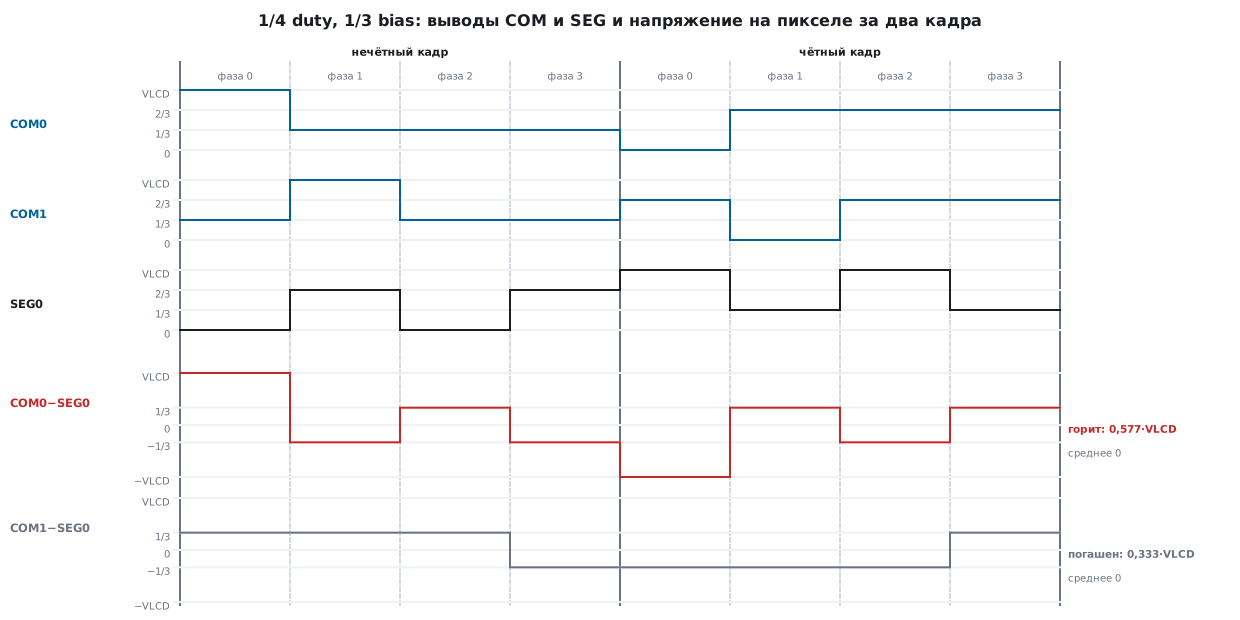
The model builds these waveforms for each pixel and tries all combinations of neighbouring pixels on the same SEG. The result does not depend on the neighbours, and the average over a pair of frames is exactly zero (over one frame it is not, up to 0.5 VLCD: that is why frames come in pairs). The "on / off" ratio is the main measure of contrast:
| Multiplexing | Bias | On, fraction of VLCD | Off | Ratio |
|---|---|---|---|---|
| static | — | 1 | 0 | infinity |
| 1/2 | 1/2 | 0.7906 | 0.3536 | 2.236 |
| 1/3 | 1/3 | 0.6383 | 0.3333 | 1.915 |
| 1/4 | 1/3 | 0.5774 | 0.3333 | 1.732 |
| 1/4 | 1/2 | 0.6614 | 0.4330 | 1.528 |
| 1/4 | 1/4 | 0.5449 | 0.3307 | 1.648 |
| 1/8 | 1/4 | 0.4239 | 0.2932 | 1.446 |
The model agrees with the classic formula (1/a)·√((a² + N − 1)/N) for
a lit segment and (1/a)·√(((a − 2)² + N − 1)/N) for an unlit one (N is the number of COMs,
a is the bias denominator). Two things are visible. The more COMs, the worse the distinction —
so 1/8 duty is suitable only for glass with a sharp threshold. And the bias
is matched to the multiplexing: with four COMs 1/3 gives 1.732, while 1/2 and 1/4 give
less. What multiplexing and bias are needed is stated in the glass datasheet.
The absolute numbers depend on VLCD. On the L053 the internal step-up converter delivers from 2.6 to 3.55 V (eight CC steps, DS10152); at step VLCD3 = 2.98 V with 1/4 duty and 1/3 bias a lit segment gets 1.721 V, an unlit one 0.993 V. The threshold of the glass must lie between them — it is taken from the glass datasheet and matched with the CC step.
22в.3 The LCD controller: where it exists and how it is built
A built-in controller exists on the L0 (L053, L063, L073 etc.), L1, L4 (L476 and neighbours) and U0 (RM0503, chapter 19); the U5 does not have it — there is no such block in the table of contents of RM0456. On the L0, L1 and L4 it sits at the same address 0x4000 2400 and has identical fields — one and the same code builds for all three:
| Register | Offset | What it holds |
|---|---|---|
| LCD_CR | 0x00 | DUTY (bits 4:2), BIAS (6:5), VSEL (1), LCDEN (0), MUX_SEG (7) |
| LCD_FCR | 0x04 | PS (25:22), DIV (21:18), BLINK, BLINKF, CC (12:10), DEAD, PON (6:4), HD |
| LCD_SR | 0x08 | FCRSF (5), RDY (4), UDD (3), UDR (2), SOF (1), ENS (0) |
| LCD_CLR | 0x0C | clearing the UDD and SOF flags |
| LCD_RAM | 0x14…0x50 | 16 words: for COMn word 2n (SEG0…31) and 2n+1 (SEG32…51) |
Field codes per RM0367: DUTY 000 — static, 001 — 1/2, 010 — 1/3, 011 — 1/4, 100 — 1/8; BIAS 00 — 1/4, 01 — 1/2, 10 — 1/3. The controller drives up to 8 COMs and up to 52 SEGs. The memory is double: the program writes LCD_RAM, sets UDR, and at the start of the next frame the data goes to the display buffer; while UDR is set, LCD_RAM is closed to writes. The COM and SEG pins are configured as an alternate function.
22в.4 Frame rate
The LCDCLK clock is the same as for the real-time clock: LSE, LSI or HSE with a divider. Then two dividers from LCD_FCR:
f_ck_div = f_LCDCLK / (2^PS · (16 + DIV))
f_кадр   = f_ck_div · duty
The check recomputed all 15 rows of table 74 of RM0367 with this formula —
they agree to the hundredth: for example, from an LSE of 32 768 Hz with PS = 4, DIV = 1 and 1/4
duty the result is 30.12 Hz. The RM advises keeping the frame between roughly 30 and 100 Hz:
below that — flicker, above — wasted current. Take PS = 3, DIV = 1: ck_div =
240.94 Hz, the frame at 1/4 duty is 60.24 Hz.
Blinking is clocked from the same ck_div frequency: f_ck_div / 2^(BLINKF + 3),
with BLINKF = 5 it is 0.941 Hz. The PON pulse length (how long to keep the
low-impedance divider on after a level change) is counted in ck_ps cycles: with
PS = 3 one cycle is 244.1 µs.
22в.5 The font and the segment table
The font is the same as in section 22: bit 0 is segment a, bit 6 is g, bit 7 is the dot. What is new is the glass table: which segment sits at the crossing of which COM and which SEG. It is different for each glass and is taken from its datasheet. As an example — a hypothetical four-digit glass with two SEG pins per digit:
| Pin 0 of the digit | Pin 1 of the digit | |
|---|---|---|
| COM0 | f | a |
| COM1 | g | b |
| COM2 | e | c |
| COM3 | d | dot |
void lcd_encode(uint32_t ram[16], const uint8_t pat[4])
{
    for (int i = 0; i < 16; i++)
        ram[i] = 0;
    for (int d = 0; d < 4; d++)
        for (int com = 0; com < 4; com++)
            for (int k = 0; k < 2; k++)
                if (pat[d] >> GLASS[com][k] & 1u) {
                    unsigned seg = PIN[d][k];
                    ram[2 * com + seg / 32] |= 1UL << (seg % 32);
                }
}
GLASS is the table above, PIN is which SEG pins are routed to a digit.
Changing the glass or the routing changes only these two tables. A PC model
decodes the LCD_RAM image back into digits: all 10 000 numbers with a dot in
any of the four positions and without it come back without errors, and a gcc build
of the same file gives on the PC the same 50 000 images as the model. The number 12.34
(dot after the second digit) is the words 00000068 00000000 000000FE 00000000
000000A6 00000000 0000001C 00000000.
22в.6 Start-up and output
void lcd_init(void)
{
    LCD->FCR = (3UL << LCD_FCR_PS_Pos) | (1UL << LCD_FCR_DIV_Pos) | (3UL << LCD_FCR_CC_Pos) | (2UL << LCD_FCR_PON_Pos);
    while (!(LCD->SR & LCD_SR_FCRSR)) {}            /* флаг FCRSF по RM: FCR перешёл в домен LCDCLK */
    LCD->CR = (2UL << LCD_CR_BIAS_Pos) | (3UL << LCD_CR_DUTY_Pos);   /* BIAS 10 = 1/3, DUTY 011 = 1/4, VSEL 0 */
    LCD->CR |= LCD_CR_LCDEN;
    while (!(LCD->SR & LCD_SR_ENS)) {}
    while (!(LCD->SR & LCD_SR_RDY)) {}              /* повышающий преобразователь вышел на напряжение */
}
The order is as in the HAL from the pack: first LCD_FCR and waiting for synchronisation, then
LCD_CR, enabling, waiting for ENS and RDY. The DUTY, BIAS, VSEL and MUX_SEG fields are
write-protected after enabling — they are chosen before LCDEN. armclang builds
this file for the L053, L152 and L476 without warnings; _Static_assert
checks against the headers of each chip the address 0x4000 2400, LCD_RAM from 0x14
for 16 words and the positions of all fields. The disassembly confirms the constants:
LCD_FCR = 0x00C4 0C20, LCD_CR = 0x4C. Together with the encoding it is 360 bytes of code
on the L053 and 414 on the L152 and L476.
Displaying a number: wait until UDR clears, write words 0…7 (for 1/4 duty only COM0…COM3 are needed) and set UDR — the transfer happens at the start of the next frame, without flicker and without interrupts.
Current in Stop. The controller works in Stop (not in Standby). According to table 39 of DS10152 it adds in Stop at 25 °C 0.15 µA in static mode and 1.6 µA (1.8 V) or 2.6 µA (3.0 V) at 1/8 duty. The current of the controller itself with the internal step-up converter per table 79 is 3.1 µA at 3.0 V (1/8 duty, 1/4 bias, no glass). For comparison, the whole chip in Stop with the RTC draws 0.8 µA. The divider itself on high-value resistors (6.6 MΩ) conducts 0.452 µA at 2.98 V; the current for recharging the glass capacitance depends on the glass and is not given in the datasheet — it is measured on your own board.
22в.7 Pitfalls
The glass fades or "sticks" after months. A DC component: a COM or SEG pin is toggled by software without alternating frames or switched off in the middle of a frame. After LCDEN is cleared the controller itself finishes the even frame and only then switches off the divider — do not bypass it by toggling pins in software.
All segments are half grey. The wrong bias or multiplexing for the glass, or VLCD is too high: an unlit segment at 1/4 duty gets 0.577 of a lit one, and the threshold of the glass must lie between them. Lower CC or enable the DEAD pause.
The FCRSF flag cannot be found. In RM0367 it is FCRSF, while in the CMSIS headers of the L0, L1
and L4 it is LCD_SR_FCRSR. And it must be waited for after writing LCD_FCR: reading
LCD_FCR returns the last value written, not the one the current frame is running with.
New digits did not appear. A write to LCD_RAM while UDR = 1 is ignored, and the transfer does not happen at all while LCDEN = 0. Only the hardware clears UDR.
LCD_CR does not change. After enabling, the DUTY, BIAS, VSEL and MUX_SEG fields are protected. First LCDEN = 0 and wait for ENS = 0.
The contrast "per the RM" did not match the datasheet. RM0367 gives the CC range as 2.60…3.51 V, while DS10152 for the L053 gives VLCD7 = 3.55 V. Take numbers only from the datasheet of your chip. And in the PON table of RM0367 the value for 011 is 782 µs, although three cycles of 244.1 µs are 732.4 µs.
The UDD interrupt is silent in Stop. RM0367: in Stop there are no bus clocks, and UDD gives no interrupt even with UDDIE = 1. For sleep, update LCD_RAM before entering Stop.
The VLCD pin is floating. With the internal converter VLCD needs a capacitor to ground (on the L053 from 0.1 to 2 µF); without an LCD the pin is connected to VDDA.
22в.8 Summary
- The average voltage on a segment is exactly zero over a pair of frames; otherwise the glass degrades.
- Static: 1 and 0 VLCD; 1/4 duty with 1/3 bias: 0.577 and 0.333 VLCD, a ratio of 1.732 — the best for four COMs; 1/8 duty with 1/4 bias only 1.446.
- L053: VLCD from 2.6 to 3.55 V; at 2.98 V a lit segment gets 1.721 V and an unlit one 0.993 V.
- The LCD controller: L0, L1, L4, U0 (not on the U5); address 0x4000 2400, 16 words of LCD_RAM, double buffering through UDR.
- Frame
LCDCLK / (2^PS · (16 + DIV)) · duty: from LSE with PS = 3, DIV = 1, 1/4 duty it is 60.24 Hz; table 74 of RM0367 agrees in all 15 rows. - In Stop the controller adds 0.15 µA (static) … 2.6 µA (1/8 duty, 3 V); with the step-up converter its current per the datasheet is 3.1 µA.
- The code for three chips is 360…414 bytes, the font and the glass are two tables.
Full sources
seglcd22d.c — four digits on a segment LCD through the LCD controller.
/* seglcd22d.c — раздел 22в: четыре цифры на сегментном ЖКИ через контроллер LCD.
 *
 * Стекло условное: 4 разряда, 1/4 duty, на разряд два вывода SEG (у настоящего стекла таблица — из его паспорта).
 * Кодирование (lcd_digits, lcd_encode) — чистые функции: их гоняет и gcc на ПК, и armclang для кристалла.
 * Работа с регистрами — только когда задан кристалл (-DSTM32L053xx, -DSTM32L152xB, -DSTM32L476xx):
 * у всех трёх LCD по адресу 0x4000 2400 и одинаковые поля CR, FCR, SR (RM0367 гл. 17, RM0038, RM0351).
 */
#include <stddef.h>
#include <stdint.h>

/* Шрифт как в разделе 22: бит 0 — сегмент a, …, бит 6 — g, бит 7 — точка. */
static const uint8_t FONT[10] = { 0x3F, 0x06, 0x5B, 0x4F, 0x66, 0x6D, 0x7D, 0x07, 0x7F, 0x6F };

/* GLASS[com][k] — какой сегмент разряда зажигает пара (COMcom, k-й вывод разряда). */
static const uint8_t GLASS[4][2] = {
    { 5, 0 },   /* COM0: f, a */
    { 6, 1 },   /* COM1: g, b */
    { 4, 2 },   /* COM2: e, c */
    { 3, 7 },   /* COM3: d, точка */
};
/* PIN[d][k] — номер вывода SEG у k-го вывода разряда d (как разведена плата). */
static const uint8_t PIN[4][2] = { { 0, 1 }, { 2, 3 }, { 4, 5 }, { 6, 7 } };

/* Число 0…9999 в сегменты; ведущие нули гасятся; dp — разряд с точкой (0…3) или −1. */
void lcd_digits(uint8_t pat[4], unsigned v, int dp)
{
    for (int d = 3; d >= 0; d--) {
        pat[d] = (v != 0 || d == 3) ? FONT[v % 10] : 0;
        v /= 10;
    }
    if (dp >= 0 && dp < 4)
        pat[dp] |= 0x80;
}

/* Сегменты в образ LCD_RAM: для COMn — слова 2n (SEG0…31) и 2n+1 (SEG32…51). */
void lcd_encode(uint32_t ram[16], const uint8_t pat[4])
{
    for (int i = 0; i < 16; i++)
        ram[i] = 0;
    for (int d = 0; d < 4; d++)
        for (int com = 0; com < 4; com++)
            for (int k = 0; k < 2; k++)
                if (pat[d] >> GLASS[com][k] & 1u) {
                    unsigned seg = PIN[d][k];
                    ram[2 * com + seg / 32] |= 1UL << (seg % 32);
                }
}

#if defined(LCD_BASE)
_Static_assert(LCD_BASE == 0x40002400UL, "LCD на APB1: 0x4000 2400");
_Static_assert(offsetof(LCD_TypeDef, RAM) == 0x14 && sizeof(((LCD_TypeDef *)0)->RAM) == 16 * 4, "LCD_RAM: 16 слов с 0x14");
_Static_assert(LCD_CR_DUTY_Pos == 2 && LCD_CR_BIAS_Pos == 5, "DUTY 4:2, BIAS 6:5");
_Static_assert(LCD_FCR_PS_Pos == 22 && LCD_FCR_DIV_Pos == 18 && LCD_FCR_CC_Pos == 10 && LCD_FCR_PON_Pos == 4, "PS, DIV, CC, PON");
_Static_assert(LCD_SR_FCRSR == 0x20 && LCD_SR_RDY == 0x10 && LCD_SR_UDR == 0x04 && LCD_SR_ENS == 0x01, "FCRSF (в заголовке FCRSR), RDY, UDR, ENS");

/* LCDCLK = LSE 32 768 Гц (выбор источника в RCC и выводы как альтернативная функция — раздел 12, здесь нет).
 * Кадр: 32768 / (2^3 · (16 + 1)) / 4 = 60,24 Гц; 1/4 duty, 1/3 bias, внутренний повышающий преобразователь. */
void lcd_init(void)
{
    LCD->FCR = (3UL << LCD_FCR_PS_Pos) | (1UL << LCD_FCR_DIV_Pos) | (3UL << LCD_FCR_CC_Pos) | (2UL << LCD_FCR_PON_Pos);
    while (!(LCD->SR & LCD_SR_FCRSR)) {}            /* флаг FCRSF по RM: FCR перешёл в домен LCDCLK */
    LCD->CR = (2UL << LCD_CR_BIAS_Pos) | (3UL << LCD_CR_DUTY_Pos);   /* BIAS 10 = 1/3, DUTY 011 = 1/4, VSEL 0 */
    LCD->CR |= LCD_CR_LCDEN;
    while (!(LCD->SR & LCD_SR_ENS)) {}
    while (!(LCD->SR & LCD_SR_RDY)) {}              /* повышающий преобразователь вышел на напряжение */
}

void lcd_show(unsigned v, int dp)
{
    uint8_t pat[4];
    uint32_t ram[16];
    lcd_digits(pat, v, dp);
    lcd_encode(ram, pat);
    while (LCD->SR & LCD_SR_UDR) {}                 /* пока идёт перенос, LCD_RAM закрыта для записи */
    for (int i = 0; i < 8; i++)                     /* 1/4 duty: COM0…COM3 — слова 0…7 */
        LCD->RAM[i] = ram[i];
    LCD->SR = LCD_SR_UDR;                           /* перенос в буфер показа в начале следующего кадра */
}
#endif
Next: section 22г "Addressable LEDs: WS2812B, SK6812 RGBW and SK6812WWA — protocol, timing, SPI, timer with DMA, power and levels".