 Embedded HandbookApps
22б. A camera over DCMI: a frame into memory through DMA
Section 22а outputs a frame from memory to the glass. Here is the reverse path: a frame comes from a camera and lands in memory. The camera outputs bytes on the pixel clock, line by line, and does not wait: miss a byte and the frame is spoiled. They are received by the DCMI block, and DMA puts them into memory. The section covers what signals and modes the DCMI has, how much memory a frame takes and what fits where, what data rate goes over the bus and how DMA with a counter of 65535 transfers receives a frame of 153 600 words.
Prerequisites: reference manual RM0090 (F405/F407 and F427/F429, chapter 15 —
DCMI, chapter 10 — DMA, section 2.3 — memory) and RM0385 for the F746 (chapter 17 —
DCMI, section 2.3). The frame splitting algorithm is from the functions HAL_DCMI_Start_DMA and
DCMI_DMAXferCplt of HAL F4 (Keil pack 2.17.1). The board figures are from the board
support packages (BSP): STM324x9I-EVAL (OV2640 camera), STM32746G-Discovery
(OV9655) and the Keil example for the MCBSTM32F400 (OVM7690). The calculations were done with a script on a PC,
the register-level code was built with armclang for the F407 and F746. QEMU does not model DCMI —
this was not run with a camera.
Terms used in the documentation
Term Meaning DCMI (digital camera interface) the parallel camera input PIXCLK the pixel clock: the camera puts out data on it HSYNC, VSYNC line and frame sync pulses snapshot mode one frame, then capture switches itself off continuous grab mode continuous capture, frame after frame crop taking a window out of the frame embedded synchronization sync codes inside the data stream overrun the FIFO was not emptied in time double buffer mode DMA alternates between two memory pointers current target (CT) the bit "where DMA is writing now"
22б.1 Where DCMI exists and how a camera is connected
Not every chip has DCMI: according to the CMSIS headers in the packs it is on the F407/F417, F427/F429, F437/F439, F446, F469/F479 and on the F745/F746, F750/F756, F765/F767/F769, F777/F779. The F401, F405/F415, F410, F411, F412 and F413/F423, and of the F7 the F722/F723 and F730/F732/F733, do not have it. A camera module is a ready board with a sensor, a lens and a controller; the DCMI only receives: RM0090 says plainly that scaling and any other processing are the camera's business.
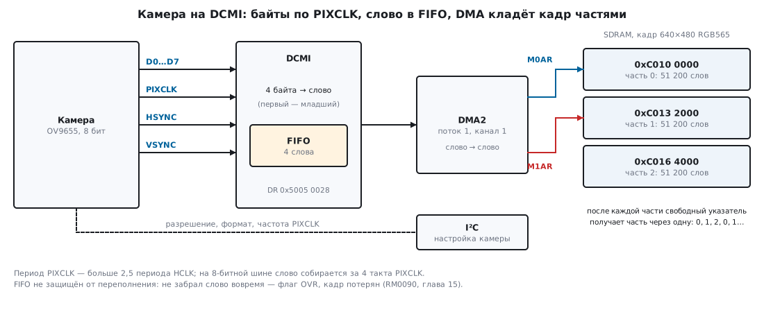
There are two sets of wires. The parallel bus goes from the camera to the DCMI: data D0–D13 (8, 10, 12 or 14 bits), PIXCLK, HSYNC and VSYNC. 11, 13, 15 or 17 inputs in total; the DCMI is always a slave, the camera sets the clock. The second bus is I²C: over it the program configures the camera — resolution, pixel format, PIXCLK frequency. The configuration is a long "register — value" table from the sensor documentation: in the BSP for the OV9655 in VGA mode it is 147 pairs, for the OV2640 it is 237.
22б.2 Signals, polarities and packing into words
The camera changes data on one edge of PIXCLK, the DCMI latches it on the other — which one is set by the PCKPOL bit. HSYNC and VSYNC divide the stream into lines and frames. The polarities VSPOL and HSPOL are defined in RM0090 like this: they are the level on the pin when data is not valid — that is, the blanking level, not "the level of the active line". Everything that arrives while HSYNC or VSYNC is at this level, the DCMI discards.
This is how the BSP and the Keil example set them:
| Board and camera | VSPOL | HSPOL | PCKPOL |
|---|---|---|---|
| STM324x9I-EVAL, OV2640 | low | low | rising |
| STM32746G-Discovery, OV9655 | high | low | rising |
| MCBSTM32F400, OVM7690 | high | low | rising |
For the OV2640 and OV9655 the BSPs set VSPOL differently: the bit depends on the camera and its configuration, and it is chosen for your camera, not taken from someone else's example.
Instead of HSYNC and VSYNC the camera can insert sync codes of the form 0xFF 00 00 XY into the stream (the ESS bit). This works only on an 8-bit bus, and then the values 0x00 and 0xFF are forbidden in the data.
Packing. On an 8-bit bus the DCMI assembles a word over four PIXCLK cycles, the first byte in the low bits; on 10, 12 and 14 bits over two cycles, one sample in each half of the word. Only when the word is ready does the DCMI ask DMA to take it. An RGB565 pixel is two cycles, there are two pixels in a word.
The frequency limit is not the bus but the clocking: the PIXCLK period must be greater than 2.5 HCLK periods. At an HCLK of 168 MHz this means PIXCLK below 67.2 MHz, at 216 MHz below 86.4 MHz; RM0090 and RM0385 limit the data rate itself to 54 MB/s.
22б.3 Snapshot and continuous capture
Snapshot (CM = 1). After CAPTURE is set the DCMI waits for the start of a frame, receives exactly one frame and clears CAPTURE itself. If an overrun happened on the way, the frame is lost and CAPTURE is cleared too — so after a snapshot the OVR flag is checked.
Continuous capture (CM = 0). Reception starts from the next VSYNC and goes frame after frame until CAPTURE is cleared; the clearing takes effect at the end of the current frame. The buffer, and whether it is linear or circular, is set by DMA, not by the DCMI. The FCRC field drops frames: all, every second one or one in four.
There are five interrupts: end of line (LINE), end of frame or window (FRAME), overrun (OVR), VSYNC and sync code error (ERR). The DCMI FIFO holds four words, and it has no overrun protection: if DMA has not taken a word in time, the FIFO is reset, and the DCMI waits for the next frame.
22б.4 The CROP window, JPEG and decimation on the F7
The window. DCMI_CWSTRT sets the start of the window: VST is the line number, HOFFCNT is how many PIXCLK cycles to skip in a line. DCMI_CWSIZE is the size: VLINE is lines, CAPCNT is PIXCLK cycles, both "minus one". An RGB565 pixel takes two cycles, and that is the main trap. The window width in cycles must add up to whole words: in the description of the window RM0090 writes that the two low bits of CAPCNT are cleared, and in the register description that CAPCNT is "minus one". There is no contradiction if CAPCNT + 1 is a multiple of four, as in the BSP below: 959 + 1 = 960.
The STM32746G-Discovery has a 480×272 screen, and the OV9655 cannot do that mode. The BSP
switches the camera to VGA and cuts out a window: VST 104, HOFFCNT 80, CAPCNT 959 —
that is 480 × 2 − 1 — VLINE 271. In registers this is CWSTRT 0x0068 0050 and
CWSIZE 0x010F 03BF. The window is 261 120 bytes, 0xFF00 words, as in GetSize of the BSP
for 480×272: one DMA transfer. Vertically the window is centred. Horizontally
the BSP passes half the difference of the widths in pixels, while the field counts
cycles: 80 cycles are 40 pixels. The window starts at pixel 40, and on the right
120 remain; for the centre HOFFCNT 160 is needed.
JPEG (the JPEG bit). The camera compresses the frame itself, VSYNC marks the start and end of the picture, HSYNC serves as a "data valid" signal. There is no window and no sync codes in this mode. The frame size is not known in advance: the buffer is taken with a margin, and how much arrived is computed from NDTR — it decreases with each transfer. If there were not enough bytes at the end to fill a word, the DCMI pads it with zeros. For uncompressed formats the limit is 2048 × 2048 pixels, for JPEG there is no limit.
Decimation on the F7. The F746 has fields in DCMI_CR that the F4 lacks. BSM takes every second byte, one in four or two in four, OEBS selects which one to start with; BSM works only on an 8-bit bus. From YCbCr 4:2:2 only the luma Y remains this way — a frame half the size. LSM and OELS take every second line.
22б.5 How much memory and what data rate
The memory DMA can write in one piece. On the F407 this is SRAM1 and SRAM2 — 128 KB: the 64 KB of CCM memory are not connected to the bus matrix (section 9). On the F429 SRAM3 is added to them — 192 KB. On the F746 it is 320 KB: DTCM, SRAM1 and SRAM2; DMA reaches DTCM through the core's AHBS slave bus (section 11б).
| Frame | Bytes | DMA words | F407, 128 KB | F429, 192 KB | F746, 320 KB |
|---|---|---|---|---|---|
| 160×120 RGB565 | 38 400 | 9 600 | yes | yes | yes |
| 320×240 RGB565 | 153 600 | 38 400 | no | yes | yes |
| 480×272 RGB565 | 261 120 | 65 280 | no | no | yes |
| 640×480 RGB565 | 614 400 | 153 600 | no | no | no |
| 640×480 Y8 | 307 200 | 76 800 | no | no | yes |
The word counts match GetSize in the BSP: 0x2580, 0x9600, 0xFF00 and
0x25800. A 320×240 frame does not fit into anything on the F407. The Keil example for the
MCBSTM32F400 does without a buffer: DMA with address increment switched off
writes the DCMI words directly to the data register of an 8080 display at 0x6C00 0002
(sections 22а and 41б). Through the stream FIFO each word goes out as two
16-bit writes — two pixels. VGA in 16 bits fits nowhere
except SDRAM: on the 746G-Discovery that is 8 MB from 0xC000 0000.
The data rate. Suppose the camera outputs a PIXCLK of 24 MHz on an 8-bit bus — this is an example, the frequency is set by the camera configuration. Within a line this is 24 MB/s, or six million words per second: one word every 28 HCLK cycles at 168 MHz and every 36 cycles at 216 MHz. The margin is the FIFO: four words are 16 PIXCLK cycles, 0.667 µs, or 112 cycles of a 168 MHz HCLK. That is how long DMA can wait for the bus while others hold it: LTDC, DMA2D, the processor. At the limit of 54 MB/s the margin is 0.296 µs. That is why the BSP gives the camera stream a high priority.
The pure data time of a frame at 24 MHz: 320×240 RGB565 — 6.4 ms, 640×480 — 25.6 ms. Even without blanking, VGA at this frequency gives no more than 39 frames per second.
22б.6 DMA: 65535 words and a double buffer
The DCMI request goes to DMA2, channel 1, stream 1 or 7 (RM0090, table 43; the same in RM0385). The direction is peripheral → memory, both widths are word, address increment only on the memory side. The BSPs of both boards use stream 1 in circular mode and FIFO direct mode.
The NDTR counter is 16-bit: no more than 65535 transfers per setup (section
9). A 640×480 RGB565 frame is 153 600 words. HAL gets around this with a double buffer:
if the length is greater than 0xFFFF, HAL_DCMI_Start_DMA halves it until the part
is no greater than 0xFFFF, and starts the stream with two pointers M0AR and
M1AR. In double-buffer mode DMA itself switches the pointer at the end of each part
and continues, and the handler DCMI_DMAXferCplt moves the free
pointer two parts ahead. A model of this handler on a PC:
| Frame | Words | Parts | Words each | Lost |
|---|---|---|---|---|
| 640×480 RGB565 | 153 600 | 4 | 38 400 | 0 |
| 640×480 Y8 | 76 800 | 2 | 38 400 | 0 |
| 800×600 RGB565 | 240 000 | 4 | 60 000 | 0 |
| window 330×399 RGB565 | 65 835 | 2 | 32 917 | 1 |
For VGA the model goes through parts 0, 1, 2, 3, 0, 1, 2, 3 — two frames in a row, as it should. But the division is integer: if the length does not divide by the number of parts, HAL simply loses the remainder, and DMA finishes the "frame" before the camera's frame ends.
At register level the frame can be split into any number of parts, as long as it divides exactly.
The functions camera_start and the interrupt handler of the example file split VGA into
three parts of 51 200 words:
#define CAM_FB      0xC0100000u         /* с 0xC000 0000 — буфер LTDC платы */
#define VGA_WORDS   FRAME_WORDS(640u, 480u, 2u)
#define PARTS       3u
#define PART        (VGA_WORDS / PARTS)
_Static_assert(VGA_WORDS == 153600u && VGA_WORDS % PARTS == 0u && PART <= 65535u,
               "кадр делится на части без остатка, часть — не больше 65535 слов");

static volatile uint32_t next_part;

void camera_start(void)
{
    dcmi_clocks();
    next_part = 2u;
    dma_dcmi(CAM_FB, CAM_FB + 4u * PART, PART, DMA_SxCR_DBM | DMA_SxCR_TCIE);
    NVIC_EnableIRQ(DMA2_Stream1_IRQn);
    dcmi_on(CR_POL);                    /* CM = 0: кадр за кадром */
    DCMI->CR |= DCMI_CR_CAPTURE;
}

void DMA2_Stream1_IRQHandler(void)      /* часть дописана: свободному указателю — часть через одну */
{
    uint32_t a = CAM_FB + 4u * PART * next_part;

    DMA2->LIFCR = DMA_LIFCR_CTCIF1;
    if (DMA2_Stream1->CR & DMA_SxCR_CT)
        DMA2_Stream1->M0AR = a;         /* DMA пишет по M1 — свободен M0 */
    else
        DMA2_Stream1->M1AR = a;
    next_part = (next_part + 1u) % PARTS;
}
M0AR may be written only while CT = 1, and M1AR only while CT = 0; otherwise RM0090 promises the TEIF error flag and the stream being disabled. Hence the CT check. The parts in the model go 0, 1, 2, 0, 1, 2 — an odd number of parts does not matter: frames simply start alternately with M0 and M1. armclang for the F746 turns the choice of pointer into a single conditional instruction without a branch:
LDR    r3,[r2,#0x20]       ; DMA2_Stream1->CR, r2 — адрес DMA2->LIFCR
MOV    r0,#0x32000         ; часть: 51 200 слов по 4 байта
LSLS   r3,r3,#12           ; бит 19 (CT) — в знак
MOV    r3,#0x2c            ; смещение M0AR от LIFCR
IT     PL
MOVPL  r3,#0x30            ; CT = 0 — M1AR
MOVT   r12,#0xc010         ; CAM_FB = 0xC010 0000
MLA    r0,r1,r0,r12        ; CAM_FB + next_part × 0x32000
STR    r0,[r3,r2]
The handler has the time of a whole part to change the pointer: 51 200 words at a
PIXCLK of 24 MHz are 8.533 ms. The frame lies from 0xC010 0000 to 0xC019 6000: the start of
SDRAM on the 746G-Discovery is taken by the LTDC buffer (LCD_FB_START_ADDRESS
0xC000 0000; 480×272 in 32 bits is 0x7F800 bytes).
For the F407 the same file has a 160×120 snapshot into internal SRAM in one
transfer, the function camera_snapshot. It shows what the fields add up to:
NDTR 0x2580, SxCR 0x0202 5400 (channel 1, high priority, words,
memory increment), DCMI_CR 0x40A2 (ENABLE, VSPOL, PCKPOL, CM).
22б.7 Pitfalls
- VSYNC polarity "the wrong way round". VSPOL and HSPOL are the level when data is not valid. Mix them up and the DCMI receives blanking instead of the frame: the FRAME flag comes, but the buffer holds garbage or a shifted image.
- HOFFCNT in pixels instead of cycles. The field counts PIXCLK cycles, and RGB565 has two per pixel. The 746G-Discovery BSP passes 80 — by the document the window starts at pixel 40, not in the centre.
- A frame of more than 65535 words in one transfer. NDTR is 16-bit: VGA RGB565 is 153 600 words, only in parts through a double buffer.
- The length does not divide into parts. HAL halves it with integer division and throws the remainder
away: for a 330×399 window this is one word per frame. The window size
is chosen so that the word count divides, or you split it yourself, as in
camera_start. - Writing M0AR or M1AR at the wrong time. Only the pointer DMA is not writing through right now may be touched: check CT. Otherwise TEIF and the stream stops.
- FIFO overrun. Four words are 0.667 µs at 24 MHz. Long bursts of other masters into the same SDRAM or a low stream priority — and the OVR flag, the frame is lost. After a snapshot checking OVR is mandatory. In continuous capture DMA does not know about the FIFO reset and will continue counting from the middle of a part — on OVR the DMA stream is restarted.
- A buffer in CCM on the F4. CCM is not connected to the bus matrix, DMA does not write there (section 9). Of the F407's 192 KB of RAM, 128 are available to the camera.
- Accessing DCMI registers other than as words. The RM requires 32-bit access, a byte or half-word gives a bus error.
- The camera's I²C address. The BSP passes 0x60: HAL takes the address already shifted left, it is the seven-bit 0x30. The Keil driver for the OVM7690 writes the seven-bit 0x21.
- Cache on the F7. A buffer in SRAM1 or SRAM2 of the F746 is cached, DTCM is not:
before the processor reads the frame, the buffer lines are invalidated with
SCB_InvalidateDCache_by_Addr(section 11б). SDRAM at 0xC000 0000 is by default Device, uncached (section 41б).
22б.8 Summary
- DCMI is on the F407/F417, F42x/F43x, F446, F469/F479 and on the F745 and above; the F401, F405, F410–F413 do not have it. The camera is configured over I²C, the DCMI only receives.
- Signals: D0–D13, PIXCLK, HSYNC, VSYNC — 11…17 inputs; VSPOL/HSPOL are the blanking level; the PIXCLK period is greater than 2.5 HCLK periods: up to 67.2 MHz at 168 MHz.
- 8 bits — a word per 4 PIXCLK cycles, a 4-word FIFO with no protection; at 24 MHz the DMA margin is 0.667 µs.
- Frame: 320×240 RGB565 is 153 600 bytes, it does not fit into the 128 KB of the F407; 640×480 is 614 400 bytes, only in SDRAM.
- The window is counted in PIXCLK cycles: for RGB565 multiply width and offset by 2; 480×272 out of VGA is 0xFF00 words.
- NDTR up to 65535: VGA is 153 600 words, HAL splits it into 4 parts of 38 400, at register level into 3 of 51 200; the length must divide exactly.
Full sources
dcmi22b.c — DCMI at register level: a snapshot on the F407 and continuous capture on the F746.
/* 22б: DCMI по регистрам — снимок QQVGA во внутреннюю SRAM на F407
   и непрерывный VGA в SDRAM на F746 с двойным буфером DMA.
   Собирается armclang: -DSTM32F407xx и -DSTM32F746xx.
   Выводы (GPIO, AF13) и настройка камеры по I²C — вне этого файла. */
#include <stddef.h>
#include <stdint.h>

/* поля DCMI и DMA — RM0090, 15.8 и 10.5; у RM0385 для F7 они те же */
_Static_assert(DCMI_BASE == 0x50050000u && offsetof(DCMI_TypeDef, DR) == 0x28u, "DCMI на AHB2, DR по 0x50050028");
_Static_assert(DCMI_CR_CAPTURE == (1u << 0) && DCMI_CR_CM == (1u << 1) && DCMI_CR_CROP == (1u << 2)
               && DCMI_CR_JPEG == (1u << 3), "CAPTURE, CM, CROP, JPEG — биты 0…3");
_Static_assert(DCMI_CR_PCKPOL == (1u << 5) && DCMI_CR_HSPOL == (1u << 6) && DCMI_CR_VSPOL == (1u << 7),
               "полярности PCKPOL, HSPOL, VSPOL — биты 5, 6, 7");
_Static_assert(DCMI_CR_ENABLE == (1u << 14) && DCMI_CWSTRT_VST_Pos == 16u && DCMI_CWSIZE_VLINE_Pos == 16u,
               "ENABLE — бит 14; строки окна — в старшей половине CWSTRT и CWSIZE");
_Static_assert(DMA_SxCR_CHSEL_Pos == 25u && DMA_SxCR_DBM == (1u << 18) && DMA_SxCR_CT == (1u << 19),
               "канал в битах 27:25, DBM — бит 18, CT — бит 19");

#define FRAME_WORDS(w, h, bytes_per_px) ((w) * (h) * (bytes_per_px) / 4u)

/* VSYNC активен высоким, HSYNC — низким, захват по фронту PIXCLK:
   так у STM32746G-Discovery (OV9655) и у MCBSTM32F400 (OVM7690) */
#define CR_POL (DCMI_CR_PCKPOL | DCMI_CR_VSPOL)

static void dcmi_clocks(void)          /* такты — раньше любой записи в DMA2 и DCMI */
{
    RCC->AHB1ENR |= RCC_AHB1ENR_DMA2EN;
    RCC->AHB2ENR |= RCC_AHB2ENR_DCMIEN;
    (void)RCC->AHB2ENR;
}

static void dcmi_on(uint32_t cr)
{
    DCMI->CR = cr;                      /* всё настроить до ENABLE */
    DCMI->CR = cr | DCMI_CR_ENABLE;
}

/* DMA2, поток 1, канал 1 — запрос DCMI (RM0090, таблица 43) */
static void dma_dcmi(uint32_t m0, uint32_t m1, uint32_t items, uint32_t extra)
{
    DMA_Stream_TypeDef *s = DMA2_Stream1;

    s->CR = 0;
    while (s->CR & DMA_SxCR_EN) {
    }
    DMA2->LIFCR = DMA_LIFCR_CTCIF1 | DMA_LIFCR_CHTIF1 | DMA_LIFCR_CTEIF1 | DMA_LIFCR_CDMEIF1 | DMA_LIFCR_CFEIF1;
    s->PAR  = (uint32_t)&DCMI->DR;
    s->M0AR = m0;
    s->M1AR = m1;
    s->NDTR = items;                    /* слов, не больше 65535 */
    s->FCR  = 0;                        /* прямой режим, как в BSP */
    s->CR   = (1u << DMA_SxCR_CHSEL_Pos) | DMA_SxCR_PL_1 | DMA_SxCR_MSIZE_1 | DMA_SxCR_PSIZE_1
            | DMA_SxCR_MINC | extra;    /* DIR = 00: периферия → память, слова */
    s->CR  |= DMA_SxCR_EN;
}

#if defined(STM32F407xx)
/* ── снимок 160×120 RGB565: 38 400 байт — во внутреннюю SRAM, одной передачей ── */
#define QQVGA_WORDS FRAME_WORDS(160u, 120u, 2u)
_Static_assert(QQVGA_WORDS == 9600u && QQVGA_WORDS <= 65535u, "QQVGA — 9600 слов, одна передача DMA");

static uint32_t qqvga[QQVGA_WORDS];

int camera_snapshot(void)               /* 0 — кадр в qqvga, -1 — переполнение FIFO */
{
    dcmi_clocks();
    DCMI->ICR = DCMI_ICR_FRAME_ISC | DCMI_ICR_OVR_ISC;
    dma_dcmi((uint32_t)qqvga, 0u, QQVGA_WORDS, 0u);
    dcmi_on(CR_POL | DCMI_CR_CM);       /* CM = 1: один кадр */
    DCMI->CR |= DCMI_CR_CAPTURE;        /* ждёт начала кадра */
    while (DCMI->CR & DCMI_CR_CAPTURE) {
    }                                   /* в конце кадра бит снимается сам */
    return (DCMI->RISR & DCMI_RIS_OVR_RIS) ? -1 : 0;
}

#elif defined(STM32F746xx)
/* ── непрерывно 640×480 RGB565: 614 400 байт — только в SDRAM (0xC000 0000, 8 МБ) ── */
#define CAM_FB      0xC0100000u         /* с 0xC000 0000 — буфер LTDC платы */
#define VGA_WORDS   FRAME_WORDS(640u, 480u, 2u)
#define PARTS       3u
#define PART        (VGA_WORDS / PARTS)
_Static_assert(VGA_WORDS == 153600u && VGA_WORDS % PARTS == 0u && PART <= 65535u,
               "кадр делится на части без остатка, часть — не больше 65535 слов");

static volatile uint32_t next_part;

void camera_start(void)
{
    dcmi_clocks();
    next_part = 2u;
    dma_dcmi(CAM_FB, CAM_FB + 4u * PART, PART, DMA_SxCR_DBM | DMA_SxCR_TCIE);
    NVIC_EnableIRQ(DMA2_Stream1_IRQn);
    dcmi_on(CR_POL);                    /* CM = 0: кадр за кадром */
    DCMI->CR |= DCMI_CR_CAPTURE;
}

void DMA2_Stream1_IRQHandler(void)      /* часть дописана: свободному указателю — часть через одну */
{
    uint32_t a = CAM_FB + 4u * PART * next_part;

    DMA2->LIFCR = DMA_LIFCR_CTCIF1;
    if (DMA2_Stream1->CR & DMA_SxCR_CT)
        DMA2_Stream1->M0AR = a;         /* DMA пишет по M1 — свободен M0 */
    else
        DMA2_Stream1->M1AR = a;
    next_part = (next_part + 1u) % PARTS;
}
#endif
Next: section 22в "Segment LCD: the glass, multiplexing and the LCD controller" — a display that draws almost no current: multiplexing, bias and the built-in LCD controller.