 Embedded HandbookApps
41а. SD card over SDIO: four data lines, commands, DMA and FatFS
In section 41 the card is connected over SPI — four wires, any microcontroller, a speed of about 3 MB/s at best. The F4 (and the high-density F103) has its own SDIO block: it talks to the card in the card's native protocol, drives data over four lines at once, computes the checksums in hardware and feeds DMA. The same FatFS on top of it runs several times faster. The price is three extra wires, pull-ups and a startup protocol you need to understand when the card "is not detected".
The protocol rules, the divider formula, the FIFO structure and the DMA procedure
are taken from the F4 reference manual (from the Keil pack); the startup command
sequence is from the HAL 2.17.1 sources. Times, CRCs and dividers were recomputed
by the program _verify/sdio41a/sdio_calc.c, built with gcc on a PC. The check is
_verify/sdio41a_check.py.
Terms used in the documentation
Term Meaning SDIO, SDMMC the block for SD/MMC cards (called SDMMC in newer families) SDIO_CK, SDIO_CMD, SDIO_D0…D3 clock, command line, data lines CPSM, DPSM the command and data state machines inside the block command, response (R1…R7) a command and the card's answer ACMD an "application" command — it comes after CMD55 OCR, CID, CSD, RCA, SCR card registers: power, identity, parameters, address, capabilities SDSC, SDHC/SDXC standard-capacity and high-capacity card block, DBLOCKSIZE a data block and the code for its size wide bus four-bit mode
41а.1 How SDIO differs from a card over SPI
The card has two faces. In SPI mode it pretends to be an ordinary slave device:
one line in, one line out, a chip select. In native mode it has a separate
command line CMD, a clock CLK and up to four data lines D0…D3; bits go
over all four at the same time. The SDIO block knows only the native mode — it has no
SPI mode, and the manual says so directly.
What this gives at 24 MHz (the default working clock in HAL):
| Mode | One 512-byte block | Data phase limit |
|---|---|---|
| SDIO, 1 line | 4114 clocks — 171.4 µs | 3.0 MB/s |
| SDIO, 4 lines | 1042 clocks — 43.4 µs | 11.8 MB/s |
| SPI at 25 Mbit/s | ≈ 4100 clocks | ≈ 3 MB/s |
A block is a start bit, 4096 data bits, 16 CRC bits on each line and a stop bit: on four lines the data is divided by four, and the checksums are computed in parallel. Hence the almost fourfold gain.
That is the limit of the data transfer itself. The real throughput also includes the command
and the response of 48 bits each, the card's access time before the first block, and for writes the time
while the card holds D0 "busy": on cheap cards that is milliseconds per block.
Only multi-block reads come close to the calculation.
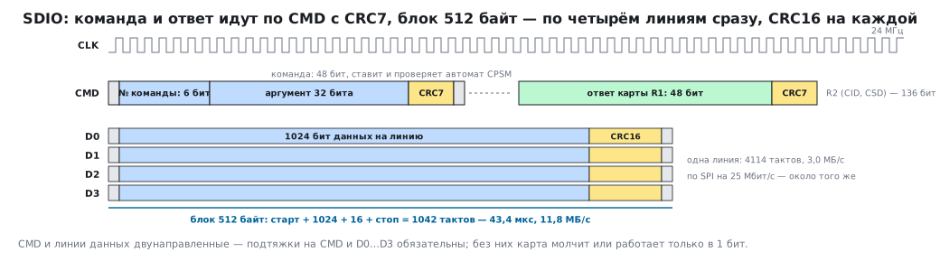
Two more differences: checksums are always on — CRC7 for commands and responses,
CRC16 for each data line, and the block computes them itself; and the lines are bidirectional and
need pull-ups to the supply on all of D0…D3 and CMD — the manual requires external
resistors on the data lines. Without them the card is silent or works only in
one-bit mode.
The F411 has an SDIO block (the datasheet calls it "SD/MMC/eMMC"), and so do the F407 and F429; the BluePill on the F103C8 does not have one — only SPI there (section 41).
41а.2 Clock: the divider and two frequency modes
The card clock is derived from SDIOCLK by the divider in the CLKCR register:
SDIO_CK = SDIOCLK / (CLKDIV + 2)
SDIOCLK is the same 48 MHz used for USB (the manual: up to 50 MHz, 48 when working
together with USB), so the PLL must deliver a true 48 MHz, otherwise the card gets
the wrong frequency. There is also a divider bypass mode — then the card is clocked directly from
SDIOCLK.
HAL keeps two dividers:
#define SDIO_INIT_CLK_DIV     ((uint8_t)0x76)    /* 48MHz / (SDMMC_INIT_CLK_DIV + 2) < 400KHz */
#define SDIO_TRANSFER_CLK_DIV ((uint8_t)0x0)     /* 48MHz / (SDMMC_TRANSFER_CLK_DIV + 2) < 25MHz */
0x76 is 118: 48 MHz / 120 = exactly 400 kHz, the limit for talking to the card during
startup. 0 gives 48 / 2 = 24 MHz for data transfer. Starting at a low frequency is
not a whim of HAL but a requirement of the card: at 24 MHz it will not answer the first commands,
and the symptom will be "the card is not detected", with different cards behaving differently.
41а.3 Command and response
A command is always 48 bits on the CMD line: a start bit, a direction bit, 6 bits of
command number, 32 bits of argument, CRC7 and a stop bit. Responses are short —
also 48 bits — or long, 136 bits: that is how the card returns the CID and CSD registers. The hardware
(the command state machine, CPSM) inserts the CRC7 itself and checks it in the response; the exception is
the R3 power response, where the CRC field is filled with ones and is not checked.
The frames of the first commands are the same as those computed by hand in 18.10 for SPI
mode: CMD0 — CRC 0x95, CMD8 with argument 0x1AA — 0x87. Only here they are
computed by the block, not by the program.
The responses you meet during startup:
| Response | Length | What it carries |
|---|---|---|
| R1 | 48 | the command number and the card state |
| R2 | 136 | CID (identity) or CSD (parameters) |
| R3 | 48 | OCR: voltage window, readiness, SDHC flag |
| R6 | 48 | the published RCA address |
| R7 | 48 | the answer to CMD8: voltage and the echoed pattern |
Some commands are application commands, ACMD: their number can be the same as an ordinary
command (ACMD41, ACMD6, ACMD51), and the card tells them apart only by the fact that
a CMD55 with its address came before them. Without CMD55 the card executes the same number as
an ordinary command — or answers with an error.
41а.4 Starting the card: what HAL_SD_Init does
HAL_SD_Init calls HAL_SD_InitCard, and that contains the whole startup protocol, in the same
order as over SPI in section 41, but with different responses:
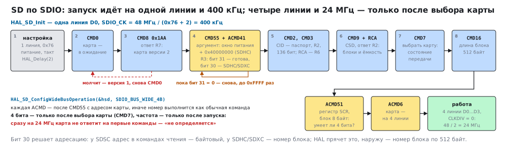
- The block is set to 1 bit and
SDIO_INIT_CLK_DIV, pin power and the clock are switched on, then a pauseHAL_Delay(2)— the card needs time after the clock is applied. CMD0— the card goes to the idle state.CMD8with the pattern0x1AA. If it answered, it is a version 2 card; if not, version 1, andCMD0is repeated.CMD55+ACMD41in a loop — up to0xFFFFattempts: the argument carries the voltage window and bit0x40000000"the host supports SDHC". In the response bit 31 means "ready"; while it is zero, the loop goes on. Bit 30 in a ready card's response isSDHC/SDXC, otherwiseSDSC.CMD2— the card returns its CID (136 bits),CMD3— it publishes its RCA address.CMD9with the RCA — the CSD: from it HAL computes the number of blocks and the capacity.CMD7— select the card: it goes to the transfer state.CMD16— block length 512.
After that HAL_SD_ConfigWideBusOperation(&hsd, SDIO_BUS_WIDE_4B) reads
the SCR register (ACMD51, an 8-byte block), makes sure the card supports 4 bits, sends
ACMD6 and reconfigures the block to four lines and the working divider. The order
cannot be swapped: 4 bits are enabled only after the card is selected, and the frequency
is raised only after startup.
if (HAL_SD_Init(&hsd) != HAL_OK)                  /* 1 бит, 400 кГц, весь протокол */
    return -1;
if (HAL_SD_ConfigWideBusOperation(&hsd, SDIO_BUS_WIDE_4B) != HAL_OK)
    return -2;                                    /* 4 линии, 24 МГц */
In hsd.Init.BusWide itself you leave SDIO_BUS_WIDE_1B: right after
CMD7 HAL reconfigures the block from hsd.Init — both the divider and the bus width.
With SDIO_BUS_WIDE_4B there, the block would switch to four lines before the card (41а.7).
Capacity and addressing: on SDSC the address in read commands is a byte address, on SDHC/SDXC it is
a block number; HAL hides this inside HAL_SD_ReadBlocks, and what you always see outside is
a block number in 512-byte blocks.
41а.5 Data block, FIFO and DMA
Data travels in 512-byte blocks — exactly a FAT sector. In the data control
register the size is encoded as a power of two: DBLOCKSIZE = 0x9 means 2⁹ = 512.
Inside the block there is a FIFO of 32 words of 32 bits; the "half" flag — 8 words — serves as the
DMA request. The CPU can read the FIFO (HAL_SD_ReadBlocks does exactly that),
but at 24 MHz on four lines a word arrives every 333 ns, and the CPU is
busy with nothing else.
The right way is DMA, and the manual gives an exact recipe for it: DMA2, stream 3 or
stream 6, channel 4; 32-bit words; the peripheral is the flow controller
(PFCTRL: the length is known by SDIO, not by DMA); bursts of 4 words at least on the
peripheral side. The order when writing a block: start DMA, send CMD24, wait for
CMDREND, enable the data state machine with DMAEN, wait for DBCKEND.
HAL_SD_WriteBlocks_DMA and HAL_SD_ReadBlocks_DMA do this themselves; the program
has to provide two handlers — SDIO_IRQHandler and the DMA stream interrupt — and a buffer
aligned to 4 bytes.
The data checksums are CRC16 with polynomial 0x1021, one for each line.
A block of 512 bytes of 0xFF on one line gives 0x7FA1 (in four-bit mode
each line carries 128 bytes of 0xFF, and the per-line sum is 0xEDA9) — the number everyone who has written a card driver by hand
uses to check their implementation; here the hardware computes it, and
an error arrives as the DCRCFAIL flag. The second guard is the data timer DTIMER: if the card
has not answered a read or holds the line "busy" longer than set, the block raises
DTIMEOUT instead of waiting forever.
41а.6 FatFS on top of SDIO
The disk layer for FatFS (section 42) is the same five functions as for SPI, only with HAL inside them:
static volatile int rx_done;

void HAL_SD_RxCpltCallback(SD_HandleTypeDef *h) { (void)h; rx_done = 1; }

DRESULT disk_read(BYTE pdrv, BYTE *buf, LBA_t sector, UINT count)
{
    (void)pdrv;
    rx_done = 0;
    if (HAL_SD_ReadBlocks_DMA(&hsd, buf, (uint32_t)sector, count) != HAL_OK)
        return RES_ERROR;
    uint32_t t0 = HAL_GetTick();
    while (!rx_done)                                            /* DMA перенёс всё */
        if (HAL_GetTick() - t0 > 1000u) return RES_ERROR;
    while (HAL_SD_GetCardState(&hsd) != HAL_SD_CARD_TRANSFER)   /* карта снова готова */
        if (HAL_GetTick() - t0 > 1000u) return RES_ERROR;
    return RES_OK;
}
HAL_SD_ReadBlocks_DMA only starts the exchange and returns immediately. The end of
the transfer is marked by the callback HAL_SD_RxCpltCallback: it is called from the DMA
interrupt when the last word has landed in memory, and for multi-block reads HAL
sends CMD12 itself before it. So you first wait for the callback and only then for
the TRANSFER state: that state is about the card, not about memory — DMA may not yet have
unloaded the tail of the FIFO, and polling with CMD13 in the middle of the exchange collides with the CMD12
from the interrupt. Both waits have a timeout, otherwise a removed card will hang
the program forever.
disk_write works the same way, with HAL_SD_TxCpltCallback, and there the wait for TRANSFER
is doubly mandatory: the card answers "accepted" before it has physically written
the block, and the next command without this pause gets a "busy" error. The buffer from
FatFS can be unaligned, while DMA needs an address that is a multiple of 4 (41а.5): you check
((uintptr_t)buf & 3) != 0 and in that case send the sectors one at a time through your own
aligned buffer. The sector size is 512, the number of sectors comes from HAL_SD_GetCardInfo,
LogBlockNbr. Everything else in FatFS does not depend on the bus.
41а.7 Pitfalls
| Symptom | Cause |
|---|---|
| the card does not answer at all | no pull-ups on CMD and D0…D3 — the lines are bidirectional |
| works with 1 bit, CRC errors with 4 bits | pull-ups only on D0; or D1…D3 are taken by another peripheral |
HAL_SD_Init passed, but the very first read fails |
hsd.Init.BusWide is SDIO_BUS_WIDE_4B: after CMD7 HAL switched the block to four lines, while the card, without ACMD6, stayed on one |
| "not detected" on some cards, works on others | startup at the working frequency right away instead of 400 kHz |
| the clock frequency is not what was calculated | SDIOCLK comes from the 48 MHz PLL output, and that is not configured |
ACMD41 loops until timeout |
no CMD55 before the application command; or a version 1 card that does not answer CMD8 |
| DMA transfers garbage or hangs | not stream 3/6 of DMA2, no PFCTRL, the buffer is not aligned to 4 bytes |
| a write returns "busy" every other time | the next command before the card has gone to TRANSFER |
disk_read returned success, but the buffer is incomplete |
you waited only for TRANSFER, not for the end-of-DMA callback |
| the card was removed and the program hangs | waiting for the callback or for TRANSFER without a timeout |
| after a write the data reads back old | the SDIO_IRQHandler and DMA stream handlers are not connected — the callbacks never arrive |
| CRC errors on long wires | 24 MHz over a ribbon cable: lower it with the divider or shorten the wires |
DCRCFAIL on writes with short wires |
the F4 has hardware flow control enabled (HWFC_EN, bit 14 of SDIO_CLKCR) or NEGEDGE: according to the errata both corrupt data — do not enable them |
| a reset when accessing the card | current peak of up to 100 mA, no capacitor at the holder (section 41) |
41а.8 Summary
- SDIO is the card's native protocol:
CMD,CLK, up to four data lines; the block has no SPI mode; pull-ups onCMDand allDlines are mandatory. - Clock:
SDIO_CK = SDIOCLK / (CLKDIV + 2)from 48 MHz; startup at 400 kHz (CLKDIV = 0x76), work at 24 MHz (CLKDIV = 0). - A command is 48 bits with CRC7; responses are 48 or 136 bits;
ACMDcommands come afterCMD55. - Startup:
CMD0 → CMD8 → ACMD41 (bit 31 ready, bit 30 SDHC) → CMD2 → CMD3 →
  CMD9 → CMD7 → CMD16
; 4 bits only after the card is selected (ACMD6). - A 512-byte block (
DBLOCKSIZE 0x9), a FIFO of 32 words, DMA2 stream 3/6 channel 4 with the peripheral as flow controller and bursts of 4; on four lines a block takes 43.4 µs, 11.8 MB/s versus 3 over SPI. - CRC16
0x1021on each line,0x7FA1for 512 bytes of0xFF; a data timer instead of waiting forever. - FatFS:
disk_read/writethroughHAL_SD_*Blocks_DMA: wait for the end-of-transfer callback, then forTRANSFER, both times with a timeout; an unaligned FatFS buffer goes through your own.
Next: section 41б "FSMC and FMC: 8080 display, external SRAM and SDRAM" — a parallel bus on which external memory and a display become a range of addresses.