 Embedded HandbookApps
41б. FSMC and FMC: 8080 display, external SRAM and SDRAM
Section 41 gave FSMC one row of a table: a parallel bus for SRAM, NOR, NAND and SDRAM. Section 22а connects a display with its own controller to it: a command and a pixel are each a write to one of two addresses. Here is how it works: where these addresses come from, how to count timings in bus clocks, how external SRAM differs from SDRAM, and why SDRAM has to be started step by step and refreshed.
Sources: the reference manual RM0090 (F405/F407 and F427/F429, the FSMC and FMC chapters), the Cortex-M7 core manual (DUI 0646B) and RM0385 for the F7. The board numbers come from the board support packages (BSP) in the Keil packs: STM32412G-Discovery (display), STM324xG-EVAL (SRAM), STM32F429I-Discovery and STM32746G-Discovery (SDRAM). The code is built with armclang for the F407 and F429; the calculations are done by a script on a PC. QEMU does not model external buses — this was checked against the documents, not by running it.
Terms used in the documentation
Term Meaning FSMC (flexible static memory controller) a static memory controller: SRAM, NOR, NAND, PC Card FMC (flexible memory controller) the same plus an SDRAM controller NE1…NE4 chip selects in bank 1: four regions of 64 MB HADDR the internal AHB bus address ADDSET, DATAST the address phase and the data phase, in HCLK cycles BUSTURN the pause between accesses, in HCLK cycles extended mode, mode A separate read and write timings SDRAM refresh recharging the rows of dynamic memory CAS latency the delay before data comes out after a column read command
41б.1 Where FSMC and FMC exist
FSMC is on the high-density F103 (section 41) and on the F405/F407; the BluePill does not have it. FMC is on the F427/F429, F7 and H7: an SDRAM controller is added to the same static memory banks. To the program both look the same: external memory is a range of addresses, and a read or write there becomes a cycle on the pins. The controller itself drives the address, the chip select and the read and write strobes, waits the configured clocks and picks up the data. Not a single line of code per bus cycle — only the timing setup.
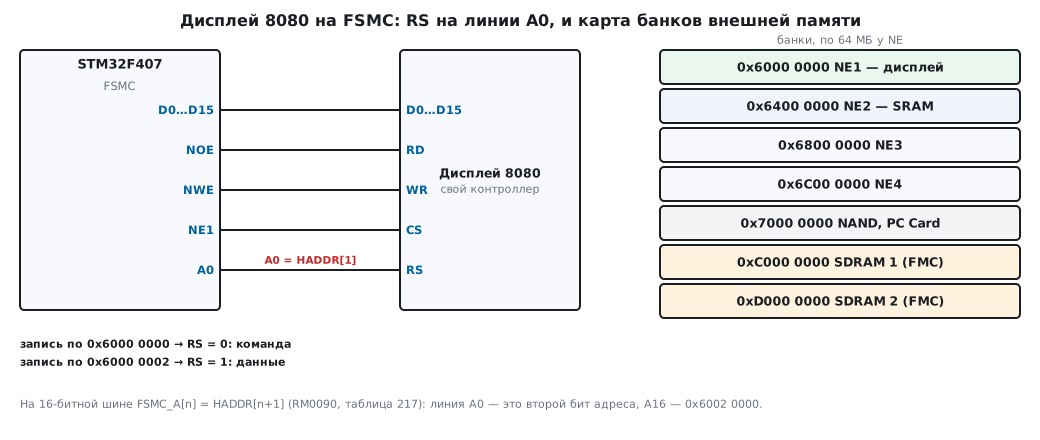
The banks in RM0090 (table 218 and its neighbours):
| Addresses | Bank | What is connected |
|---|---|---|
| 0x6000 0000–0x6FFF FFFF | bank 1: NE1…NE4, 64 MB each | SRAM, PSRAM, NOR, 8080 display |
| 0x7000 0000, 0x8000 0000 | banks 2 and 3 | NAND |
| 0x9000 0000 | bank 4 | PC Card |
| 0xC000 0000, 0xD000 0000 | SDRAM banks 1 and 2 (FMC only) | SDRAM |
41б.2 Addresses: bank, NE and the shift on a 16-bit bus
Address bits HADDR[27:26] select one of the four chips of bank 1 (RM0090, table 216): NE1 — 0x6000 0000, NE2 — 0x6400 0000, NE3 — 0x6800 0000, NE4 — 0x6C00 0000. Each gets 64 MB of addresses.
The subtlety is in the bus width (table 217). HADDR addresses bytes, while a 16-bit memory addresses words. So on a 16-bit bus the controller puts HADDR[25:1] on the FSMC_A[24:0] lines: line A0 is address bit 1, A16 is bit 17. This gives the addresses of a display whose RS input ("command or data") is tied to a single address line:
| Select | RS on line | Command | Data |
|---|---|---|---|
| NE1 | A0 | 0x6000 0000 | 0x6000 0002 |
| NE1 | A16 | 0x6000 0000 | 0x6002 0000 |
| NE1 | A18 | 0x6000 0000 | 0x6008 0000 |
| NE4 | A6 | 0x6C00 0000 | 0x6C00 0080 |
| NE4 | A10 | 0x6C00 0000 | 0x6C00 0800 |
For A16 the naive calculation 1 << 16 gives 0x6001 0000 — that is still a command:
line A16 is zero. The shift by one is the thing people forget most often.
Examples for cheap boards use the base 0x6C00 007E. It is the same
calculation: a structure of two 16-bit fields {REG; RAM} placed at
0x6C00 007E puts REG at 0x6C00 007E (A6 = 0) and RAM at 0x6C00 0080
(A6 = 1) — RS on line A6.
41б.3 An 8080 display through FSMC
On the STM32412G-Discovery the display sits on NE1, with RS on line A0 (pin PF0). The BSP describes it with a two-field structure — and then a command and data are written with an ordinary assignment:
typedef struct {
    volatile uint16_t REG;              /* 0x60000000: A0 = 0 — команда */
    volatile uint16_t RAM;              /* 0x60000002: A0 = 1 — данные  */
} lcd_t;
#define LCD ((lcd_t *)0x60000000u)

_Static_assert(offsetof(lcd_t, RAM) == 2, "на 16-битной шине A0 = HADDR[1]: данные на 2 байта выше");

void lcd_cmd(uint8_t c)   { LCD->REG = c; }
void lcd_data(uint16_t d) { LCD->RAM = d; }
armclang for the F407 turns each function into a single 16-bit write:
lcd_cmd:   MOV   r1,#0x60000000
           STRH  r0,[r1,#0]
lcd_data:  MOVS  r1,#2
           MOVT  r1,#0x6000
           STRH  r0,[r1,#0]
volatile is mandatory here (section 124): without it the compiler may merge two
consecutive writes to the RAM address into one, and for a display those are two pixels.
The register-level bank setup is in the fsmc_lcd_init function of the example file:
the timings in BTR1 and BWTR1 (41б.4) and BCR1 with a 16-bit width, write
enable and separate timings (EXTMOD). The pins use alternate function
AF12; it is easier to leave them to CubeMX.
A write over the bus does not keep the CPU waiting longer than the cycle lasts — and it can be handed to DMA in "memory to memory" mode (section 9): the source is a line buffer in RAM, the destination is the RAM address without increment.
41б.4 Timings: mode A in HCLK cycles
An asynchronous cycle consists of phases, each an integer number of HCLK cycles. In mode A (separate read and write timings, EXTMOD = 1) RM0090 gives (tables 229–230):
- read: ADDSET + DATAST cycles, the NOE strobe is low for DATAST;
- write: ADDSET + (DATAST + 1) cycles, the NWE strobe is low for DATAST + 1;
- BUSTURN is the pause between accesses.
The read timings are in BTR1, the write timings in BWTR1. A display usually reads much more slowly than it writes, and that is exactly why mode A is used: the same numbers for both directions would either slow down writes or break reads.
The STM32412G-Discovery BSP sets (a 10 ns cycle at an HCLK of 100 MHz — the maximum frequency of the F412):
| ADDSET | DATAST | Cycles | Cycle time | |
|---|---|---|---|---|
| read | 9 | 36 | 45 | 450 ns |
| write | 1 | 7 | 9 | 90 ns |
How to get the numbers for your own display: from its documentation take the minimum write cycle time and the minimum low time on WR, and divide by the HCLK period, rounding up: DATAST + 1 must be no less than the WR low time, ADDSET + DATAST + 1 no less than the cycle. For reads, the same with the read cycle. A margin of a cycle is fine; a shortfall gives errors that do not show up right away but only on some of the pixels.
The limit on image speed is the number of writes per bus cycle. At 90 ns per write (16 bits per pixel, one write per pixel):
| Screen | Writes | Frame time | No more than frames/s |
|---|---|---|---|
| 240×240 | 57600 | 5.184 ms | 192 |
| 320×240 | 76800 | 6.912 ms | 144 |
| 480×320 | 153600 | 13.824 ms | 72 |
This is the ceiling of the bus; the program loop or DMA adds its own overhead.
41б.5 External SRAM
Static memory is connected the same way as a display, only with many address lines. The STM324xG-EVAL has a 2 MB IS61WV102416BLL SRAM (16 bits) on NE2 — address 0x6400 0000. The BSP sets ADDSET 2, DATAST 2, BUSTURN 1 in mode A; at an HCLK of 168 MHz that is 4 cycles (23.8 ns) for a read and 5 cycles (29.8 ns) for a write.
Such memory looks like an ordinary array: you can put the heap, a frame buffer or large tables there — through a linker section (section 11) or simply with a pointer. It is slower than the internal SRAM: the controller splits each 32-bit access to a 16-bit memory into two bus cycles (RM0090, the transaction rules in 36.3.1).
41б.6 SDRAM on FMC: startup and refresh
SDRAM is cheaper than SRAM of the same size, but it is dynamic: the cells discharge, and every row has to be refreshed at least once per refresh period (usually 64 ms for all rows). Its address is multiplexed: row, then column. So FMC has a separate SDRAM controller with its own registers SDCR, SDTR, SDCMR and SDRTR.
On the STM32F429I-Discovery the IS42S16400J SDRAM is on bank 2 — address 0xD000 0000:
12 row bits, 8 column bits, 4 banks, a 16-bit bus. The size is
4096 × 256 × 4 × 2 = 8388608 bytes = 0x80 0000, as in SDRAM_DEVICE_SIZE
in the BSP. SDCLK is HCLK / 2.
Startup according to RM0090 takes eight steps:
- SDCR: SDCLK frequency, burst reads RBURST, the RPIPE delay, rows, columns, width, banks, CAS.
- SDTR: the memory timings.
- The "Clock Configuration Enable" command — SDCLK starts going to the memory.
- A pause: usually about 100 µs (per the memory documentation).
- The "Precharge All" command — close all rows.
- The "Auto-refresh" command — usually 8 times in a row (the NRFS field).
- The "Load Mode Register" command: burst length 1 and CAS as in SDCR.
- The refresh counter in SDRTR.
At register level this is the sdram_init function of the example file. Two things in it are easy
to miss. The SDCLK frequency, RBURST and RPIPE are written only into SDCR1, and TRC and TRP
only into SDTR1, even when the memory is on bank 2: in SDCR2 and SDTR2 these fields
have no effect. And the timing fields take "cycles minus one": a TRC of 7 cycles
is 6 in the field (HAL does the same).
The F429I-Discovery BSP timings at an SDCLK of 90 MHz (11.1 ns):
| Parameter | Cycles | ns |
|---|---|---|
| TMRD (after Load Mode) | 2 | 22.2 |
| TXSR (exit from self-refresh) | 7 | 77.8 |
| TRAS (row open) | 4 | 44.4 |
| TRC (row to row) | 7 | 77.8 |
| TWR (after a write) | 2 | 22.2 |
| TRP (row close) | 2 | 22.2 |
| TRCD (row → column) | 2 | 22.2 |
The refresh counter (the FMC_SDRTR register):
COUNT = (refresh period / number of rows) × SDCLK − 20
The twenty cycles are a margin in case a refresh request arrives during an accepted read. COUNT must be at least 41; the sum TWR + TRP + TRC + TRCD + 4 (17 here) is forbidden.
| Board | SDCLK | Rows | Interval | Calculated COUNT | In the BSP |
|---|---|---|---|---|---|
| F429I-Discovery | 90 MHz | 4096 | 15.625 µs | 1386 | 1386 |
| 746G-Discovery | 100 MHz | 4096 | 15.625 µs | 1542 | 1539 |
| RM0090 example | 60 MHz | 8192 | 7.812 µs | 448 | 448 |
On the 746G-Discovery the BSP value is three cycles below the calculation: the refresh is slightly more frequent than needed — that is the safe side. The RM0090 example prints the number of rows as 8196 — a typo; it does not affect the result of 448.
41б.7 Pitfalls
- The address shift on a 16-bit bus. RS on A16 is 0x6002 0000, not 0x6001 0000: FSMC_A[n] = HADDR[n+1]. The display stays silent or draws garbage because data goes out as commands.
- Bank 1 after reset is a NOR with a multiplexed bus. The reset value of BCR1 is
0x0000 30DB: MUXEN = 1, NOR type, WAITEN = 1, and MBKEN is already set. That is not enough:
you have to clear MUXEN and choose the SRAM type and the width — as in
fsmc_lcd_init. - A refresh counter for someone else's frequency. The emWin example for the
F429I-Discovery from the Keil pack runs the core at 168 MHz and calls
BSP_SDRAM_Initwith COUNT 1386 — the number for an SDCLK of 90 MHz. At 84 MHz a refresh comes every 16.74 µs instead of 15.625: all 4096 rows are covered in 68.6 ms instead of 64, 7.1 % below the required rate. On the bench this works — the memory has a margin — but the violation will show up at high temperature. For 84 MHz you need COUNT 1292. If you changed HCLK or the SDCLK divider, recalculate COUNT. - SDRAM bank 2 and the SDCR1/SDTR1 fields. SDCLK, RBURST, RPIPE, TRC and TRP are written into the bank 1 registers even if there is no memory on bank 1.
- External memory on a Cortex-M7 without the MPU. In the core's default memory map (DUI 0646B, tables 2-11 and 2-12) the region 0x6000 0000–0x7FFF FFFF is External RAM: Normal, write-back cache. A display on NE1 on an F7 without MPU setup (section 11а) gets writes into the cache instead of onto the bus and speculative reads of its registers. The region 0xC000 0000–0xDFFF FFFF is External device: Device and XN, so code cannot be executed from SDRAM there. RM0385 provides the SWP_FMC bits in SYSCFG_MEMRMP: they swap the SDRAM and NOR/PSRAM banks, and SDRAM moves to 0x6000 0000 — "to execute code from SDRAM without changing the default MPU attributes".
- A DATAST that is too short. A cycle shorter than the memory or display requires more often breaks some of the accesses than all of them: the picture is "almost right". Set it with a margin first, then tighten it.
41б.8 Summary
- FSMC is on the high-density F103 and the F405/F407; FMC is on the F427/F429, F7 and H7, with an SDRAM controller. To the program, external memory is a range of addresses.
- Bank 1: NE1…NE4 from 0x6000 0000, 64 MB each; SDRAM at 0xC000 0000 and 0xD000 0000.
- On a 16-bit bus FSMC_A[n] = HADDR[n+1]: RS on A0 means data at 0x6000 0002, on A16 at 0x6002 0000.
- Mode A: a read takes ADDSET + DATAST, a write ADDSET + DATAST + 1 HCLK cycles; on the 412G-Discovery that is 450 and 90 ns; 240×240 in 5.184 ms over the bus.
- SDRAM is started in eight steps; COUNT = interval × SDCLK − 20: 1386 for 90 MHz, 1292 for 84 MHz.
- On a Cortex-M7 the region 0x6000 0000 is cached, and 0xC000 0000 is Device without execution: you need the MPU or SWP_FMC.
Full sources
fmc41b.c — register-level FSMC/FMC: an 8080 display on the F407 and SDRAM on the F429.
/* 41б: FSMC/FMC по регистрам — дисплей 8080 на F407 и SDRAM на F429.
   Собирается armclang: -DSTM32F407xx (дисплей) и -DSTM32F429xx (SDRAM). */
#include <stddef.h>
#include <stdint.h>

/* ── дисплей 8080 на NE1, линия RS на A0 (как у STM32412G-Discovery) ── */
typedef struct {
    volatile uint16_t REG;              /* 0x60000000: A0 = 0 — команда */
    volatile uint16_t RAM;              /* 0x60000002: A0 = 1 — данные  */
} lcd_t;
#define LCD ((lcd_t *)0x60000000u)

_Static_assert(offsetof(lcd_t, RAM) == 2, "на 16-битной шине A0 = HADDR[1]: данные на 2 байта выше");

void lcd_cmd(uint8_t c)   { LCD->REG = c; }
void lcd_data(uint16_t d) { LCD->RAM = d; }

void lcd_fill(uint16_t color, uint32_t n)
{
    while (n--)
        LCD->RAM = color;               /* одна запись по шине на точку */
}

#if defined(STM32F407xx)
/* поля BTR/BWTR — RM0090, таблицы 229–230; ACCMOD = 0 — режим A */
#define BTR(addset, datast, busturn) \
    (((uint32_t)(addset) << FSMC_BTR1_ADDSET_Pos) | ((uint32_t)(datast) << FSMC_BTR1_DATAST_Pos) | \
     ((uint32_t)(busturn) << FSMC_BTR1_BUSTURN_Pos))

_Static_assert(FSMC_Bank1_R_BASE == 0xA0000000u && FSMC_Bank1E_R_BASE == 0xA0000104u, "регистры FSMC");
_Static_assert(BTR(9, 36, 1) == 0x00012409u && BTR(1, 7, 0) == 0x00000701u, "BTR1 и BWTR1");

void fsmc_lcd_init(void)                /* выводы PD, PE, PF — AF12, их настраивает CubeMX */
{
    RCC->AHB3ENR |= RCC_AHB3ENR_FSMCEN;
    FSMC_Bank1->BTCR[1]  = BTR(9, 36, 1);       /* BTR1, чтение: 9 + 36 = 45 HCLK */
    FSMC_Bank1E->BWTR[0] = BTR(1, 7, 0);        /* BWTR1, запись: 1 + 7 + 1 = 9 HCLK */
    /* после сброса BCR1 = 0x30DB: NOR, адрес и данные на одних линиях (MUXEN), WAITEN */
    FSMC_Bank1->BTCR[0] = (FSMC_Bank1->BTCR[0]
                           & ~(FSMC_BCR1_MUXEN | FSMC_BCR1_MTYP | FSMC_BCR1_MWID | FSMC_BCR1_WAITEN))
                        | FSMC_BCR1_MWID_0 | FSMC_BCR1_WREN | FSMC_BCR1_EXTMOD | FSMC_BCR1_MBKEN;
}

#elif defined(STM32F429xx)
/* ── SDRAM IS42S16400J на банке 2 (0xD0000000), как у STM32F429I-Discovery ── */
_Static_assert(FMC_Bank5_6_R_BASE == 0xA0000140u, "регистры SDRAM");

enum { CMD_CLK = 1, CMD_PALL = 2, CMD_AUTOREFRESH = 3, CMD_LOAD_MODE = 4 };

static void sdram_cmd(uint32_t mode, uint32_t nrfs, uint32_t mrd)
{
    FMC_Bank5_6->SDCMR = (mode << FMC_SDCMR_MODE_Pos) | FMC_SDCMR_CTB2 |
                         ((nrfs - 1u) << FMC_SDCMR_NRFS_Pos) | (mrd << FMC_SDCMR_MRD_Pos);
    while (FMC_Bank5_6->SDSR & FMC_SDSR_BUSY) {
    }
}

extern void delay_us(uint32_t us);

void sdram_init(uint32_t count)         /* 1386 при SDCLK 90 МГц, 1292 при 84 МГц */
{
    RCC->AHB3ENR |= RCC_AHB3ENR_FMCEN;
    /* SDCLK, RBURST и RPIPE — только в SDCR1, даже когда память на банке 2 */
    FMC_Bank5_6->SDCR[0] = (2u << FMC_SDCR1_SDCLK_Pos) | (1u << FMC_SDCR1_RPIPE_Pos);
    FMC_Bank5_6->SDCR[1] = (0u << FMC_SDCR1_NC_Pos) | (1u << FMC_SDCR1_NR_Pos) | (1u << FMC_SDCR1_MWID_Pos)
                         | (1u << FMC_SDCR1_NB_Pos) | (3u << FMC_SDCR1_CAS_Pos);
    /* TRC и TRP — только в SDTR1; в поля пишут «тактов минус один» */
    FMC_Bank5_6->SDTR[0] = ((7u - 1u) << FMC_SDTR1_TRC_Pos) | ((2u - 1u) << FMC_SDTR1_TRP_Pos);
    FMC_Bank5_6->SDTR[1] = ((2u - 1u) << FMC_SDTR1_TMRD_Pos) | ((7u - 1u) << FMC_SDTR1_TXSR_Pos)
                         | ((4u - 1u) << FMC_SDTR1_TRAS_Pos) | ((2u - 1u) << FMC_SDTR1_TWR_Pos)
                         | ((2u - 1u) << FMC_SDTR1_TRCD_Pos);
    sdram_cmd(CMD_CLK, 1, 0);           /* 3: подать SDCLK */
    delay_us(100);                      /* 4: около 100 мкс */
    sdram_cmd(CMD_PALL, 1, 0);          /* 5: закрыть все строки */
    sdram_cmd(CMD_AUTOREFRESH, 8, 0);   /* 6: восемь регенераций подряд */
    sdram_cmd(CMD_LOAD_MODE, 1, 0x0230);        /* 7: BL 1, CAS 3, запись одиночная */
    FMC_Bank5_6->SDRTR = count << FMC_SDRTR_COUNT_Pos;         /* 8: счётчик регенерации */
}
#endif
Next: section 41в "Quad-SPI: external flash as memory and code from it" — a serial external flash that is also visible as a range of addresses.