 Embedded HandbookApps
41в. Quad-SPI: external flash as memory and code from it
Section 41 named the main property of Quad-SPI: the controller shows the external flash as an ordinary range of addresses, and you can even execute code from it. Here is how it works: what phases a command consists of, why reading on four lines is not four times faster in every case, how to enable memory mapping at register level, how to erase and write the same flash and how to put code into it.
Sources: the reference manual RM0385 (F74x/F75x, the QUADSPI chapter), the Cortex-M7 core manual (DUI 0646B), the board support package for the STM32746G-Discovery and the N25Q128A flash driver from the Keil pack, and the pack description (programming algorithms). The code is built with armclang for the F746; the clocks and speeds are computed by a script on a PC. QEMU does not model the controller.
Terms used in the documentation
Term Meaning QUADSPI a flash controller with one, two or four data lines OCTOSPI its eight-line successor in newer series indirect mode commands are issued through registers status polling mode the controller polls the flash status automatically memory-mapped mode the flash is visible as a range of addresses XIP (execute in place) running code directly from the external flash dummy cycles idle clocks between the address and the data FSIZE the flash size: bytes = 2^(FSIZE+1) nCS the flash chip select
41в.1 Three modes and where they exist
QUADSPI on the F7 works in three modes (RM0385, 14.1):
- indirect — any command through registers: read, write, erase;
- automatic polling — the controller itself periodically reads the flash status register and reports a match against a mask;
- memory-mapped — the flash is visible from address 0x9000 0000 like internal memory, read-only.
Quad-SPI exists on the F412, F446, F469 and higher (section 41), and on the F7 and H7. On newer chips — STM32L4R9, STM32H7B3, STM32U585 — the block is called OCTOSPI: up to eight data lines, but organised the same way. Here the QUADSPI of the F746 is covered.
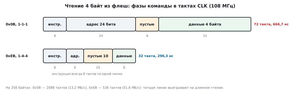
41в.2 A command: phases and lines
Every access to the flash is a command made of phases (RM0385, 14.3.3): instruction (8 bits), address (8–32 bits), alternate bytes, dummy clocks, data. The number of lines is set separately for each phase: IMODE for the instruction, ADMODE for the address, DMODE for the data — 00 no phase, 01 one line, 10 two, 11 four. Dummy clocks are the DCYC field, 0–31. All of this lives in the QUADSPI_CCR register together with the instruction code and the FMODE mode.
A notation like "1-4-4" means: the instruction on one line, the address and the data
on four. The 0xEB command of the N25Q128A flash is exactly that, with 10 dummy
clocks (the BSP driver, N25Q128A_DUMMY_CYCLES_READ_QUAD). Clocks per
read, 24-bit address, QUADSPI at 108 MHz (216 MHz / 2, as in the BSP):
| Command | Lines | Dummy | 4 bytes | 256 bytes | Throughput |
|---|---|---|---|---|---|
| 0x0B fast read | 1-1-1 | 8 | 72 clocks, 666.7 ns | 2088 clocks, 19.33 µs | 13.2 MB/s |
| 0xEB | 1-4-4 | 10 | 32 clocks, 296.3 ns | 536 clocks, 4.96 µs | 51.6 MB/s |
On a long read four lines give almost four times more (the limit is 54 MB/s). On a single word the gain is twofold: the instruction still goes over one line for 8 clocks, and the dummy clocks do not go away. So code that jumps around the flash gains less from Quad-SPI than sequential reading does — and that is why the cache and read-ahead matter (41в.4).
41в.3 Register-level setup
The STM32746G-Discovery has a 16 MB N25Q128A flash: nCS — PB6, CLK — PB2, IO0–IO3 — PD11, PD12, PE2, PD13 (AF9 and AF10). The BSP numbers in the registers:
- CR: PRESCALER 1 — 216 / (1 + 1) = 108 MHz; FIFO threshold 4 bytes; SSHIFT — sampling half a clock later (for delays on the board).
- DCR: FSIZE 23 — bytes 2^(23 + 1) = 16 MB; CSHT 5 — nCS high for at least 6 clocks between commands (the BSP comment says "at least 50 ns").
- CCR for mapping: FMODE 11, 0xEB, 1-4-4, 24 bits, DCYC 10 — the value 0x0F28 2DEB.
void qspi_init(void)                    /* выводы PB2, PB6, PD11–13, PE2 — AF9/AF10, их настраивает CubeMX */
{
    RCC->AHB3ENR |= RCC_AHB3ENR_QSPIEN;
    QUADSPI->CR  = (1u << QUADSPI_CR_PRESCALER_Pos)     /* 216 / (1 + 1) = 108 МГц */
                 | (3u << QUADSPI_CR_FTHRES_Pos)        /* порог FIFO — 4 байта */
                 | QUADSPI_CR_SSHIFT;                   /* выборка на полтакта позже */
    QUADSPI->DCR = (23u << QUADSPI_DCR_FSIZE_Pos)       /* 2^(23 + 1) = 16 МБ */
                 | (5u << QUADSPI_DCR_CSHT_Pos);        /* nCS между командами — 6 тактов */
    QUADSPI->CR |= QUADSPI_CR_EN;
}
After CCR is written with FMODE = 11, the flash is an array at 0x9000 0000. The function
qspi_read_word(offset) from the example file compiles under armclang to a single load
instruction:
qspi_read_word:  MOV  r1,#0x90000000
                 LDR  r0,[r0,r1]
No exchange code at all: the controller sends the 0xEB command itself as soon as the CPU or DMA reads the window.
41в.4 Memory mapping: what you can and cannot do
RM0385 (14.3.7 and 14.3.11) sets the rules:
- in this mode — read only; erasing and writing are done in indirect mode;
- accessing the window before the controller is configured and enabled is forbidden;
- an address beyond FSIZE but inside the 256 MB window is a bus error: on the core a BusFault (or a HardFault if BusFault is not enabled), on DMA a transfer error;
- the window is no larger than 256 MB, even if the flash is larger;
- the controller reads ahead: the FIFO serves as a prefetch buffer, and on sequential reads the next byte is already there — this is what XIP support is.
The price of prefetching: by default the controller does not stop it and keeps
nCS low even if there have been no accesses for a long time, and a flash with nCS low
draws more current. The TCEN bit in CR and the timeout in LPTR release nCS after
a pause. And while prefetching is going on, the BUSY flag does not drop — while the CCR fields can
be changed only with BUSY = 0. You leave mapping with the ABORT bit: it
clears itself when the abort has finished (the qspi_leave_mapped function).
41в.5 Erasing and writing
The N25Q128A flash: 256-byte page, 4 KB subsector, 64 KB sector — 65536 pages, 4096 subsectors, 256 sectors. A 1 MB firmware image is 4096 pages and 256 subsectors (or 16 sectors). The order for each chunk:
- Leave mapping (ABORT).
- Command 0x06 — write enable (
qspi_write_enable: only the instruction, no address and no data). - Subsector erase 0x20 with an address.
- Wait until the flash finishes: automatic polling of status 0x05 with a mask
on the WIP bit (
qspi_wait_ready). The CPU does not read the status in a loop — the controller itself sends 0x05 and raises the SMF flag when WIP = 0. - 0x06 again and a page program (256 bytes per command).
- Wait for WIP again.
- Restore mapping.
How long to wait: the BSP driver allows up to 800 ms for a subsector erase, up to 3 s for a sector, up to 250 s for the whole chip.
The functions that do this cannot live in the same flash: while an indirect
command is running, the 0x9000 0000 window does not exist. They are kept in the internal Flash or
in RAM. And on the F7, after a write you must invalidate the D-cache for the changed range
(SCB_InvalidateDCache_by_Addr, section 11б): otherwise the core will read
stale data from the cache.
41в.6 Code in external flash
According to the Cortex-M7 memory map (DUI 0646B, tables 2-11 and 2-12) the region 0x8000 0000–0x9FFF FFFF is External RAM: type Normal, executable, write-through cache. So the QUADSPI window at 0x9000 0000 is fine for code without MPU setup, and the instruction cache hides the latency of the first access.
What you need to do:
- in the linker script (section 11) — a region at 0x9000 0000 of 16 MB and a section for code or constants (images, fonts, tables), and mark the functions with an attribute for that section;
- for the programmer — an algorithm for writing the external flash: in the Keil F7 pack for
this board there is
STM32F7xx_QSPI_Disco.FLMwith start 0x9000 0000 and size 16 MB; STM32CubeProgrammer has its own external loader; - at startup —
qspi_initand mapping before the first call to code in the flash: the setup itself must live in the internal Flash.
A convenient split: code that startup depends on (startup code, clock and QUADSPI setup, firmware update) goes in the internal Flash; large data and rarely called code go outside.
41в.7 Pitfalls
- Accessing the window before setup. A debugger that opened a memory window at
0x9000 0000, or a C++ constructor that read a constant from the external
flash before
qspi_init— and you get a BusFault or HardFault. - FSIZE smaller than the flash. A read beyond FSIZE is a bus error, not zero; set FSIZE to the flash size: 16 MB means 23.
- Dummy clocks do not match the flash. DCYC must match the number of dummy clocks the flash is configured for (on the N25Q128A, a field in its configuration register). Otherwise the data is shifted by half a byte or a byte: "everything reads, but the wrong thing".
- Erasing from code in the external flash. While an indirect command is running, the window does not exist, and the CPU cannot fetch the next instruction. The write code goes in the internal Flash or RAM.
- Stale data after a write. The F7 cache holds lines of the external flash; after erasing and writing, invalidate the D-cache for the changed range.
- SSHIFT in DDR. In double data rate mode (DDRM = 1) the sampling shift is not supported: the SSHIFT bit must be cleared (RM0385, 14.3.9).
- nCS low forever. Prefetching keeps the flash selected; where current matters, use TCEN and the timeout.
41в.8 Summary
- Three modes: indirect, automatic status polling, and mapping at 0x9000 0000 (read-only, a window of up to 256 MB).
- A command consists of instruction, address, dummy-clock and data phases; the lines for each are set separately. 0xEB "1-4-4" with 10 dummy clocks: 32 clocks per word, 296 ns at 108 MHz; throughput up to 51.6 MB/s on 256 bytes.
- The N25Q128A on the 746G-Discovery: FSIZE 23, PRESCALER 1, CSHT 5, CCR 0x0F28 2DEB.
- Erasing and writing in indirect mode, waiting by automatic polling of WIP; the write code must not be in the external flash; after a write, invalidate the D-cache.
- On a Cortex-M7 the 0x9000 0000 window is Normal and executable: code can be kept outside without the MPU; the programmer needs an external flash algorithm.
Full sources
qspi41c.c — register-level Quad-SPI on the STM32F746 with an N25Q128A flash.
/* 41в: Quad-SPI по регистрам на STM32F746 — флеш N25Q128A (16 МБ), как у STM32746G-Discovery.
   Собирается armclang: -DSTM32F746xx. */
#include <stdint.h>

/* поля QUADSPI_CCR — RM0385, 14.5.6 */
#define CCR(fmode, dmode, dcyc, adsize, admode, imode, inst) \
    (((uint32_t)(fmode) << QUADSPI_CCR_FMODE_Pos) | ((uint32_t)(dmode) << QUADSPI_CCR_DMODE_Pos) | \
     ((uint32_t)(dcyc) << QUADSPI_CCR_DCYC_Pos) | ((uint32_t)(adsize) << QUADSPI_CCR_ADSIZE_Pos) | \
     ((uint32_t)(admode) << QUADSPI_CCR_ADMODE_Pos) | ((uint32_t)(imode) << QUADSPI_CCR_IMODE_Pos) | (inst))

enum { F_WRITE = 0, F_READ = 1, F_POLL = 2, F_MAPPED = 3 };        /* FMODE */
enum { L_NONE = 0, L_1 = 1, L_2 = 2, L_4 = 3 };                     /* IMODE, ADMODE, DMODE */
enum { A_24 = 2 };                                                  /* ADSIZE */

#define CCR_MAPPED  CCR(F_MAPPED, L_4, 10, A_24, L_4, L_1, 0xEB)   /* 0xEB: 1-4-4, 10 пустых */
_Static_assert(CCR_MAPPED == 0x0F282DEBu, "CCR режима отображения");
_Static_assert(QSPI_BASE == 0x90000000u && QSPI_R_BASE == 0xA0001000u, "окно флеш и регистры");

static void qspi_wait_idle(void)
{
    while (QUADSPI->SR & QUADSPI_SR_BUSY) {
    }
}

void qspi_init(void)                    /* выводы PB2, PB6, PD11–13, PE2 — AF9/AF10, их настраивает CubeMX */
{
    RCC->AHB3ENR |= RCC_AHB3ENR_QSPIEN;
    QUADSPI->CR  = (1u << QUADSPI_CR_PRESCALER_Pos)     /* 216 / (1 + 1) = 108 МГц */
                 | (3u << QUADSPI_CR_FTHRES_Pos)        /* порог FIFO — 4 байта */
                 | QUADSPI_CR_SSHIFT;                   /* выборка на полтакта позже */
    QUADSPI->DCR = (23u << QUADSPI_DCR_FSIZE_Pos)       /* 2^(23 + 1) = 16 МБ */
                 | (5u << QUADSPI_DCR_CSHT_Pos);        /* nCS между командами — 6 тактов */
    QUADSPI->CR |= QUADSPI_CR_EN;
}

/* команда без адреса и данных: 0x06 — разрешить запись */
void qspi_write_enable(void)
{
    qspi_wait_idle();
    QUADSPI->CCR = CCR(F_WRITE, L_NONE, 0, 0, L_NONE, L_1, 0x06);
    qspi_wait_idle();
}

/* ждать конца стирания или записи: контроллер сам читает статус 0x05, пока бит WIP не станет 0 */
void qspi_wait_ready(void)
{
    qspi_wait_idle();
    QUADSPI->DLR   = 0;                  /* один байт статуса */
    QUADSPI->PSMKR = 0x01;               /* маска: WIP */
    QUADSPI->PSMAR = 0x00;               /* ждём WIP = 0 */
    QUADSPI->PIR   = 16;                 /* пауза между опросами, тактов */
    QUADSPI->CR   |= QUADSPI_CR_APMS;    /* остановиться при совпадении */
    QUADSPI->CCR   = CCR(F_POLL, L_1, 0, 0, L_NONE, L_1, 0x05);
    while (!(QUADSPI->SR & QUADSPI_SR_SMF)) {
    }
    QUADSPI->FCR = QUADSPI_FCR_CSMF;
}

/* включить отображение: флеш видна с 0x90000000, только чтение */
void qspi_memory_mapped(void)
{
    qspi_wait_idle();
    QUADSPI->CCR = CCR_MAPPED;
}

/* выйти из отображения перед стиранием и записью: BUSY держится из-за упреждающего чтения */
void qspi_leave_mapped(void)
{
    QUADSPI->CR |= QUADSPI_CR_ABORT;
    while (QUADSPI->CR & QUADSPI_CR_ABORT) {
    }
}

uint32_t qspi_read_word(uint32_t offset)
{
    return *(volatile const uint32_t *)(QSPI_BASE + offset);
}
Next: section 42 "The FatFS file system" — how to store files on top of external memory.