 Embedded HandbookApps
166. Resistors in detail: TCR, pulse load, shunt, battery divider
Ohm's law, the standard value series, marking and package power are covered in section 49, the divider and RC circuits in section 50, bus pull-ups in 95, pin protection with a resistor in 62. This section covers where a resistor lets you down when the circuit is already "correct": it changes with temperature, it heats up not only from DC current, it measures current with an error caused by the solder, and it quietly drains the battery.
All numbers below come from ngspice models with the stated parameters.
Terms used in the documentation
Term Meaning thick film / thin film resistor resistor with a thick / thin resistive film temperature coefficient of resistance (TCR) how much the resistance changes per degree ppm/°C parts per million per degree ratio tracking how closely a pair of resistors drifts together pulse load / single pulse energy short-pulse load / energy of one pulse inrush current current surge at power-on current sense resistor (shunt) resistor used to measure current Kelvin (4-wire) connection separate sense leads taken from the resistor body limiting element voltage maximum working voltage derating running a part below its rated load high-side / low-side switch switch on the supply side / ground side leakage current small current through an "off" path
166.1 Types of resistors
| Type | TCR | Where it is used |
|---|---|---|
| thick-film chip | ±100 ppm/°C or worse | almost everywhere: pull-ups, LEDs, non-precision dividers |
| thin-film chip | ±25 ppm/°C or better | dividers for the ADC, amplifier feedback |
| metal-film through-hole | in between | prototypes, low-power power circuits |
| wirewound | very low | precision and high-power circuits |
| metal shunt | low, specified | current measurement |
TCR is how many parts per million of its resistance a resistor loses or gains per degree. ±100 ppm/°C over 60 °C of heating is 0.6 %, more than the tolerance of a precision resistor. A thick-film resistor is also noisier than a thin-film one when current flows through it: on top of thermal noise (section 165.2) it adds excess noise proportional to the voltage across the resistor (in the documentation, the noise index, µV/V). Thin-film and wirewound resistors have almost none of it.
166.2 TCR and divider drift
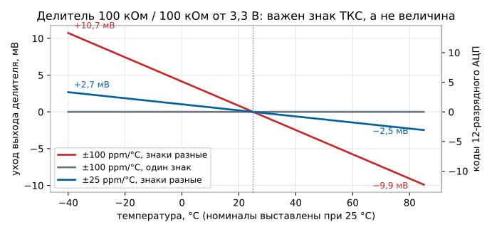
A 100 kΩ / 100 kΩ divider from 3.3 V into an ADC input, values exactly trimmed at 25 °C. The worst case is when the upper and lower resistors have TCRs of the same magnitude but opposite sign:
| Resistors | 85 °C | −40 °C |
|---|---|---|
| thick-film ±100 ppm/°C, opposite signs | −9.9 mV (12.3 codes) | +10.7 mV (13.3 codes) |
| thick-film, same sign | 0.0 mV | 0.0 mV |
| thin-film ±25 ppm/°C, opposite signs | −2.5 mV (3.1 codes) | +2.7 mV (3.3 codes) |
What matters to a divider is not the resistance but the ratio: if both resistors drift the same way, the output stays put. That is why a precision divider is built from resistors of the same batch and the same type, or you take a ready-made "two in one package" network whose ratio drift is specified. A drift of 0.60 % of reading at 85 °C cannot be removed by calibration at room temperature (section 164.5).
166.3 Pulse: the energy does not depend on the resistance
A 1000 µF capacitor charges from 24 V through a resistor at power-on. It is tempting to fit a larger resistor to "limit the current":
| Resistor | Peak current | Time constant | Energy in the resistor |
|---|---|---|---|
| 1 Ω | 24 A | 1 ms | 0.288 J |
| 10 Ω | 2.4 A | 10 ms | 0.288 J |
| 100 Ω | 0.24 A | 100 ms | 0.288 J |
The peak current drops a hundredfold, but the energy in the resistor stays at
0.288 J — exactly what is stored in the charged capacitor:
C · U² / 2. More resistance means the same energy over a longer time.
Two conclusions follow. The rated power of the package tells you nothing
here — the average power after charging is zero; you choose the resistor from
the pulse load graph in the documentation (single pulse energy
or allowed power for a given duration). And if the charge
repeats at frequency f, the resistor sees an average power of
E · f: the same 0.288 J ten times per second is 2.88 W.
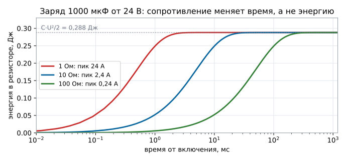
Charging to 99 % takes 4.6 time constants: 4.6 ms, 46 ms and 0.46 s.
166.4 Shunt: sense on the resistor body, not on the pads
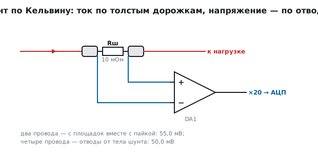
A current of 5 A through a 10 mΩ shunt gives 50 mV. The solder and trace up to the pads add 0.5 mΩ on each side. Where to take the voltage from:
| Connection | Voltage | Error |
|---|---|---|
| two wires: from the pads, in the current path | 55.0 mV | +10 % |
| four wires: sense leads from the shunt body | 50.0 mV | 0 % |
A milliohm of solder on a 10 mΩ shunt is a ten percent error, and it also drifts with temperature: copper trace has a TCR of about +3900 ppm/°C. With a four-wire connection the current flows through wide traces, while separate thin sense traces, carrying no current, go to the amplifier, and they pick up the voltage as close to the resistor body as possible. A four-terminal shunt has dedicated sense terminals for this. On a two-terminal shunt the sense trace leaves from the inner edge of the pad, right under the shunt terminal, so the solder that carries the current hardly enters the measurement. After a ×20 gain this is 1.00 V instead of 1.10 V.
Power: I² · R = 5² · 10 mΩ = 0.25 W — choose a shunt rated 0.5 W or
more: the rated package power is given at a moderate temperature, as
the board heats up the allowed power drops, and the shunt itself drifts as it heats.
166.5 Battery divider: leakage and the switch
A 4.2 V lithium cell through a divider into an ADC input (MCU supply 3.3 V). The divider loads the battery all the time unless you disconnect it. Three options:
| Option | Idle current | ADC pin when idle | Current during measurement |
|---|---|---|---|
| 1 MΩ / 1 MΩ, no switch | 2.1 µA | 2.10 V | 2.1 µA |
| 100 kΩ / 100 kΩ, low-side N switch | 3.9 µA | 3.81 V | 21 µA |
| 100 kΩ / 100 kΩ, high-side P switch | 12 pA | 0.00 V | 63 µA |
Without a switch, 2.1 µA over a year is 18.4 mAh: nothing for a rechargeable cell, noticeable for a coin cell. A high-value divider also needs a capacitor at the ADC input (section 50.6).
A low-side switch is a mistake. When the switch is off it disconnects the bottom of the divider, and the upper resistor pulls the pin up toward the battery. The pin rises to 3.81 V, above the MCU supply, and a 3.9 µA current flows through the pin's protection diode into the supply rail — more than with no switch at all. This is the injection current from section 62 and a violation of the pin's absolute maximum voltage.
A high-side P switch disconnects the divider from the battery: when idle the pin is at ground, and the leakage is only the off-state current of the transistor (12 pA in the model). The gate is pulled up to the battery by a 100 kΩ resistor and is turned on by an N switch driven from an MCU pin; during the measurement the gate pull-up current is added: 21 + 42 = 63 µA. A 10 ms measurement once a minute averages 10.5 nA.
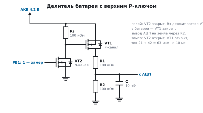
Is 10 ms enough? The divider resistance seen from the pin is 50 kΩ; with a 10 nF capacitor at the input the time constant is 0.5 ms, so 10 ms is 20 time constants and the output has settled.
166.6 Working voltage
Besides power, a resistor has a maximum working voltage, and for small packages it is a few tens of volts. A mains divider is not built from a single resistor: the peak of 230 V · √2 = 325 V is shared across several resistors in series, three resistors give 108 V each. As a bonus, a single short across one resistor does not put the full voltage on the low side. Take the limit from the documentation of the series: it grows with the package size. And do not count only the 325 V peak: mains surges reach kilovolts, so use resistors rated for high voltage and keep the clearances on the board.
166.7 Pitfalls
ADC readings drift with temperature although the reference is stable. The divider is built from resistors of different types or with TCRs of opposite sign; use one batch or a resistor network.
The precharge resistor burned out although its power rating was fine. It was sized by average power, but it receives the capacitor's charge energy within milliseconds — choose it by pulse load.
The shunt current reads about ten percent high and drifts. The voltage is taken from the pads together with the solder — use a four-wire connection.
The battery drains faster than calculated while the device is off. The divider loads the battery all the time or is switched off with a low-side switch.
The ADC pin is "live" while the divider is switched off. Low-side switch: the upper resistor pulls the pin toward the battery, above the MCU supply — use a high-side switch.
The battery reading is wrong right after the switch turns on. You did not wait for it to settle: 50 kΩ and the input capacitance form a time constant; wait 5–10 τ.
166.8 Summary
- TCRs of ±100 ppm/°C with opposite signs shift a 100 kΩ / 100 kΩ divider by −9.9 mV at 85 °C and +10.7 mV at −40 °C; same sign gives 0; thin-film ±25 gives −2.5 mV.
- Charging 1000 µF from 24 V puts 0.288 J into the resistor at 1, 10 and 100 Ω; only the peak current changes: 24 A, 2.4 A, 0.24 A.
- 1 mΩ of solder on a 10 mΩ shunt gives +10 %: 55.0 mV instead of 50.0; use a four-wire connection.
- Disconnect a battery divider with a high-side P switch: 12 pA idle and 0.00 V on the pin; a low-side switch gives 3.81 V on the pin and 3.9 µA into the supply rail.
Next: section 167 "Capacitors".