 Embedded HandbookApps
164. Real op-amp parameters: input bias current, supply noise, rail-to-rail
Section 56 covered the essentials: offset voltage, bandwidth, slew rate. This section covers what sits a few lines lower in the documentation and what people remember once the board is already assembled: input bias current and its compensation, supply noise, which is barely rejected at high frequencies, the offset step of a rail-to-rail input, and an output that is "rail-to-rail" only without a load. At the end everything comes together in one error budget for the channel — in ADC codes.
All numbers below come from an ngspice model with explicitly set parameters of a typical low-cost part: input bias current 100 nA, power supply rejection 100 dB rolling off from 10 Hz, a 1 mV offset jump when the input pairs switch over at 2.2 V, and an output that gets within 10 mV of the rail plus another 50 mV for every milliampere of load (50 Ω in series). A specific part has its own figures, but the behaviour is like this.
Terms used in the documentation
Term Meaning input bias current (Ib) current flowing into the inputs input offset current (Ios) difference between the two input currents bias current compensation balancing the resistances seen by both inputs power supply rejection ratio (PSRR) how well supply noise is suppressed supply decoupling / RC filter filtering the amplifier supply rail-to-rail input input range from one rail to the other input pair crossover handover between the two input pairs output voltage swing how close the output gets to the rails output current current the output can source or sink input offset voltage drift (TCVos) change of offset voltage with temperature error budget all error sources of a channel added up worst case / root sum square (RSS) straight sum / square root of the sum of squares typical / maximum value usual value / guaranteed limit test conditions conditions under which a parameter is measured
164.1 Input bias current and the compensating resistor
Current flows into the inputs of an amplifier with a bipolar input — say 100 nA. A non-inverting ×11 (Rf 100 kΩ, Rg 10 kΩ) around the midpoint of 1.65 V:
| Source resistance at "+" | Output error |
|---|---|
| 0 Ω | +10.00 mV |
| 100 kΩ | −99.99 mV |
| 9.1 kΩ ≈ Rf ∥ Rg | −0.01 mV |
With zero source resistance the error comes from the current of the inverting
input flowing through Rf: 100 nA · 100 kΩ = 10 mV. With a
100 kΩ source the "+" current makes a voltage drop across it, and this drop is amplified 11 times.
If the resistance at "+" is made equal to Rf ∥ Rg — here 9.09 kΩ,
a 9.1 kΩ is used — the two drops subtract, and the error falls 1000 times:
from 10 mV to hundredths of a millivolt.
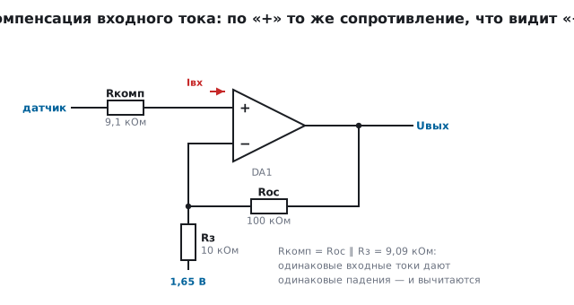
Compensation does not remove the input offset current. Equal currents subtract, but the difference does not. Say 110 nA flows into "+" and 90 nA into "−": the same circuit with 9.1 kΩ gives −2.01 mV — that is the 20 nA difference across Rf. The documentation lists it on a separate line, and for a compensated circuit the calculation uses this value, not the input bias current itself.
FET input. The input bias current is a few picoamperes at 25 °C, but that is mostly leakage of the input protection diodes, and it doubles roughly every 10 °C: 1 pA at 25 °C becomes 64 pA at 85 °C. On a 10 MΩ source that is already 0.64 mV — for sensors with a high internal resistance the "at 25 °C" line guarantees nothing.
One more consequence of a single supply: the experiment is set up around the midpoint of 1.65 V, because with a 0 V reference the input bias current would pull the input below ground, and the output would hit the rail.
164.2 Supply noise and frequency
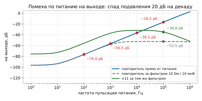
Power supply rejection is huge at low frequency, but it falls by 20 dB per decade. For the follower in the model, this much reaches the output:
| Ripple frequency | At the output |
|---|---|
| 100 Hz | −76.4 dB |
| 1 kHz | −56.5 dB |
| 10 kHz | −36.5 dB |
| 100 kHz | −16.5 dB |
The numbers are 3.5 dB higher than rejection alone gives (−80 dB at 100 Hz): in the model the noise also passes through the output stage, which is referred to the supply midpoint — that adds another half of the first path. Real amplifiers can behave this way too, so trust the rejection graph in the documentation, not a single figure.
A switching regulator works right in the hundreds of kilohertz: its 50 mV ripple at 100 kHz reaches the amplifier output as 7.5 mV — several codes of a 12-bit ADC.
Supply filter. A 10 Ω resistor and a 10 µF capacitor in front of the amplifier supply pin — a corner at 1.59 kHz. At 100 kHz it adds another 36 dB: the follower gets −52.5 dB, and the same 50 mV becomes 0.12 mV. The drop across 10 Ω at a supply current of 1 mA is 10 mV, which does not bother the amplifier; a 100 nF ceramic capacitor is still placed right at the pin — the filter works at kilohertz, the ceramic at megahertz.
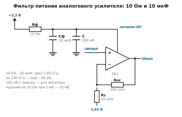
A circuit with gain amplifies the noise too. Power supply rejection in the documentation is referred to the input — the noise adds to the offset and goes through the circuit with its gain. A non-inverting ×11 behind the same filter: at 1 kHz −37.1 dB — exactly 20.8 dB (×11) more than the follower; at 100 kHz −34.8 dB, 0.91 mV. This is less than 11 × 0.12 mV, because the bandwidth of ×11 with 1 MHz is 91 kHz, and at 100 kHz the gain is already rolling off.
164.3 Rail-to-rail input: the offset step
For the input to work from rail to rail, there are two input pairs inside: one works near the bottom rail, the other near the top. Somewhere around the upper third of the range operation is handed over from one to the other, and the offset voltage changes in a jump.
The model is a follower: the error is 0 mV up to 1 V, 0.50 mV right at the threshold of 2.2 V and 1.00 mV above it. For a follower this is a trifle, but a non-inverting ×50 turns the same step into 50 mV at the output — in the middle of the scale.
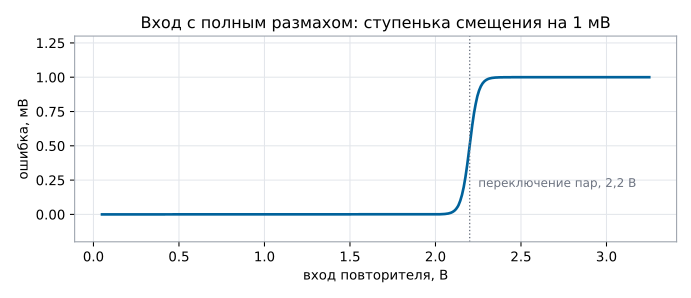
The cure is a choice: a part with a single input pair and an internal charge pump, or a circuit operating point that does not cross the threshold.
164.4 Rail-to-rail output under load
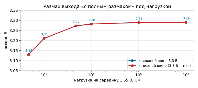
The "rail-to-rail" output swing in the documentation is given at a specified load. A follower pulls towards 3.3 V and towards zero, with the load returned to the midpoint of 1.65 V:
| Load | Top | Bottom |
|---|---|---|
| 1 MΩ | 3.29 V | 0.01 V |
| 100 kΩ | 3.29 V | 0.01 V |
| 10 kΩ | 3.28 V | 0.02 V |
| 4.7 kΩ | 3.27 V | 0.03 V |
| 1 kΩ | 3.21 V | 0.09 V |
| 470 Ω | 3.13 V | 0.17 V |
With a 1 kΩ load the top of the ADC scale loses 0.09 V — about 110 codes of a 12-bit ADC. If the output drives something low-impedance, the margin at the rails is calculated from the load current, not from the first row of the table.
164.5 The channel error budget
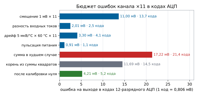
Let us put everything into one channel: a sensor through the compensated ×11 from 164.1 into a 12-bit ADC with a 3.3 V reference, one code is 0.806 mV. We take the maximum values from the documentation: offset 1 mV, offset drift 5 µV/°C, input offset current 20 nA. The board works up to 85 °C, powered from a switching regulator with 50 mV ripple at 100 kHz through the 10 Ω / 10 µF filter from 164.2.
| Source | How calculated | At the output | Codes |
|---|---|---|---|
| offset | 1 mV × 11 | 11.00 mV | 13.7 |
| input offset current | model, 164.1 | 2.01 mV | 2.5 |
| offset drift | 5 µV/°C × 60 °C × 11 | 3.30 mV | 4.1 |
| supply ripple | model, 164.2 | 0.91 mV | 1.1 |
| sum | worst case | 17.22 mV | 21.4 |
| root sum square | sources are independent | 11.69 mV | 14.5 |
The sum is a guarantee: this is what you get on the worst board, if all sources go the same way. The root sum square is an estimate for most boards: independent sources rarely all go the worst way at the same time.
The share matters more than the total. Three quarters of the error comes from the constant terms: offset and input offset current, 13.01 mV. A zero calibration at 25 °C removes them — measuring the output with zero signal and subtracting it in software. What remains is drift and ripple: 4.21 mV, 5.2 codes, and 3.30 mV of that is drift. From here on it pays more to look for a part with lower drift than to filter the supply even harder.
All of these are zero errors: they are the same at any signal. At full scale a gain error is added to them. The gain is set by resistors: with 1 % tolerance on each, in the worst case it is between 10.80 and 11.20, that is ±1.8 %, and with a 3 V signal at the output this is up to 55 mV — 68 codes, three times the whole table. The ADC reference errs the same way — as a percentage of full scale — and the ADC itself adds its own total error: for the F103 and F407, up to ±5 codes per the datasheet. A zero calibration removes the offset, a two-point calibration also removes the gain error; after it, drift and the ADC's own error remain.
Ripple is an AC quantity: averaging many samples reduces it, as long as the sampling rate is not a multiple of the ripple frequency. Averaging does not touch the constant terms.
164.6 How to read the parameter table
- Typical and maximum. Designing to the typical value means that half of the boards will come out worse. Maximum values are what the manufacturer guarantees.
- Conditions. Each line is measured at its own supply, load and temperature; the output swing at 10 kΩ says nothing about 1 kΩ.
- Over temperature. Offset, input bias current and offset current change; for a FET input the bias current grows quickly with heat — compare the graphs over temperature, not the line at 25 °C.
- Graphs matter more than the table for frequency parameters: power supply rejection in the table is given at DC, but it has to work at hundreds of kilohertz.
- Referred to the input. Offset, drift, supply noise and noise in the documentation are given at the input; the circuit's noise gain carries them to the output — for a non-inverting ×11 it is 11, for an inverting ×−10 it is also 11.
164.7 Pitfalls
The error grows with sensor resistance, while the part's offset is small.
The input bias current across the source resistance; make the resistance at "+" equal to
Rf ∥ Rg.
The compensating resistor is in place, but the error is still millivolts. The calculation used the input bias current, but what remains is the input offset current across Rf.
The switching regulator frequency is visible at the output. Power supply rejection at hundreds of kilohertz is almost zero — a supply filter.
A jump of tens of millivolts appeared in the middle of the scale. The input pair crossover of a rail-to-rail input, amplified by the circuit.
The top ADC codes are never reached. The output swing is specified without a load or at 10 kΩ, while the circuit is loaded with a kilohm.
Zero was calibrated at room temperature, but when warm the zero moved again. Offset drift cannot be calibrated at a single point; after calibration it is the largest term in the budget.
When warm, the readings drift more than the table promises. The calculation used typical values at 25 °C.
164.8 Summary
- Input bias current of 100 nA at ×11: a 100 kΩ source gives −99.99 mV, a zero one +10.00 mV; a resistance at "+" equal to Rf ∥ Rg = 9.09 kΩ leaves −0.01 mV. Compensation does not remove the 20 nA input offset current: −2.01 mV.
- Power supply rejection falls by 20 dB per decade: the follower has −76.4 dB at 100 Hz and −16.5 dB at 100 kHz — 50 mV of ripple gives 7.5 mV; a 10 Ω / 10 µF filter leaves 0.12 mV, and ×11 behind it 0.91 mV.
- Input pair crossover gives a 1.00 mV offset step; at ×50 that is 50 mV.
- A "rail-to-rail" output on 1 kΩ reaches 3.21 V and 0.09 V, on 470 Ω only 3.13 V and 0.17 V.
- Budget of the ×11 channel: 17.22 mV worst case (21.4 codes), 11.69 mV by root sum square; a zero calibration leaves 4.21 mV — mostly drift. At full scale the gain error is the largest: 1 % resistors give up to 55 mV, 68 codes — a two-point calibration removes it.
Next: section 165 "Noise".