 Embedded HandbookApps
11в. Read protection on the F1: why level 1 does not save the firmware
Section 11 (subsection 11.6) introduced the option bytes and the RDP read protection:
the value 0xA5 on the F1 means "no protection", any other means first-level
protection, after which the debugger cannot read Flash, and it can only be removed
together with erasing the whole memory. For debugging this is enough. For a product
that will go to strangers, the question is different: how much does the first level
hinder someone who holds the board in their hands and wants to pull the firmware out.
Here is an honest answer for the F1. What the first level promises and honestly delivers; where its weakness lies specifically on the F1 (the principle was publicly described long ago); and what follows from this for a product. The tone of the section is defensive: it is about choosing the chip and the measures, not about removing someone else's protection. There is no ready-made extraction tool here.
Prerequisites: section 11 (memory map, option bytes 11.6), section 48 (bootloader protection 48.9), image signing (48а), and also chips with strong protection — STM32U5 and TrustZone (2б, 2е).
Terms used in the documentation
Term Meaning read protection level (RDP level) the level of read-out protection vector fetch reading the handler address from the vector table exception stacking pushing the exception frame onto the stack threat model who the attacker is and what they can do one-time programmable (OTP) memory that can be written only once device unique ID (UID) the factory serial number of the die
11в.1 What level 1 promises
Read protection lives in one option byte — RDP. On the F1 protection is
switched off by the single value 0xA5; any other value enables the first level.
When it is enabled, the F103 documentation (RM0008, the section on embedded Flash)
promises exactly the following:
- the debugger still connects — it sees the core, the registers, the peripherals;
- but reading, erasing and writing main Flash through the debugger, and also when booting from RAM or system memory, are forbidden; an attempt to read gives a bus error;
- protection can only be removed by setting
RDPback to0xA5, and this is a full Flash erase: the code disappears before the protection is removed.
For development this is convenient: the board is not "locked forever", it is just that every
reflash after removing protection starts from a clean slate. An erased option
byte 0xFF gives a protected chip, not an open one — this is also from 11.6.
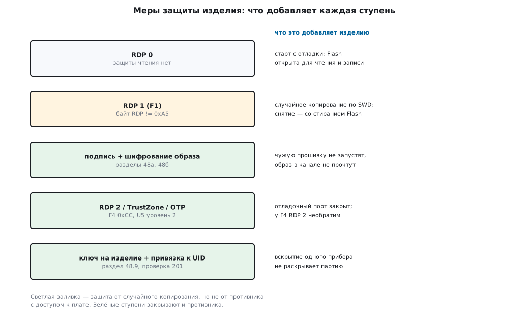
The ladder of product protection measures — from level zero to a unique key — is in the figure. The light steps add convenience and protection against casual copying, the green ones also stop an attacker with access to the board.
11в.2 Where the weakness lies on the F1
The promise "the debugger does not read Flash" holds for the normal data path: when the debugger asks for a byte at a Flash address directly, the memory controller answers with an error. The weakness of the F1 is that this is not the only path by which a value from Flash gets out.
The Cortex-M3 core itself reads Flash continuously in order to work: it fetches instructions from there and — on every exception entry — the handler address from the vector table (vector fetch). On the F1 two separate core buses lead to Flash (RM0008, the section on bus architecture): the ICode instruction bus for instruction fetch and the DCode data bus for literals and debugger access. First-level protection closes the path the debugger uses, but does not stop the core working — otherwise the chip simply would not start. And since the core reads Flash, the word read ends up in a register — the vector is loaded into the program counter — and the core registers are visible through the debug access that is not blocked.
That this is exactly what happens on exception entry is confirmed by the core documentation (Cortex-M3 Generic User Guide, the section on exception entry): "the processor performs a vector fetch that reads the exception handler start address from the vector table", and the state of the interrupted program — including the return address — is pushed onto the stack by the core (exception stacking). The core fetches the vector from Flash itself; the return address is the address of an instruction in Flash, not a word read from it.
This principle underlies the long-known, publicly described attack on RDP level 1 of the F1: by shifting the vector table base and triggering exceptions, through the debug interface that is not closed, one reads, one by one, the values that the core itself fetches from Flash. It has been assigned CVE-2020-8004, and a detailed analysis was published by the researchers. We do not give a step-by-step method or a ready-made tool here — what matters is the conclusion, not the recipe: on the F1 the first level is not designed for an attacker with physical access to the board.
On newer families this path is closed differently. On the F4 the first level is called "read protection enabled" in RM0090 (3.7.3), and full protection is given only by the second level, which disables debugging. On the U5 with TrustZone enabled in protected mode any debug access is flagged as an intrusion and closes access to memory in hardware (RM0456, the section on read protection). The F1 does not have these mechanisms.
11в.3 What each level gives: F1, F4, U5
Let us bring the levels of the three families into one table. The RDP byte values are from
the pack headers and reference manuals (RM0090 for the F4, RM0456 for the U5);
for the F1 — from the family header and its library.
| Series | Level | RDP byte | Debugger reads Flash | Removal | Irreversible |
|---|---|---|---|---|---|
| F1 | 0 | 0xA5 | yes | — | no |
| F1 | 1 | anything except 0xA5 | no | with full Flash erase | no |
| F4 | 0 | 0xAA | yes | — | no |
| F4 | 1 | anything except 0xAA and 0xCC | no | with full Flash erase | no |
| F4 | 2 | 0xCC | no debug | impossible | yes |
| U5 | 0 | 0xAA | yes | — | no |
| U5 | 0.5 | 0x55 (only with TrustZone) | only the non-secure part | via level 1 | no |
| U5 | 1 | anything except 0xAA, 0x55 and 0xCC | no | with erase; can be locked with the OEM1 key | no |
| U5 | 2 | 0xCC | no debug | only with an OEM2 key set in advance | without the OEM2 key — yes |
The main points of the table:
- The F1 has only one protection level above zero. A second one, with debug disabled, the F1 does not have — so there is no hardware protection against the principle described either.
- The F4 has two levels. The second (
0xCC) disables debugging and booting from system memory for ever: this is an irreversible operation, there is no back button. - The U5 has four grades (0, 0.5, 1, 2) and a link to TrustZone; the second level can be made removable only if the OEM2 key is provisioned in advance.
- In all three series the erased byte
0xFFfalls into the first level, not level zero: almost any value of the byte protects, "open" is one special value.
11в.4 Check: the core reads the vector from Flash itself
The principle from 11в.2 — "on exception entry the core reads the vector from Flash, and the value ends up in a register and on the stack" — can be shown on your own test firmware without touching anyone else's chip. This is a check of the documented behaviour of the core (vector fetch and frame stacking), not memory extraction: the firmware reads only its own vector table.
The firmware was built with arm-none-eabi-gcc for Cortex-M3 (176 bytes) and run
in QEMU on the stm32vldiscovery model (STM32F100). The vector table lies in
Flash; entry 11 is the SVC_Handler handler. The main function reads the vector
word, then raises an exception with the svc 0 instruction; the debugger (GDB over
the remote protocol) stops at the handler entry and looks at what
the core did on entry:
/* Голый обработчик: передаёт указатель кадра (MSP) в си-часть, не трогая его. */
__attribute__((naked)) void SVC_Handler(void)
{
    __asm volatile(
        "mrs r0, msp      \n"
        "b   svc_handler_c\n");
}
The C part of the handler receives the frame pointer and takes from it the return address — the very one the core pushed onto the stack on entry:
/* Си-часть обработчика: frame — кадр исключения на стеке; frame[6] — адрес
 * возврата (PC), который ядро само считало и положило на стек при входе. */
void svc_handler_c(uint32_t *frame)
{
    g_stacked_pc = frame[6];
    g_handler_addr = (uint32_t)SVC_Handler;
    g_svc_ran = 1u;
}
What the run showed (values from the run, addresses are in the Flash area
0x0800 ….):
| What we observe | Value |
|---|---|
word of vector 11 in Flash (address of SVC_Handler) |
0x0800 0045 |
| program counter PC at handler entry | 0x0800 0044 |
| return address pushed onto the stack by the core | 0x0800 008C |
| the handler actually ran | yes |
The word 0x0800 0045 is the address of SVC_Handler with the Thumb low bit; it got
into PC without that bit — 0x0800 0044. That is, the core itself read the word from
Flash and loaded it into a register (the program counter). The return address
0x0800 008C is the instruction in the main function right after svc; the core pushed
onto the stack an address pointing into Flash. The debugger asked Flash for neither
of them — the values were produced by the core itself on exception entry. It is exactly this normal
mechanism that is not closed by first-level protection on the F1.
The level table from 11в.3 was checked separately: a short calculation by the rules
of the documents gives that on the F1 the first level corresponds to 255 byte values out of 256,
on the F4 to 254 (except 0xAA and 0xCC), on the U5 to 253; the erased 0xFF in all three
falls into level 1. This matches the table of the section.
11в.5 What to do: a chip with strong protection
If a product must keep valuable firmware and will reach outsiders, protection is chosen by the threat model: casual copying by a neighbour on the shop floor or an attacker with a soldering iron and a debugger. Against the second, the first level of the F1 does not help — you need a chip where the debug path is closed in hardware.
- F4 with level 2. The byte
RDP = 0xCCdisables debugging, booting from system memory and any further change to the option bytes. This is reliable and irreversible: there is nothing to reflash such a board with after repair except the product's own working bootloader (section 48). Level 2 is put on the line deliberately, not in the first month of production (section 201 says the same). - U5 with TrustZone. Valuable code and keys are kept in the secure part, and read protection is raised to level 2 with regression by the OEM2 key — then debug access to memory is closed in hardware, while service keeps a controlled way back with the key. How this is set up in practice — sections 2б and 2е.
- OTP and one-time bits. Where there is no second level, part of the secret can be kept in one-time programmable memory: what is written once is not erased when protection is removed.
None of these measures makes extraction impossible against a laboratory with microprobes — but they raise the cost to a level at which it loses its point.
11в.6 What to do: do not rely on one byte
Chip protection is only one layer. Firmware is protected so that reading it gives the attacker nothing by itself, and substitution does not pass.
- Image signing (section 48а): the bootloader checks who made the firmware, and will not run someone else's. The root of trust is the first immutable stage.
- Image encryption (sections 48.9 and 48г): the firmware in the update channel and on disk is encrypted; reading Flash by itself does not give plaintext code.
- Do not keep secrets in plaintext in F1 Flash. An array of keys in the sources or in open Flash is not protection.
- A unique key per device, bound to the UID. One key for the whole batch means that opening one unit compromises them all. The key is derived from the device unique ID (UID) and a secret not stored in open Flash, and correct provisioning is checked in production (section 201).
So RDP level 1 on the F1 remains useful — as protection against casual copying and as hygiene — but the load-bearing layers for a valuable product are signing, encryption and a unique key, not one option byte.
11в.7 Pitfalls
- "We set RDP1 on the F1 — the firmware is in a safe." No: the first level on the F1 is protection against casual copying, not against an attacker with a debugger. Valuable code on the F1 without signing and encryption is open to whoever holds the board.
- A secret in open Flash "protected by RDP1". A value the core reads while working passes through registers and the stack. On the F1 keys and passwords must not be kept there — only in encrypted form or in OTP.
- Level 2 on the F4 "just to be sure" at the start of production.
RDP = 0xCCis irreversible: no debugging, no way back. Set early, it turns the very first defective board into an unrecoverable one. It is set as the last step and not at once. - Removing protection "without losses". Setting
RDPto the open value is always a full Flash erase. You cannot count on "I'll remove the protection and finish reading the firmware": by the time it is removed there is nothing left to read. - One key for the whole batch. Convenient in production, dangerous in the field: opening one unit exposes them all. The key is per device, bound to the UID.
- U5: level 2 without a provisioned OEM2 key. Without an OEM2 key written in advance, return from level 2 is impossible — just as irreversible as on the F4.
11в.8 Summary
- On the F1 read protection is one
RDPbyte and one protection level:0xA5is open, any other value (of 255 possible) is the first level. - The first level honestly closes the debugger's direct data path to Flash and is removed only by a full erase; but it does not block the normal fetch of vectors and instructions by the core, and the publicly described attack (CVE-2020-8004) is built on this.
- The QEMU model shows the core behaviour itself: on exception entry the vector
word
0x0800 0045from Flash ends up in the program counter (0x0800 0044), and the return address0x0800 008Con the stack. The core read the vector word from Flash itself, without a request from the debugger. - Conclusion for a product: RDP level 1 on the F1 is protection against casual copying, not against an attacker. Real protection needs chips with disableable debug: the F4 with level 2 (irreversible), the U5 with TrustZone and level 2, OTP for part of the secret.
- The load-bearing layers are signing (48а) and image encryption (48г), no secrets in open Flash, a unique per-device key bound to the UID and checked in production (201).
Full sources
vec_demo.c — test firmware: the core reads the vector from Flash itself on exception entry.
/* Раздел 11в: показ документированного поведения ядра Cortex-M3 на СВОЕЙ тестовой
 * прошивке (STM32F100, QEMU stm32vldiscovery). Прошивка демонстрирует, что при
 * входе в исключение ядро само читает адрес обработчика из таблицы векторов во
 * Flash и кладёт его в счётчик команд (регистр PC), а адрес возврата — на стек.
 * Это проверка штатного стекинга и выборки вектора, а не извлечение чужой памяти:
 * прошивка читает только собственную таблицу векторов и печатать содержимое чужого
 * кристалла не умеет. Собирается arm-none-eabi-gcc под cortex-m3. */

#include <stdint.h>

/* --- наблюдаемые величины: GDB читает их по именам --- */
volatile uint32_t g_vtor;          /* SCB->VTOR — где лежит таблица векторов   */
volatile uint32_t g_vec_svc;       /* слово Flash: вектор SVCall (запись 11)    */
volatile uint32_t g_vec_reset;     /* слово Flash: вектор сброса (запись 1)     */
volatile uint32_t g_handler_addr;  /* фактический адрес SVC_Handler             */
volatile uint32_t g_stacked_pc;    /* адрес возврата, который ядро положило на стек */
volatile uint32_t g_svc_ran;       /* 1 — обработчик отработал                  */

#define SCB_VTOR (*(volatile uint32_t *)0xE000ED08u)

extern uint32_t _estack;
void Reset_Handler(void);
void Default_Handler(void);
void SVC_Handler(void);

/* Таблица векторов во Flash: запись 1 — сброс, запись 11 — SVCall. */
__attribute__((section(".isr_vector"), used))
uint32_t *const isr_vector[16] = {
    (uint32_t *)&_estack,          /*  0  начальный указатель стека */
    (uint32_t *)Reset_Handler,     /*  1  сброс                     */
    (uint32_t *)Default_Handler,   /*  2  NMI                       */
    (uint32_t *)Default_Handler,   /*  3  HardFault                 */
    (uint32_t *)Default_Handler,   /*  4  MemManage                 */
    (uint32_t *)Default_Handler,   /*  5  BusFault                  */
    (uint32_t *)Default_Handler,   /*  6  UsageFault                */
    0, 0, 0, 0,                    /*  7..10 резерв                 */
    (uint32_t *)SVC_Handler,       /* 11  SVCall                    */
    (uint32_t *)Default_Handler,   /* 12  DebugMon                  */
    0,                             /* 13  резерв                    */
    (uint32_t *)Default_Handler,   /* 14  PendSV                    */
    (uint32_t *)Default_Handler,   /* 15  SysTick                   */
};

void Default_Handler(void)
{
    for (;;) {
    }
}

/* Си-часть обработчика: frame — кадр исключения на стеке; frame[6] — адрес
 * возврата (PC), который ядро само считало и положило на стек при входе. */
void svc_handler_c(uint32_t *frame)
{
    g_stacked_pc = frame[6];
    g_handler_addr = (uint32_t)SVC_Handler;
    g_svc_ran = 1u;
}

/* Голый обработчик: передаёт указатель кадра (MSP) в си-часть, не трогая его. */
__attribute__((naked)) void SVC_Handler(void)
{
    __asm volatile(
        "mrs r0, msp      \n"
        "b   svc_handler_c\n");
}

/* Точка остановки после возврата из исключения: здесь все g_* уже заполнены. */
__attribute__((noinline)) void checkpoint(void)
{
    __asm volatile("nop");
}

int main(void)
{
    /* Куда ядро смотрит за таблицей векторов и какие слова там лежат. */
    g_vtor = SCB_VTOR;
    g_vec_reset = ((volatile uint32_t *)g_vtor)[1];
    g_vec_svc = ((volatile uint32_t *)g_vtor)[11];

    /* Вызов исключения: ядро выберет вектор 11 из Flash и уйдёт в SVC_Handler. */
    __asm volatile("svc 0");

    /* После возврата: адрес обработчика, попавший в PC, = слово вектора во Flash
     * (без младшего бита Thumb); адрес возврата на стеке — тоже адрес Flash. */
    checkpoint();
    for (;;) {
    }
}

void Reset_Handler(void)
{
    main();
    for (;;) {
    }
}
Next: section 12 "Service blocks" — watchdog timers, hardware CRC and the real-time clock.