 Embedded HandbookApps
11б. Cache, TCM and memory domains on F7 and H7
Section 11 looked at the memory of the F103 and F407: one Flash, one or two RAMs, and whatever lies at an address is seen by both the core and DMA. In the Cortex-M7 of the F7 and H7, caches have appeared between the core and memory, next to the core there is its own fast TCM memory, and on the H7 the RAM is also spread over three domains. Code from the F407 ports over and works — until the first DMA buffer that suddenly receives old data or transmits zeros.
Sections 9 and 124 say it in two paragraphs: "clean the cache before transmitting, invalidate after receiving". Here — why, where a buffer may live and where it may not, and which trap remains even when the cache is maintained by the rules.
Prerequisites: reference manuals RM0385 (F74x/F75x) and RM0433 (H742/H743/H750), the F746 and H743 datasheets, the Cortex-M7 core manual (DUI 0646B). Cache behaviour with DMA was run on a PC model — QEMU does not model caches; the listings were built with armclang for the F746 and H743.
Terms used in the documentation
Term Meaning L1 cache: I-cache, D-cache first-level cache: for instructions and for data cache line the unit the cache stores and transfers write-back, write-allocate writes stay in the cache; a write miss loads the line clean write a dirty line out to memory invalidate discard a line without writing it cache coherency agreement between the cache and memory tightly coupled memory (ITCM, DTCM) memory attached directly to the core: for instructions, for data AHB slave bus (AHBS) the core's slave bus: the DMA entry into DTCM bus matrix the interconnect between bus masters and slaves domain (D1, D2, D3) part of the die with its own buses and power
11б.1 Why a cache and where it sits
The F746 core runs at 216 MHz, the H743 at 480 MHz. Flash cannot keep up at such a frequency, and even RAM behind the bus matrix does not answer in one cycle. So the Cortex-M7 has a first-level cache — separate for instructions and data:
| F746 | H743 | |
|---|---|---|
| instruction cache | 4 KB | 16 KB |
| data cache | 4 KB | 16 KB |
| line | 32 bytes (8 words) | 32 bytes (8 words) |
A line is the unit of exchange between cache and memory: a miss on one byte brings from memory the whole 32-byte line it belongs to (lines are aligned to their length), and a write changes the byte only in the cache. The default RAM attribute in both series is write-back with write allocate (table 7 of RM0433): what the core writes stays in the cache as "dirty" and goes to memory when the line is evicted or explicitly cleaned.
After reset both caches are off. The program switches them on: in a project
generated by CubeMX (the Blinky example for the H743I-EVAL in the Keil pack), main calls
SCB_EnableICache() and SCB_EnableDCache() before any peripherals. From that moment
the core and memory may disagree about the same byte.
11б.2 Memory map: TCM and domains
Besides the cache, the M7 has memory connected directly to the core — TCM. It runs at the core frequency with no wait states, and it needs no cache: TCM is not cached.
F746 (section 2.3 of RM0385):
| Memory | Address | Size | Who sees it |
|---|---|---|---|
| ITCM | 0x0000 0000 |
16 KB | the core only |
| DTCM | 0x2000 0000 |
64 KB | the core and all DMAs — through the core's AHBS slave bus |
| SRAM1 | 0x2001 0000 |
240 KB | all bus matrix masters |
| SRAM2 | 0x2004 C000 |
16 KB | all bus matrix masters |
On the F746 DMA writes to DTCM, but not to ITCM: "DMA transfer to ITCM is not supported".
H743 — three domains with their own bus matrices: D1 (core, AXI SRAM, Flash), D2 (DMA1, DMA2, Ethernet, USB, SRAM1–3) and D3 (BDMA, SRAM4, backup RAM). The map is table 7 of RM0433, access is table 3:
| Memory | Address | Size |
|---|---|---|
| ITCM | 0x0000 0000 |
64 KB |
| DTCM | 0x2000 0000 |
128 KB |
| AXI SRAM (D1) | 0x2400 0000 |
512 KB |
| SRAM1, SRAM2, SRAM3 (D2) | 0x3000 0000, 0x3002 0000, 0x3004 0000 |
128 + 128 + 32 KB |
| SRAM4 (D3) | 0x3800 0000 |
64 KB |
| backup RAM | 0x3880 0000 |
4 KB |
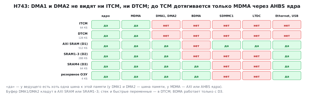
The main difference from the F7: on the H743 DMA1 and DMA2 do not see DTCM. And DTCM is
where data goes by default: in the template linker scripts
from the pack (GCC for H745/H747, the Keil example for H743I-EVAL) variables, heap
and stack sit from address 0x2000 0000. A global buffer declared as
on the F407 ends up in DTCM, and DMA gets a bus error on it — the transfer error flag
instead of data. DMA1/DMA2 buffers
go to AXI SRAM or SRAM1–3, BDMA buffers only to SRAM4, and into TCM
data is carried only by MDMA.
11б.3 Cache and DMA: two directions
DMA works with memory bypassing the core's cache. Hence two troubles — one per direction. A PC model: a cache with 32-byte lines and write-back, a 64-byte buffer, DMA reads and writes RAM directly.
| Experiment | Wrong bytes at the receiver |
|---|---|
| transmit: the core filled the buffer, DMA took it without cleaning | 64 of 64 |
transmit with SCB_CleanDCache_by_Addr before the start |
0 |
| receive: the core had read the buffer before, DMA put new data, no invalidate | 64 of 64 |
receive with SCB_InvalidateDCache_by_Addr after reception |
0 |
On transmit the new data is in the cache, and DMA takes the old data from RAM. On receive the new data is in RAM, and the core reads from the cache the lines it read earlier. The CMSIS operations fix this: clean before transmitting (write dirty lines out to memory), invalidate after receiving (forget the lines so that the next read comes from memory):
#define BUF_LEN  64u                    /* кратно 32: буфер занимает строки целиком */

static uint8_t tx_buf[BUF_LEN] __attribute__((aligned(32)));
static uint8_t rx_buf[BUF_LEN] __attribute__((aligned(32)));

void tx_start(DMA_Stream_TypeDef *s, uint32_t n)
{
    SCB_CleanDCache_by_Addr(tx_buf, (int32_t)n);   /* вытолкнуть в ОЗУ то, что записало ядро */
    s->M0AR = (uint32_t)tx_buf;
    s->NDTR = n;
    s->CR |= DMA_SxCR_EN;
}

void rx_done(uint32_t n)
{
    SCB_InvalidateDCache_by_Addr(rx_buf, (int32_t)((n + 31u) & ~31u));   /* забыть старые строки */
}
volatile solves nothing here: it forbids the compiler to keep
a value in a register, but the read still goes through the cache (section 124).
11б.4 The trap: a buffer shares a line with a neighbour
Cache operations work on whole lines: SCB_InvalidateDCache_by_Addr
in CMSIS rounds the range out to the boundaries of the lines it touches. If a receive
buffer does not start on a 32-byte boundary, its first line is shared with something
else — for example, a counter the core changes while DMA is receiving.
Model: line 0x300…0x31F, the first 16 bytes hold a counter, a 64-byte buffer starts
at 0x310. During reception the core incremented the
counter 1000 times (the line is dirty, in memory it is still 0), then DMA finished.
| After reception | Counter | Wrong bytes in the buffer |
|---|---|---|
| invalidate the buffer range | 0 of 1000 | 0 |
| clean and invalidate the buffer range | 1000 | 16 |
| buffer aligned to 32 and a multiple of 32, invalidate | 1000 | 0 |
The invalidate threw the dirty counter out of the cache as well — a thousand increments were lost.
Cleaning before invalidating saved the counter, but wrote the whole line to memory —
together with the stale start of the buffer, over what DMA had just put there.
There is no correct order of operations here: a DMA buffer must occupy whole
lines — the start aligned to 32 bytes (aligned(32)), the length a multiple of 32.
Then it shares no line with its neighbours, and a plain invalidate
is safe.
11б.5 The second way: a non-cacheable MPU region
Instead of maintaining the cache, the buffers can be placed where there is no cache at all: in TCM (if DMA reaches it — on the F7 yes, on the H7 only MDMA) or in a region that the MPU (section 11а) marks as normal non-cacheable memory:
/* Второй путь: область 32 КБ, которую кэш не трогает вовсе (TEX = 1, C = 0, B = 0) */
void mpu_dma_region(uint32_t base)
{
    ARM_MPU_Disable();
    ARM_MPU_SetRegion(ARM_MPU_RBAR(0u, base),
                      ARM_MPU_RASR(1u, ARM_MPU_AP_FULL, 1u, 0u, 0u, 0u, 0x00u, ARM_MPU_REGION_SIZE_32KB));
    ARM_MPU_Enable(MPU_CTRL_PRIVDEFENA_Msk);
}
In the model such a region gives zero wrong bytes in both directions without a single
cache operation. The price is speed: the core accesses these buffers
with full RAM latency. DMA buffers are collected into one section of the linker
script (.dma_buffers at the start of SRAM1 on the H743), so that the MPU region
covers all of them and nothing else; the region base is a multiple of its size.
| Way | What to do | Price |
|---|---|---|
| cache maintenance | clean before transmit, invalidate after receive; 32 alignment | easy to forget one operation |
| non-cacheable region | one MPU setup at startup | slow core access to the buffers |
| TCM | nothing | on the H7 not reachable by DMA1/DMA2; on the F7 only DTCM |
11б.6 What to put in TCM
TCM is the fastest memory of the core, and there is little of it. A sensible split:
- ITCM — code where latency matters: interrupt handlers,
the inner loop of a filter, functions that run while Flash is being erased.
Such functions are marked with the
.itcm_textsection (orRAMFUNCin ST examples) and copied from Flash to ITCM at startup — like.datain section 11. - DTCM — the stack, the heap, hot variables. On the F7 also DMA buffers, on the H7 not.
- Peripheral buffers — in the ordinary RAM of the domain where their DMA sits: DMA1/DMA2 — AXI SRAM or SRAM1–3, BDMA — SRAM4, Ethernet and USB — SRAM1–3.
11б.7 Pitfalls
- A DMA buffer in DTCM on the H7. DMA1 and DMA2 cannot reach it; the transfer ends with the error flag. On the F7 the same code works — the port breaks silently.
- Cleaning without alignment. The buffer shares a line with a neighbouring variable: invalidating loses the neighbour's changes, cleaning spoils the start of the received data. Align to 32 bytes and make the length a multiple of 32.
- Invalidating before reception instead of after. The core may manage to read the buffer and bring the lines back into the cache while DMA is working — and not only at your command: the core reads cacheable memory speculatively on its own. Invalidate after reception has finished (or both before and after).
volatileinstead of cache maintenance. The compiler stops caching the value in a register, but the hardware cache remains.- The cache was switched on, but the buffers were left as on the F407. All the DMA code that worked on the F4 has to be gone through again: every buffer gets alignment, cleaning or invalidation, or a non-cacheable region.
- An MPU region of the wrong size. The base of an MPU region is a multiple of its size; a 32 KB region with a base not on a 32 KB boundary will not cover what was expected.
- BDMA and SRAM1. BDMA works only in domain D3: SRAM4 and backup RAM.
11б.8 Summary
- The M7 has instruction and data caches of 4 KB each on the F746 and 16 KB each on the H743, the line is 32 bytes; RAM by default is write-back with write allocate.
- F746: ITCM 16 KB — core only, DTCM 64 KB — core and DMA through AHBS, SRAM1 240 KB and SRAM2 16 KB — everyone.
- H743: ITCM 64 KB and DTCM 128 KB — core and MDMA; DMA1/DMA2 — AXI SRAM and SRAM1–3; BDMA — only SRAM4 and backup RAM.
- Transmit without cleaning and receive without invalidating — 64 wrong bytes of 64 in the model; with the CMSIS operations — zero.
- An unaligned buffer breaks its neighbour: invalidating loses 1000 counter increments of 1000, clean plus invalidate spoils 16 bytes of the received data. Alignment to 32 and a length that is a multiple of 32 remove the problem.
- A non-cacheable MPU region does without cache maintenance, but is slower for the core.
Full sources
cache11b.c — DMA buffers on Cortex-M7: alignment, cache maintenance, non-cacheable MPU region.
/* 11б: буферы DMA на Cortex-M7 — выравнивание, обслуживание кэша, некэшируемая область MPU.
   Собирается armclang для STM32F746 и STM32H743 (проверка _verify/cache11b_check.py). */
#include <stdint.h>

#define BUF_LEN  64u                    /* кратно 32: буфер занимает строки целиком */

static uint8_t tx_buf[BUF_LEN] __attribute__((aligned(32)));
static uint8_t rx_buf[BUF_LEN] __attribute__((aligned(32)));

void cache_on(void)
{
    SCB_EnableICache();
    SCB_EnableDCache();                 /* после сброса оба кэша выключены */
}

void tx_start(DMA_Stream_TypeDef *s, uint32_t n)
{
    SCB_CleanDCache_by_Addr(tx_buf, (int32_t)n);   /* вытолкнуть в ОЗУ то, что записало ядро */
    s->M0AR = (uint32_t)tx_buf;
    s->NDTR = n;
    s->CR |= DMA_SxCR_EN;
}

void rx_done(uint32_t n)
{
    SCB_InvalidateDCache_by_Addr(rx_buf, (int32_t)((n + 31u) & ~31u));   /* забыть старые строки */
}

uint8_t rx_byte(uint32_t i) { return rx_buf[i]; }
uint8_t *tx_area(void) { return tx_buf; }

/* Второй путь: область 32 КБ, которую кэш не трогает вовсе (TEX = 1, C = 0, B = 0) */
void mpu_dma_region(uint32_t base)
{
    ARM_MPU_Disable();
    ARM_MPU_SetRegion(ARM_MPU_RBAR(0u, base),
                      ARM_MPU_RASR(1u, ARM_MPU_AP_FULL, 1u, 0u, 0u, 0u, 0x00u, ARM_MPU_REGION_SIZE_32KB));
    ARM_MPU_Enable(MPU_CTRL_PRIVDEFENA_Msk);
}
Next: section 11в "Read protection on the F1: why level 1 does not save the firmware" — what RDP level 1 promises and why it is not a safe.