 Embedded HandbookApps
10. Power and power saving
A device powered from a wall socket may never sleep. A device powered from a battery must sleep almost always: the difference between a running and a sleeping chip is four orders of magnitude, and it is exactly what decides whether the product lives a week or three years.
10.1 Three sleep modes
Terms used in the documentation
Term Meaning low-power modes modes with reduced consumption Sleep / Stop / Standby the three sleep depths, from light to deep wakeup pin a pin that wakes the chip backup domain the part that runs from VBAT voltage regulator the internal regulator that powers the core low-power regulator the economical mode of the regulator programmable voltage detector (PVD) a supply level detector with a programmable threshold power reset / brown-out reset a reset on power-up / on a supply dip to retain the content to keep the contents wakeup latency the time to leave the mode send event on pending (SEVONPEND) an event on a pending interrupt burden voltage the voltage drop across the ammeter average current the current averaged over time debug in low-power modes debugging while the chip sleeps
| Sleep | Stop | Standby | |
|---|---|---|---|
| core | stopped | stopped | off |
| peripherals | running | stopped | off |
| RAM contents | retained | retained | lost |
| peripheral registers | retained | retained | lost |
| exit | any interrupt | EXTI, RTC, IWDG | the WKUP pin, RTC, reset |
| after exit | continues from the same line | continues, but the clocks are reset to HSI | reset, the program starts over |
| exit time | cycles | microseconds | tens to hundreds of µs |
| consumption (F103, order) | units to tens of mA | tens of µA | units of µA |
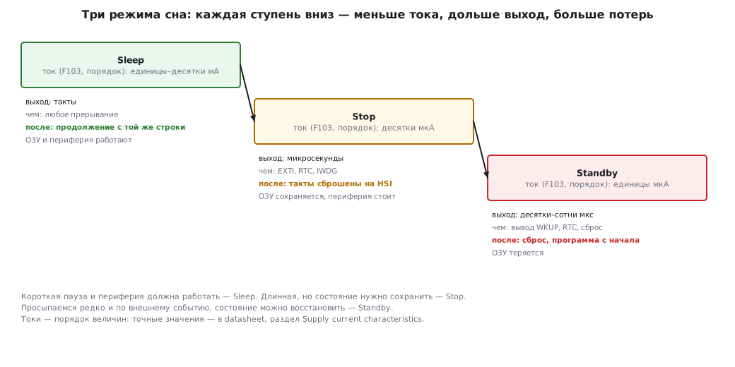
The exit time is counted up to the first program instruction: from Standby on F103 it is 50 µs, on F407 — 375 µs. But after Standby the program starts over: starting the crystal (about 2 ms), the PLL and the start-up code add milliseconds.
The figures are given as orders of magnitude: the exact values depend on temperature, voltage and what is enabled. They should be looked up in the datasheet, section Supply current characteristics — there are tables for each mode there.
How to choose. If the pause is short (milliseconds between sensor polls) and the peripherals must keep working — Sleep. If the pause is long but the program state must be kept — Stop. If the device wakes up rarely and on an external event, and the state can be restored — Standby.
10.2 Sleep: only the core stops
The simplest mode. The core stops, everything else keeps working: timers count, the UART receives, DMA transfers.
void enter_sleep(void)
{
    SCB->SCR &= ~SCB_SCR_SLEEPDEEP_Msk;   /* обычный сон, не глубокий */
    __WFI();                              /* Wait For Interrupt */
    /* Проснулись ровно здесь: контекст цел. */
}
If SysTick is running in the program (with HAL it always is), it wakes the core every
millisecond. For the duration of sleep it is stopped — HAL_SuspendTick() or
SysTick->CTRL &= ~SysTick_CTRL_TICKINT_Msk — and after wake-up it is switched
back on.
__WFI() is the core instruction "wait for interrupt". There is also __WFE() — "wait
for event"; it also reacts to events without calling a handler (the very
GPIO_MODE_EVT_* modes from section 8).
A useful technique is the SLEEPONEXIT bit: with it the core automatically falls asleep on
exit from every handler. The program becomes a set of reactions
to interrupts, and between them the chip sleeps:
SCB->SCR |= SCB_SCR_SLEEPONEXIT_Msk;
Another bit of this register, SEVONPEND, makes any interrupt that becomes pending
an event for __WFE() — even one disabled in the NVIC. The chip wakes up,
but the handler is not called: this is how a peripheral flag is waited for without an interrupt handler.
10.3 Stop: the clocks are stopped, memory is intact
All oscillators stop, but the contents of RAM and registers are retained. The chip wakes up on an external interrupt, an RTC alarm or the watchdog timer.
There is also an entry condition: all pending EXTI flags, peripheral interrupt flags
and the RTC alarm flag must be cleared. If even one
is pending, Stop will not happen — the program will simply continue after WFI.
The EXTI flags are all cleared at once with the line EXTI->PR = EXTI->PR;: a flag
is cleared by writing a one, and this way everything pending goes away.
void enter_stop(void)
{
    RCC->APB1ENR |= RCC_APB1ENR_PWREN;    /* доступ к регистрам питания */

    PWR->CR &= ~PWR_CR_PDDS;              /* 0 -> Stop, а не Standby */
    PWR->CR |= PWR_CR_LPDS;               /* регулятор в экономичный режим */
    SCB->SCR |= SCB_SCR_SLEEPDEEP_Msk;    /* глубокий сон */

    __WFI();

    /* ← сюда возвращаемся после пробуждения */
    SCB->SCR &= ~SCB_SCR_SLEEPDEEP_Msk;
    SystemClock_72MHz();                  /* обязательно! см. ниже */
}
⚠️ The main pitfall of the whole section. After leaving Stop the system is clocked from HSI, not from your PLL. The crystal is off, the multiplier is reset. The program continues from the same line and looks working, but runs nine times slower: delays stretch, the UART spits garbage, PWM changes frequency. The clock configuration from section 6 must be applied again — first thing after wake-up.
Note that Stop and Standby differ by one bit, PDDS.
They are easy to confuse, and the consequences differ: in the second case the program
will not continue but will start over.
10.4 Standby: exit through reset
Almost everything is switched off, including the main regulator. Only the backup domain stays alive. Consumption is a few microamperes, that is, the chip can wait for years.
void enter_standby(void)
{
    RCC->APB1ENR |= RCC_APB1ENR_PWREN;

    PWR->CSR |= PWR_CSR_EWUP;             /* разрешить вывод WKUP (PA0) */
    PWR->CR |= PWR_CR_PDDS;               /* 1 -> Standby */
    PWR->CR |= PWR_CR_CWUF;               /* сбросить флаг — после EWUP */
    SCB->SCR |= SCB_SCR_SLEEPDEEP_Msk;

    __WFI();
    /* Сюда исполнение уже не вернётся. */
}
Wake-up from Standby is a reset: the program starts from Reset_Handler,
RAM is lost (there are random values there; the zeros in .bss are written again by the start-up
code), the peripherals are in their initial state. Such a start can be told from an ordinary
power-up by a flag:
uint8_t woke_from_standby(void)
{
    RCC->APB1ENR |= RCC_APB1ENR_PWREN;
    if (PWR->CSR & PWR_CSR_SBF) {
        PWR->CR |= PWR_CR_CSBF;           /* сбросить признак */
        return 1u;
    }
    return 0u;
}
⚠️ Clear
CWUFbefore entry, last of all. If the wake-up flag stays set, the chip will leave Standby instantly — and you will see an endless reboot instead of sleep. On F1 enablingEWUPwith a high level onPA0sets the flag by itself, soCWUFis set afterEWUP, right before__WFI.
10.5 The backup domain
A separate area powered from the VBAT pin — usually from a lithium cell
or a supercapacitor. It keeps working when everything else is unpowered.
What lives there:
- the real-time clock — counts the date and time with the main power removed;
- backup registers — on F1 10 or 42
BKPregisters of 16 bits (20 bytes on medium-density, 84 on high-density), on F4 20RTC_BKPxRregisters of 32 bits (80 bytes). They survive both Standby and a complete power-off. F405/F407 also have 4 KB of backup RAMBKPSRAM(clock —RCC_AHB1ENR_BKPSRAMEN; for it to be held fromVBAT, its regulator is enabled with theBREbit inPWR->CSR); - the tamper detector — records an external intrusion.
Writing there is protected, and the protection must be removed explicitly:
void backup_domain_write(uint32_t value)
{
    RCC->APB1ENR |= RCC_APB1ENR_PWREN | RCC_APB1ENR_BKPEN;
    PWR->CR |= PWR_CR_DBP;                /* снять защиту записи */
    BKP->DR1 = (uint16_t)value;
    PWR->CR &= ~PWR_CR_DBP;               /* вернуть защиту */
}
A forgotten DBP is the typical cause of "I write to a backup register, but it does not change".
There is no error, the write is simply ignored.
Backup registers are convenient precisely for Standby: save before sleep what must not be lost, and read it after wake-up.
10.6 What can wake it up
| Source | From Sleep | From Stop | From Standby |
|---|---|---|---|
| any peripheral interrupt | yes | no | no |
| an external EXTI interrupt | yes | yes | no |
| RTC alarm | yes | yes | yes |
| the IWDG watchdog | through reset | through reset | through reset |
the WKUP pin (PA0) |
yes | yes | yes |
the NRST signal |
yes | yes | yes |
The key point: from Standby only WKUP, RTC and reset wake the chip. Ordinary pins do not
work there — the EXTI controller is unpowered. If the device must wake up
on a button press, the button is wired to PA0.
For periodic wake-up the RTC is used: it is clocked from LSE or LSI, which keep running in the backup domain.
A running watchdog does not stop in sleep. On F1 and F4 IWDG cannot
be switched off either by the program or by sleep: it counts in both Stop and Standby. If the sleep
is longer than its period (on F1 no more than 4096 × 256 / 40 kHz ≈ 26 s), the chip
will reboot. Then the RTC wakes the chip ahead of time, the program refreshes
the watchdog and falls asleep again. On L4, G0 and G4 the watchdog is frozen in Stop and Standby
by the option bits IWDG_STOP and IWDG_STDBY.
10.7 The voltage detector (PVD)
It compares the supply with a threshold and reports when it has dropped. This is not a reset but a warning: the program has time left to save data to Flash or backup registers while the capacitors still hold their charge.
PWR->CR = (PWR->CR & ~PWR_CR_PLS) | PWR_CR_PLS_2V7;   /* порог 2,7 В */
PWR->CR |= PWR_CR_PVDE;         /* включить детектор */
EXTI->RTSR |= EXTI_RTSR_TR16;   /* нарастающий фронт PVDO: питание упало ниже порога */
EXTI->IMR  |= EXTI_IMR_MR16;
NVIC_EnableIRQ(PVD_IRQn);
Useful in products where the power may go off at any moment: meters, loggers, anything where an interruption in the middle of a write corrupts data.
10.8 How to measure the sleep current
The figures in table 10.1 are an order of magnitude, not a promise. Your own device has to be measured: a forgotten pull resistor or the debugger easily add more than the sleeping chip itself draws. And measuring is harder than it seems: within milliseconds the current changes by hundreds of times.
The example for the whole subsection is a sensor powered from two AA cells (3.0 V, about 2500 mAh). Once a second it wakes up for 5 ms and draws 10 mA during that time, the rest of the time it sleeps in Stop at 20 µA.
Where to connect the instrument. The ammeter is put into the supply line of the chip itself,
not of the whole board: the regulator and the board's power LED also draw current, often
more than the sleeping chip. Nucleo boards have the IDD jumper for this: if it is
removed, only the microcontroller's supply is broken.
The instrument itself interferes. An ammeter is a shunt, and voltage drops across it. In a simple 3½-digit multimeter the shunt of each range is chosen so that full scale gives 200 mV across it:
| Range | Shunt | Sleep, 20 µA | Wake-up, 10 mA |
|---|---|---|---|
| 200 µA | 1 kΩ | 20 mV, step 0.1 µA | 10 V needed — impossible |
| 2 mA | 100 Ω | 2 mV, step 1 µA | 1 V: 2.0 V remains |
| 20 mA | 10 Ω | 0.2 mV, step 10 µA | 0.1 V |
On the 200 µA range no more than (3.0 − 2.0) V / 1 kΩ = 1.0 mA will pass through the instrument. When trying to wake up, the supply sags below 2.0 V — the lower limit for F103. For a while the chip runs on the charge of the capacitors (10 µF at a current of 10 mA discharge by a volt in a millisecond), and then goes into reset. A short wake-up sometimes gets through, a long one never does, and from the outside this looks like a mysterious failure. On the 2 mA range the chip wakes up exactly at the limit of what is allowed, and on the 20 mA range the sleep current can no longer be seen.
Hence the technique: a jumper in parallel with the instrument. Start-up and wake-ups go through the closed jumper, and when the chip has fallen asleep, it is opened and the reading is taken.
The multimeter averages the wrong thing. The reading updates two or three times a second and is averaged over a window of about 100 ms. If a burst fell into the window, the instrument shows (10 mA · 5 ms + 20 µA · 95 ms) / 100 ms = 519 µA; if it did not — 20 µA. The reading jumps between these numbers, and the real average, about 70 µA, is shown by neither of them.
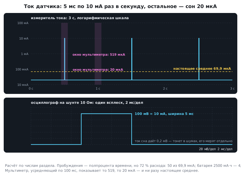
Three measurements instead of one.
- Sleep current. Wake-ups are switched off (or the alarm is set to a minute), the 200 µA range, the jumper.
- The burst. A 10 Ω shunt in the supply and an oscilloscope: 10 mA gives 100 mV across it, the height and width of the pulse can be seen. The sleep current on the same shunt gives 0.2 mV and drowns in noise, which is why it is measured separately.
- Average current. It is calculated:
I_ср = I_акт · t_акт / T + I_сна · (1 − t_акт / T)
     = 10 мА · 0,005 + 20 мкА · 0,995 = 50 + 19,9 = 69,9 мкА
Instruments that measure everything at once do exist — these are current meters with automatic range switching. The task is not easy for them: the current changes 500-fold, and to see the sleep current with 1 % accuracy you need 10 mA / 0.2 µA = 50 000 counts. That is 25 times more than a 3½-digit multimeter has.
What the calculation gives. Five milliseconds out of a thousand — half a percent of the time — give 50 of the 69.9 µA, that is 72 % of the consumption. A 2500 mAh battery will last 2500 / 0.0699 ≈ 35 800 h, which is 4.1 years. What happens if you change one part at a time:
| What was changed | Average current | Battery life |
|---|---|---|
| nothing | 69.9 µA | 4.1 years |
| a burst half as long, 2.5 ms | 45 µA | 6.3 years |
| half the sleep current, 10 µA | 60 µA | 4.8 years |
| a forgotten pull-up on a pin held to ground | 145 µA | 2.0 years |
A burst half as long added more than two years, and half the sleep current eight months. Hunting for sleep microamperes is worth it when the active part has already been squeezed. The built-in pull resistor is about 40 kΩ. If a pin is held to ground externally by a pressed button or by the output of a neighbouring chip, through it flows 3.0 V / 40 kΩ = 75 µA — more than the whole average current of the example. One such pull resistor halves the battery life.
Preparing the chip for the measurement. Unused pins are put into analog
mode: it has the input trigger switched off, and a floating input draws no current. On F1 this is
four zero bits in CRL/CRH, on F4 two ones in MODER. After reset
the pins of both F1 and F4 are inputs (except the debug pins), so you have to switch them
yourself; on G4 and L4 the pins are already analog after reset.
/* keep — выводы порта, которые трогать нельзя (1 — оставить как есть) */
void port_to_analog(GPIO_TypeDef *port, uint16_t keep)
{
#if defined(STM32F10X_MD)
    uint32_t lo = 0, hi = 0;                /* по четыре бита на вывод */
    for (int i = 0; i < 8; i++) {
        if (keep & (1u << i))       lo |= 0xFu << (4 * i);
        if (keep & (1u << (i + 8))) hi |= 0xFu << (4 * i);
    }
    port->CRL &= lo;                        /* аналоговый вход у F1 — 0000 */
    port->CRH &= hi;
#elif defined(STM32F407xx)
    uint32_t m = 0;                         /* по два бита на вывод */
    for (int i = 0; i < 16; i++)
        if (keep & (1u << i))
            m |= 3u << (2 * i);
    port->MODER |= ~m;                      /* аналоговый режим у F4 — 11 */
    port->PUPDR &= m;                       /* и подтяжки снять */
#endif
}

void sleep_measure_prepare(void)
{
#if defined(STM32F10X_MD)                   /* без такта запись в порт не проходит */
    RCC->APB2ENR |= RCC_APB2ENR_IOPAEN | RCC_APB2ENR_IOPBEN | RCC_APB2ENR_IOPCEN;
#elif defined(STM32F407xx)
    RCC->AHB1ENR |= RCC_AHB1ENR_GPIOAEN | RCC_AHB1ENR_GPIOBEN | RCC_AHB1ENR_GPIOCEN;
#endif
    port_to_analog(GPIOA, (1u << 13) | (1u << 14));   /* SWDIO и SWCLK */
    port_to_analog(GPIOB, 0);
    port_to_analog(GPIOC, (1u << 14) | (1u << 15));   /* кварц часов LSE */
    debug_off_in_sleep();
}
The debug pins PA13 and PA14 are left as they are: in analog mode the programmer may lose the connection with the chip, and flashing will require connecting under reset. The clock crystal pins PC14 and PC15 are left in case the RTC wakes the chip from LSE. The other ports are handled in the same way.
The debugger. To avoid losing the chip in sleep, the debugging environment sets in DBGMCU->CR
the bits DBG_SLEEP, DBG_STOP and DBG_STANDBY — and in Stop the clocks
from HSI keep running: instead of tens of microamperes you get a current of the Sleep order. The reset button
does not clear these bits, only a power-off clears them. So after
debugging the power is cycled or the bits are cleared by yourself (on F1 only the
first way is reliable: without a debugger DBGMCU_CR is not accessible to the program, section 2а.4):
void debug_off_in_sleep(void)
{
    DBGMCU->CR &= ~(DBGMCU_CR_DBG_SLEEP | DBGMCU_CR_DBG_STOP | DBGMCU_CR_DBG_STANDBY);
}
10.9 F0 and G0: F0 is like F1, G0 has a mode field
F0 repeats F1 down to the bit: two registers PWR->CR and PWR->CSR, Stop
and Standby differ by PDDS, the regulator by LPDS, the flags are cleared by
CWUF/CSBF, the wake-up pin is enabled by EWUP1. There is one difference: after Stop
the system starts from the 8 MHz HSI, and the 48 MHz from 6.7 must be enabled again.
    PWR->CR &= ~PWR_CR_PDDS;                    /* 0 -> Stop, а не Standby */
    PWR->CR |= PWR_CR_LPDS;                     /* регулятор в экономичный режим */
    SCB->SCR |= SCB_SCR_SLEEPDEEP_Msk;
    __WFI();
G0 is built differently, and this design is shared with L4, G4, U5: the sleep mode is
not a set of bits but the three-bit field LPMS in CR1. The values come from the
LL header stm32g0xx_ll_pwr.h:
LPMS |
Mode | What remains |
|---|---|---|
| 000 | Stop 0 | RAM, the regulators in normal mode — fast exit |
| 001 | Stop 1 | RAM, the regulator in low-power mode |
| 011 | Standby | only the backup domain and, optionally, part of RAM |
| 100 | Shutdown | nothing but the backup domain: no RAM and no voltage detector |
The wake-up flags are read in SR1 and cleared by writing ones to a separate
register SCR; the wake-up pins are EWUP1 in CR3. F0/F1 code does not
build on G0: no member named 'CR' in 'PWR_TypeDef', PWR_CR_PDDS
is not declared.
    PWR->CR1 = (PWR->CR1 & ~PWR_CR1_LPMS) | LL_PWR_MODE_STOP1;   /* Stop 1: регулятор в экономичном режиме */
    SCB->SCR |= SCB_SCR_SLEEPDEEP_Msk;
    __WFI();
    PWR->SCR = PWR_SCR_CWUF1 | PWR_SCR_CSBF;    /* флаги — записью единиц в SCR, а не в CR */
    PWR->CR3 |= PWR_CR3_EWUP1;                  /* вывод WKUP1 (PA0) */
    PWR->CR1 = (PWR->CR1 & ~PWR_CR1_LPMS) | LL_PWR_MODE_STANDBY;
Two modes that F0 and F1 do not have at all. Shutdown is deeper than Standby:
even the voltage detector is off, RAM is not retained, exit is a reset.
Low-power run (LPR in CR1): the core keeps
executing code, but the regulator is in low-power mode — suitable
for slow tasks between sleeps. After Stop G0 starts from HSI16 —
the 64 MHz from 6.7 is enabled again, as on F0.
10.10 Pitfalls
A forgotten clock for PWR. The power registers are on APB1, and without
RCC_APB1ENR_PWREN writes to them do not go through. Silently.
The clocks are not restored after Stop. Covered above — the most frequent and the least noticeable error of the mode.
Stop does not happen, the current is as when running. A flag is pending: a pending one in
EXTI->PR — often from the button that woke the chip last time — a
peripheral interrupt flag or the RTC alarm flag. WFI then does not put it to sleep, and
the program continues. Clear the flags before entry (10.3).
CWUF was not cleared or was cleared before EWUP. An instant exit from Standby
that looks like a reboot after a failure.
The debugger interferes with measuring. While ST‑Link is connected, some blocks stay
powered: the DBG_* bits in DBGMCU->CR keep the clocks running in Stop, and the consumption
looks much higher than the real one. The reset button does not clear these bits — after
debugging you must cycle the power or clear them in software (10.8).
The ammeter drops the supply. On the 200 µA range the multimeter's shunt is 1 kΩ, and the chip cannot wake up: the supply sags, and the wake-up turns into a reset. A jumper in parallel with the instrument saves the day (10.8).
Pins in an undefined state. Current leaks not only through the core: an input left "floating" may draw more than the sleeping chip. Before sleep it makes sense to put unused pins into analog mode — its consumption is zero (section 8, a ready function is in 10.8).
Peripherals keep eating current. In Sleep everything that is enabled runs: timers,
the ADC, USB. If the goal is to save power, whatever is unnecessary must be switched off in RCC before falling asleep.
Waking up too often. Leaving Stop takes microseconds, and leaving Standby together with restarting the program takes milliseconds, and each time it is a current burst. Waking up a hundred times a second for the sake of Standby is pointless — the gain is eaten by the transitions.
10.11 Summary
- Three modes: Sleep (the core sleeps), Stop (the clocks sleep, memory is intact), Standby (everything is off except the backup domain).
- Stop and Standby are distinguished by one bit,
PDDS, but the consequences differ: the program continues versus a reset. - After Stop the clocks are reset to HSI — the configuration from section 6 must be applied again.
- Stop happens only if the pending flags of EXTI, the peripherals
and the RTC alarm are cleared; otherwise the program continues after
WFI. - Leaving Standby is a reset; it can be told from a cold start
by the
SBFflag. - Before entering Standby
CWUFmust be cleared — last, afterEWUP, — otherwise the chip will wake up immediately. - From Standby only
WKUP, RTC and reset wake the chip — ordinary pins are dead there. - The backup domain survives everything: the RTC and a few dozen bytes of memory are there.
Writing is opened by the
DBPbit. - Sleep current, the burst and the average current are three different measurements: an ammeter on a microampere range drops the supply at wake-up, and the multimeter's averaging matches neither the sleep nor the average. The average current is calculated by the formula.
- With wake-up once a second, battery life is decided above all by the length of the burst; one forgotten pull resistor on a pin held low halves it.
- Before the measurement unused pins are put into analog mode (except SWD)
and the debug bits in
DBGMCU->CRare cleared — the reset button does not clear them.
Full sources
pwr_f0.c — STM32F072 sleep modes: PWR registers as on F1.
/* Раздел 10.9: режимы сна STM32F072 — регистры PWR как у F1: CR и CSR. */
#include <stddef.h>
#include "stm32f0xx.h"

_Static_assert(offsetof(PWR_TypeDef, CSR) == 0x04u, "у F0 два регистра PWR — CR и CSR, как у F1");

void enter_stop_f0(void)
{
    RCC->APB1ENR |= RCC_APB1ENR_PWREN;
    PWR->CR &= ~PWR_CR_PDDS;                    /* 0 -> Stop, а не Standby */
    PWR->CR |= PWR_CR_LPDS;                     /* регулятор в экономичный режим */
    SCB->SCR |= SCB_SCR_SLEEPDEEP_Msk;
    __WFI();
    SCB->SCR &= ~SCB_SCR_SLEEPDEEP_Msk;
    /* после Stop система тактируется от HSI 8 МГц — 48 МГц из 6.7 включить заново */
}

void enter_standby_f0(void)
{
    RCC->APB1ENR |= RCC_APB1ENR_PWREN;
    PWR->CR |= PWR_CR_CWUF;                     /* сбросить флаг пробуждения */
    PWR->CR |= PWR_CR_PDDS;                     /* 1 -> Standby */
    PWR->CSR |= PWR_CSR_EWUP1;                  /* вывод WKUP1 (PA0) */
    SCB->SCR |= SCB_SCR_SLEEPDEEP_Msk;
    __WFI();
}
pwr_g0.c — STM32G071 sleep modes: the LPMS field, clearing flags through SCR, wake-up pins in CR3.
/* Раздел 10.9: режимы сна STM32G071 — режим выбирает поле LPMS в CR1,
 * флаги сбрасываются записью в SCR, будящие выводы разрешают в CR3. */
#include <stddef.h>
#include "stm32g0xx.h"
#include "stm32g0xx_ll_pwr.h"

_Static_assert(offsetof(PWR_TypeDef, SCR) == 0x18u && offsetof(PWR_TypeDef, SR1) == 0x10u, "SR1 и SCR");
_Static_assert(LL_PWR_MODE_STOP0 == 0u && LL_PWR_MODE_STOP1 == PWR_CR1_LPMS_0
               && LL_PWR_MODE_STANDBY == (PWR_CR1_LPMS_1 | PWR_CR1_LPMS_0) && LL_PWR_MODE_SHUTDOWN == PWR_CR1_LPMS_2,
               "LPMS: 000 Stop 0, 001 Stop 1, 011 Standby, 100 Shutdown");

void enter_stop1_g0(void)
{
    RCC->APBENR1 |= RCC_APBENR1_PWREN;
    PWR->CR1 = (PWR->CR1 & ~PWR_CR1_LPMS) | LL_PWR_MODE_STOP1;   /* Stop 1: регулятор в экономичном режиме */
    SCB->SCR |= SCB_SCR_SLEEPDEEP_Msk;
    __WFI();
    SCB->SCR &= ~SCB_SCR_SLEEPDEEP_Msk;
    /* после Stop система тактируется от HSI16 — 64 МГц из 6.7 включить заново */
}

void enter_standby_g0(void)
{
    RCC->APBENR1 |= RCC_APBENR1_PWREN;
    PWR->SCR = PWR_SCR_CWUF1 | PWR_SCR_CSBF;    /* флаги — записью единиц в SCR, а не в CR */
    PWR->CR3 |= PWR_CR3_EWUP1;                  /* вывод WKUP1 (PA0) */
    PWR->CR1 = (PWR->CR1 & ~PWR_CR1_LPMS) | LL_PWR_MODE_STANDBY;
    SCB->SCR |= SCB_SCR_SLEEPDEEP_Msk;
    __WFI();
}

/* Чего нет у F0 и F1: работа на пониженном напряжении регулятора (LPR)
 * и Shutdown — глубже Standby, без ОЗУ и без часов сна. */
void enter_shutdown_g0(void)
{
    PWR->CR1 = (PWR->CR1 & ~PWR_CR1_LPMS) | LL_PWR_MODE_SHUTDOWN;
    SCB->SCR |= SCB_SCR_SLEEPDEEP_Msk;
    __WFI();
}
Next: section 10а "Low power on L4 and U5" — Stop 2, Stop 3, Shutdown and why a battery lives only a quarter longer with them.