 Embedded HandbookApps
9а. GPDMA on STM32U5: linked lists, triggers and ring reception without interrupts
Section 9 took apart DMA on F1 and F4: channels and streams, the CIRC bit, the
NDTR counter. STM32U5 does not have that controller. In its place is GPDMA: it has
no CIRC bit, no double buffering and no mapping table. All of this
is replaced by one mechanism — the linked list: a chain of transfer descriptions
in memory that the channel walks through by itself. Here — how the list is laid out in memory,
how to build from it a ring for UART reception (a comparison with 16б), two buffers
for the ADC and output of a table on a timer trigger; how LPDMA differs and what
TrustZone adds.
Prerequisites: the reference manual RM0456 (rev. 4), chapters 17 "GPDMA" and 18
"LPDMA", the header stm32u585xx.h and HAL 1.3.0 from the Keil pack STM32U5xx_DFP
2.2.1, the board package B-U585I-IOT02A_BSP 1.1.0. Our own code was built with armclang and
arm-none-eabi-gcc for Cortex-M33. The same code was run on a computer over
a model of the channel written from the text of RM0456, and the assembly of list items was
checked word for word against the HAL code. QEMU does not model U5, and nothing was run
on a board.
Terms used in the documentation
Term Meaning general purpose DMA (GPDMA) the general-purpose DMA controller low-power DMA (LPDMA) the DMA of the low-power domain linked-list item (LLI) one element of the linked list in memory linked-list register file the channel registers that the list updates link transfer loading the next item from memory update bits ( UT1,UT2,UB1,USA,UDA,ULL)which registers are in the item run-to-completion mode the list runs to the end by itself link step mode ( LSM)one item per enabling of the channel block / burst / beat a block / a burst / a single transfer request ( REQSEL) / trigger (TRIGSEL)a peripheral request / a trigger transfer complete event mode ( TCEM)at which level to raise "transfer complete" padding/alignment mode ( PAM)padding and alignment for different widths user setting error ( USEF)a configuration error update link error ( ULEF)a bus error while reading an item trigger overrun ( TOF)a lost trigger 2D addressing two-dimensional addressing
9а.1 What changed compared with F1 and F4
| F4 (section 9) | STM32U585 | |
|---|---|---|
| controllers | DMA1, DMA2 with 8 streams each | GPDMA1 — 16 channels, LPDMA1 — 4 channels |
| source selection | stream + the CHSEL field, mapping table |
any request on any channel: REQSEL |
| what defines a transfer | peripheral, memory, direction | source and destination, each with its own width and increment |
| counter | NDTR, in elements |
BNDT, in bytes |
| in a circle | the CIRC bit |
a linked list |
| two buffers | the DBM bit |
a linked list of two items |
| start on an event | none | trigger: TRIGSEL, TRIGPOL, TRIGM |
| flags | LISR/HISR for four streams |
each channel has its own CxSR, cleared in CxFCR |
| switching off | clear EN and wait |
SUSP, wait for SUSPF, RESET |
| protection | none | channels are divided into secure and privileged |
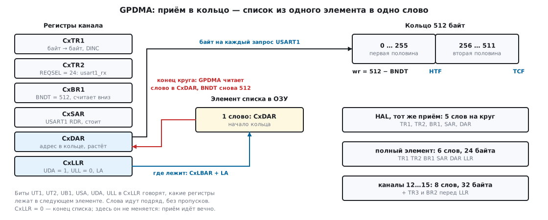
Requests. There is no mapping table. The request number is written into the REQSEL field
of the CxTR2 register — seven bits; in table 136 of the manual the numbers go from 0 to 125:
adc1_dma — 0, usart1_rx_dma — 24, usart1_tx_dma — 25. Conflicts of
"two blocks on one channel" are gone, but the opposite one appeared: one request
must not be given to two enabled channels, and the controller does not raise a configuration
error for it.
The channels are not equal (2д.4): channels 0…11 have an 8-byte queue and linear addressing, channels 12…15 — 32 bytes and two-dimensional. The queue is always there: a transfer goes in two steps — from the source into the queue and from the queue to the destination. GPDMA has no "without FIFO" mode as on F4.
Priority is the PRIO field in CxCR, four values. Value 3 is a separate
class: it is served before all others. Values 0, 1, 2 share the remaining
bus time with weights: according to the example in RM0456, a request with priority 0 next
to a request with priority 1 gets 1/4 of the remaining bandwidth against 3/4,
next to priority 2 — 1/6 against 5/6.
Names. In RM0456 the registers are called GPDMA_CxCR, GPDMA_CxTR1; in the header
these are the fields CCR, CTR1, CTR2, CBR1, CSAR, CDAR, CTR3, CBR2,
CLLR, CLBAR, CSR, CFCR of the DMA_Channel_TypeDef structure, and the bits are
DMA_CCR_EN, DMA_CTR2_REQSEL without a channel number. Channel x lies at offset
0x50 + 0x80 · x from the start of the controller. LPDMA1 has the same structure.
9а.2 The linked list: CxLBAR, CxLLR and the item in memory
Six channel registers describe one block transfer: CxTR1, CxTR2,
CxBR1, CxSAR, CxDAR and CxLLR. Channels 12…15 add
CxTR3 and CxBR2. When a block is finished, the channel looks at CxLLR:
CxLLR= 0 — the list has ended:TCFis raised, theENbit clears itself;- otherwise the channel reads the next item from memory and continues.
The item address is the upper 16 bits from CxLBAR (the LBA field) plus the lower 16
from CxLLR (the LA field, bits 15:2). Hence two rules of RM0456: an item
is aligned to 4 bytes, and the whole list of one channel lies within one
64 KB window. The remaining bits of CxLLR are update bits: which registers are
in the next item.
CxLLR bit |
Number | What to update from memory |
|---|---|---|
UT1 |
31 | CxTR1 |
UT2 |
30 | CxTR2 |
UB1 |
29 | CxBR1 |
USA |
28 | CxSAR |
UDA |
27 | CxDAR |
UT3 |
26 | CxTR3 — channels 12…15 only |
UB2 |
25 | CxBR2 — channels 12…15 only |
ULL |
16 | CxLLR itself |
An item is not a structure with fixed fields. It is words in a row, without
gaps: one for each bit that is set, in the order of the table. All
six bits — an item of 6 words (24 bytes); on channels 12…15 with all eight —
8 words (32 bytes). One bit — one word. It matters whose CxLLR it is: the layout
of an item is described by the bits of the previous item (for the first one — of the
register itself). The LLR word inside an item already describes the next one.
The types and constants on which all the listings of the section rely (gpdma.h):
/* Значения регистров одного элемента списка — в том порядке, в каком GPDMA читает их из памяти */
typedef struct {
    uint32_t tr1, tr2, br1, sar, dar;   /* есть у всех каналов */
    uint32_t tr3, br2;                  /* только каналы 12…15: двумерная адресация */
} lli_regs_t;

/* Биты обновления CxLLR: какие регистры лежат в следующем элементе */
#define LLI_UPD_LINEAR (DMA_CLLR_UT1 | DMA_CLLR_UT2 | DMA_CLLR_UB1 | DMA_CLLR_USA | DMA_CLLR_UDA | DMA_CLLR_ULL)
#define LLI_UPD_2D     (LLI_UPD_LINEAR | DMA_CLLR_UT3 | DMA_CLLR_UB2)

#define GPDMA_FLAGS    (DMA_CFCR_TCF | DMA_CFCR_HTF | DMA_CFCR_DTEF | DMA_CFCR_ULEF | DMA_CFCR_USEF \
                        | DMA_CFCR_SUSPF | DMA_CFCR_TOF)
#define GPDMA_ERRORS   (DMA_CSR_DTEF | DMA_CSR_ULEF | DMA_CSR_USEF)

#define GPDMA_W8   0u                   /* SDW_LOG2 / DDW_LOG2: двоичный логарифм ширины в байтах */
#define GPDMA_W16  1u
#define GPDMA_W32  2u
#define GPDMA_TRIG_RISING 1u            /* TRIGPOL */
#define GPDMA_TRIG_BLOCK  0u            /* TRIGM: триггер разрешает блок */
#define GPDMA_TRIG_LINK   2u            /*        загрузку следующего элемента */
#define GPDMA_TRIG_EACH   3u            /*        каждую пересылку */
Assembling an item and the CxLLR values (gpdma.c):
/* Сколько 32-битных слов занимает элемент, который описывают биты обновления upd */
uint32_t lli_words(uint32_t upd)
{
    uint32_t n = 0;
    for (upd &= LLI_UPD_2D; upd != 0u; upd &= upd - 1u)
        n++;
    return n;
}

/* Собрать элемент в памяти. upd — биты Uxx из CxLLR ПРЕДЫДУЩЕГО элемента (для первого — из самого
   регистра CxLLR): они говорят, какие регистры лежат в этом элементе. Слова идут подряд, без
   пропусков, в порядке TR1, TR2, BR1, SAR, DAR, TR3, BR2, LLR. llr — то, что попадёт в CxLLR:
   описание следующего элемента. Возвращает число записанных слов. */
uint32_t lli_pack(uint32_t *mem, const lli_regs_t *r, uint32_t upd, uint32_t llr)
{
    uint32_t n = 0;
    if (upd & DMA_CLLR_UT1) mem[n++] = r->tr1;
    if (upd & DMA_CLLR_UT2) mem[n++] = r->tr2;
    if (upd & DMA_CLLR_UB1) mem[n++] = r->br1;
    if (upd & DMA_CLLR_USA) mem[n++] = r->sar;
    if (upd & DMA_CLLR_UDA) mem[n++] = r->dar;
    if (upd & DMA_CLLR_UT3) mem[n++] = r->tr3;
    if (upd & DMA_CLLR_UB2) mem[n++] = r->br2;
    if (upd & DMA_CLLR_ULL) mem[n++] = llr;
    return n;
}

/* Значение CxLLR: какие регистры обновить (upd) и где лежит элемент — младшие 16 бит адреса.
   Старшие 16 бит держит CxLBAR, один на весь список: список целиком лежит в одном окне 64 КБ. */
uint32_t lli_link(uint32_t upd, uint32_t addr)
{
    return (upd & LLI_UPD_2D) | (addr & DMA_CLLR_LA);
}
What happens to CxBR1 if it is not in the item. The BNDT counter has reached
zero by the end of the block. If UB1 = 0 and at least one other update bit is set,
the controller itself restores the programmed value into BNDT. This is what
the ring rests on (9а.4): the block length does not have to be repeated in the item.
Two modes of execution. LSM = 0 in CxCR — the list runs by itself until CxLLR = 0.
If the last item points to itself or backwards, the channel will never
stop — this is what "in a circle" is. LSM = 1 is the single-step mode: the channel
executes one item, loads the next one and switches off; the program
enables it again. During this time it can complete or replace
the next item in memory.
A run on the model. A list of three blocks: the first in the registers, the second a
full item of 6 words, the third a compressed one, as in the RM0456 example (UT2,
UDA, ULL: 3 words), with CxLLR = 0. Copying 64 bytes to three different
places: 3 blocks, 2 loads, 9 words read, at the end EN = 0 and BNDT = 0.
In single-step mode the same 64 bytes required 3 enablings of the channel.
Comparison with HAL. HAL_DMAEx_List_BuildNode puts the registers into the array
LinkRegisters[8] in the same order: for a linear channel CxLLR is the word
with index 5, for a two-dimensional one TR3 and BR2 are 5 and 6, CxLLR 7. The five words
of a linear item and the seven words of a two-dimensional one, assembled by lli_pack, matched
HAL byte for byte. HAL's DMA_NodeTypeDef structure takes 36 bytes:
8 register words and a word of service information that does not go to the channel.
9а.3 Transfer registers: CxTR1, CxTR2, CxBR1
CxTR1 — how to transfer. Two identical halves: the lower one about
the source, the upper one about the destination.
| Field | Bits | Meaning |
|---|---|---|
SDW_LOG2 / DDW_LOG2 |
1:0 / 17:16 | width: 0 — byte, 1 — half-word, 2 — word; 3 — configuration error |
SINC / DINC |
3 / 19 | the address grows after each transfer |
SBL_1 / DBL_1 |
9:4 / 25:20 | burst length minus one: 0…63 |
PAM |
12:11 | what to do with different widths |
SBX, DBX, DHX |
13, 26, 27 | byte and half-word exchange |
SAP / DAP |
14 / 30 | which of the two AHB ports to use |
SSEC / DSEC |
15 / 31 | the transfer is secure — only on a secure channel |
There is no "peripheral → memory" direction any more: there is a source and a destination. The address grows on the side where the memory is.
PAM replaces several F4 techniques at once. The destination is wider than the source: 00 —
the value in the lower bits, the upper ones zero; 01 — sign-extend; 1x —
pack several source units into one destination unit.
The destination is narrower than the source: 00 — keep the lower part, 01 — the upper,
1x — split into several writes. This way a 16-bit table goes
into a 32-bit register without an intermediate array (9а.5).
The program sets a burst length of up to 64 transfers, but the controller itself cuts it into parts: if the burst is larger than half the channel queue, if it crosses a 1 KB address boundary, or if it is longer than 16 transfers. Data integrity is preserved in the process — unlike F4, where the programmer was responsible for the 1 KB boundary (9.6).
CxTR2 — when to transfer.
| Field | Bits | Meaning |
|---|---|---|
REQSEL |
6:0 | peripheral request number |
SWREQ |
9 | 1 — software request, REQSEL is not looked at: memory → memory |
DREQ |
10 | 0 — the request comes from the source, 1 — from the destination |
BREQ |
11 | 1 — one request per whole block |
TRIGM |
15:14 | what the trigger enables |
TRIGSEL |
22:16 | trigger number |
TRIGPOL |
25:24 | 01 — rising edge, 10 — falling edge, 00 and 11 — no trigger |
TCEM |
31:30 | the level of the "transfer complete" event |
DREQ is what is left of the direction bit: when transferring to a peripheral
the request comes from the destination, and DREQ = 1. BREQ is needed by two requests from table
137: lptim1_ue_dma and lptim3_ue_dma.
A request and a trigger are different things. A request says "data is ready" and
comes from the block with which the exchange runs. A trigger says "you may
start" and comes from outside: EXTI lines (numbers 0…7 in table 138),
completion of another channel (gpdma1_ch0_tc — 22 … gpdma1_ch15_tc — 37),
timers (tim2_trgo — 42, tim15_trgo — 43). TRIGM selects what exactly
waits for the trigger: 00 — the start of each block, 10 — the loading of the next
item, 11 — each transfer. The controller remembers one trigger that has fired;
a second one that comes before the end of the transfer is lost, and
TOF is raised. The channel does not switch off.
⚠️ In the U585 header the
TRIGSELfield is 6 bits (mask0x3F), while in RM0456 rev. 4 it is 7 bits, and the trigger table goes up to number 67. The higher numbers belong to other chips of the series;tim3_trgo,tim4_trgoandtim5_trgo(44…46) exist, according to the footnote to the table, only on U59x/5Ax and U5Fx/5Gx.
TCEM — at which level to raise TCF and HTF: 00 — each block, 01 —
a repeated block as a whole (channels 12…15), 10 — each item together
with loading the next one, 11 — only the end of the whole list. An endless
list with TCEM = 11 will have no events at all.
Two field builders (gpdma.c):
/* CxTR1: ширина и приращение адреса источника и приёмника; пакет — одна пересылка, PAM = 00 */
uint32_t gpdma_tr1(uint32_t sdw_log2, uint32_t sinc, uint32_t ddw_log2, uint32_t dinc)
{
    return ((sdw_log2 << DMA_CTR1_SDW_LOG2_Pos) & DMA_CTR1_SDW_LOG2) | (sinc ? DMA_CTR1_SINC : 0u)
         | ((ddw_log2 << DMA_CTR1_DDW_LOG2_Pos) & DMA_CTR1_DDW_LOG2) | (dinc ? DMA_CTR1_DINC : 0u);
}

/* Поля триггера в CxTR2: номер входа, фронт, что именно триггер разрешает */
uint32_t gpdma_trig(uint32_t trigsel, uint32_t pol, uint32_t mode)
{
    return ((trigsel << DMA_CTR2_TRIGSEL_Pos) & DMA_CTR2_TRIGSEL)
         | ((pol << DMA_CTR2_TRIGPOL_Pos) & DMA_CTR2_TRIGPOL)
         | ((mode << DMA_CTR2_TRIGM_Pos) & DMA_CTR2_TRIGM);
}
CxBR1 — how much. BNDT (bits 15:0) is the block length in bytes, up to 65 535;
while the channel is enabled, the field is readable and decreases. The length must be divisible
by the source width, otherwise — USEF. Half of the block for HTF is BNDT/2
rounded up.
Two-dimensional addressing exists only on channels 12…15. BRC (bits 26:16
in CxBR1) is how many times to repeat the block, 0…2047. CxTR3 is the increment
to the address after each burst (SAO, DAO, 13 bits each), CxBR2 after
each block (BRSAO, BRDAO, 16 bits each); the sign is set by the bits SDEC,
DDEC, BRSDEC, BRDDEC in CxBR1. This is how a rectangle is read from a frame
or a stream is laid out by columns. RM0456 suggests making a ring on such a channel
differently: a negative increment after the block itself
returns the address to the start.
9а.4 🔧 UART reception into a ring: a list of one word
The task is the same as in 16б: USART1 receives at 921 600 baud, DMA puts the bytes
into a 512-byte ring, and three events call the parser. The only difference is how
"in a circle" is done. RM0456 (17.4.13) describes it like this: the first block is set by
the registers, and the single list item returns the memory address to the start;
the controller restores the block length itself. For reception this is an item
with one bit UDA — one word. ULL = 0: CxLLR is not updated and
keeps pointing to the same item.
/* Приём в кольцо: периферия -> память, байт на запрос, по кругу без участия программы.
   Список — один элемент в одно слово: после каждого круга GPDMA читает из node новый CxDAR,
   начало кольца. CxBR1 он восстанавливает сам, а CxLLR не обновляется (ULL = 0) и продолжает
   указывать на тот же элемент. Это замена биту CIRC у F1 и F4. */
void gpdma_ring_rx(DMA_Channel_TypeDef *ch, uint32_t reqsel, uint32_t src_reg,
                   uint32_t buf_addr, uint16_t size, uint32_t *node, uint32_t node_addr)
{
    lli_regs_t r = {0};

    (void)gpdma_abort(ch);
    r.dar = buf_addr;
    (void)lli_pack(node, &r, DMA_CLLR_UDA, 0u);     /* в элементе одно слово — CxDAR */

    ch->CTR1  = gpdma_tr1(GPDMA_W8, 0u, GPDMA_W8, 1u);  /* байт -> байт, растёт адрес приёмника */
    ch->CTR2  = reqsel & DMA_CTR2_REQSEL;           /* запрос даёт источник: DREQ = 0; TCEM = 00 */
    ch->CBR1  = size;                               /* длина блока — в БАЙТАХ */
    ch->CSAR  = src_reg;
    ch->CDAR  = buf_addr;
    ch->CLBAR = node_addr & DMA_CLBAR_LBA;          /* старшие 16 бит адреса списка */
    ch->CLLR  = lli_link(DMA_CLLR_UDA, node_addr);  /* обновлять только CxDAR, брать по node_addr */
    ch->CCR   = DMA_CCR_HTIE | DMA_CCR_TCIE | DMA_CCR_DTEIE | DMA_CCR_ULEIE | DMA_CCR_USEIE
              | DMA_CCR_PRIO_1;                     /* LSM = 0: список идёт сам */
    ch->CCR  |= DMA_CCR_EN;
}

/* Куда GPDMA положит следующий байт кольца: BNDT — сколько байт блока осталось, как NDTR у F4 */
uint16_t gpdma_ring_wr(const DMA_Channel_TypeDef *ch, uint16_t size)
{
    uint16_t left = (uint16_t)(ch->CBR1 & DMA_CBR1_BNDT);
    if (left == 0u || left > size)                  /* BNDT = 0 — миг между концом круга и загрузкой элемента */
        return 0u;
    return (uint16_t)(size - left);
}
The write position is calculated as in 16б.1: wr = size − BNDT. Frame parsing is
the same uring.c from 16б.4 without a single change: it is given
BNDT instead of NDTR.
The constants of the examples (gpdma_u585.c):
#define PCLK2_HZ          160000000u
#define BAUD              921600u
#define RX_SIZE           512u
#define ADC_N             256u              /* отсчётов в одном буфере */
#define PAT_N             8u

#define REQ_ADC1          0u                /* GPDMA1: adc1_dma */
#define REQ_USART1_RX     24u               /* GPDMA1: usart1_rx_dma */
#define TRIG_TIM2_TRGO    42u               /* GPDMA1: tim2_trgo */
#define LPREQ_LPUART1_RX  0u                /* LPDMA1: lpuart1_rx_dma */
#define ADC_EXT_TIM2_TRGO 11u               /* ADC1: adc_ext_trg11 = tim2_trgo */
Buffers and list items are static: the channel reads the item after each round, as long as it is enabled.
static uint8_t  rx_buf[RX_SIZE];
static uint32_t rx_node[1];                 /* элемент списка кольца: одно слово */
static uring_t  rx;
static uint16_t adc_a[ADC_N], adc_b[ADC_N];
static uint32_t adc_nodes[4];               /* два элемента по два слова */
static const uint16_t pattern[PAT_N] = {0x0001u, 0x0003u, 0x0007u, 0x000Fu, 0x000Eu, 0x000Cu, 0x0008u, 0x0000u};
static uint32_t pat_node[1];
static uint8_t  lp_buf[64];
static uint32_t lp_node[1];

volatile uint32_t rx_frames, dma_errors, uart_ore, adc_blocks;
volatile const uint16_t *adc_ready;         /* буфер, который можно обрабатывать */

static void app_frame(const uint8_t *a, uint16_t na, const uint8_t *b, uint16_t nb)
{
    (void)a; (void)na; (void)b; (void)nb;
    rx_frames++;
}
Binding to USART1:
static void uart_ring_arm(void)
{
    gpdma_ring_rx(GPDMA1_Channel0, REQ_USART1_RX, (uint32_t)&USART1->RDR,
                  (uint32_t)rx_buf, RX_SIZE, rx_node, (uint32_t)rx_node);
}

void uart_ring_init(void)
{
    RCC->AHB1ENR |= RCC_AHB1ENR_GPDMA1EN;
    RCC->APB2ENR |= RCC_APB2ENR_USART1EN;
    (void)RCC->APB2ENR;

    uring_init(&rx, rx_buf, RX_SIZE, app_frame);
    uart_ring_arm();                                    /* сначала канал, потом запросы */

    USART1->BRR = (PCLK2_HZ + BAUD / 2u) / BAUD;        /* 174: 919 540 бод */
    USART1->CR3 = USART_CR3_DMAR | USART_CR3_EIE;
    USART1->CR1 = USART_CR1_UE | USART_CR1_RE | USART_CR1_IDLEIE;

    NVIC_SetPriority(GPDMA1_Channel0_IRQn, 5);          /* один приоритет: разбор не прервёт сам себя */
    NVIC_SetPriority(USART1_IRQn, 5);
    NVIC_EnableIRQ(GPDMA1_Channel0_IRQn);
    NVIC_EnableIRQ(USART1_IRQn);
}

static void rx_poll(void)
{
    uring_poll(&rx, (uint16_t)(GPDMA1_Channel0->CBR1 & DMA_CBR1_BNDT));
}

void GPDMA1_Channel0_IRQHandler(void)                   /* HT, TC или ошибка */
{
    uint32_t sr = GPDMA1_Channel0->CSR;
    GPDMA1_Channel0->CFCR = sr & GPDMA_FLAGS;           /* сброс — записью единиц */
    if (sr & GPDMA_ERRORS) {                            /* канал уже выключен железом */
        dma_errors++;
        rx.rd = 0;
        uart_ring_arm();                                /* сброс канала и запуск с начала кольца */
        return;
    }
    rx_poll();
}

void USART1_IRQHandler(void)
{
    uint32_t isr = USART1->ISR;
    if (isr & USART_ISR_ORE)
        uart_ore++;
    /* у U5 флаги снимают записью в ICR: регистр данных не читают, байт у GPDMA не отнять */
    USART1->ICR = USART_ICR_IDLECF | USART_ICR_ORECF | USART_ICR_NECF | USART_ICR_FECF;
    if (isr & USART_ISR_IDLE)
        rx_poll();
}
With a 160 MHz clock (2д.5) the divider BRR = 174 gives 919 540 baud, an error
of −0.22 %. What ended up in the registers was shown by the model: CxTR1 =
0x00080000 (the single bit DINC), CxTR2 = 0x00000018 (request 24), CxBR1
= 512, CxCR = 0x00801F01; in CxLLR — bit 27 and the lower 16 bits of the item
address.
Compared with 16б:
| F407 (16б.3) | U585 | |
|---|---|---|
| "in a circle" | the CIRC bit |
a one-word list item |
| counter | SxNDTR |
BNDT in CxBR1 |
| before configuring | clear EN, wait, clear the flags in LIFCR |
gpdma_abort: reset of the channel and the flags |
| FIFO | switch off: direct mode | the queue is always there |
clearing IDLE |
read SR, then DR — and only when RXNE = 0 |
write IDLECF to ICR |
The 16б.7 trap "clearing IDLE takes away a byte" is gone on U5: the flag is cleared by a separate register.
"Without interrupts" refers to the ring itself: there is no need to restart the channel, it
runs by itself as long as there is power. Interrupts here only call the parser. You can
do without them too: poll BNDT on a timer, as in 16б.5.
A run on the model: 200 frames in the 16б format, 7478 bytes in a row through
a 512 ring — 14 full rounds. After each round CxDAR returned
to the start of the ring, BNDT to 512; 14 words were read from the list, one
per round. HTF was raised 15 times, TCF 14. The position size − BNDT matched
the number of received bytes after each of the 7478. The parser got all 200
frames; the ring occupancy did not exceed 306 bytes.
And HAL? The board package B-U585I-IOT02A_BSP makes the same ring of one
item (microphone audio), but with HAL means. HAL_DMAEx_List_SetCircularMode
leaves all six registers in the item — 6 words per round. After
HAL_DMAEx_List_ConvertQToDynamic the item's CxLLR keeps ULL = 0,
and the five other bits set — 5 words per round. Our own item is 1 word.
The difference is four or five extra memory reads once per 512 bytes: it does not affect
speed, but it shows what exactly the list does.
9а.5 🔧 The ADC on a timer and a table on a trigger
Two buffers in turn. F4 had a double buffering mode for this.
Here there are two items of two words, CxDAR and CxLLR, which point
to each other:
/* Два буфера по очереди — замена двойной буферизации F4. Два элемента по два слова: CxDAR и
   CxLLR. Первый блок идёт по регистрам в буфер A, дальше B, A, B ... Событие TC — после каждого
   блока: заполненный буфер можно обрабатывать, пока пишется второй. */
void gpdma_pingpong(DMA_Channel_TypeDef *ch, uint32_t tr1, uint32_t tr2, uint32_t src_reg,
                    uint32_t a_addr, uint32_t b_addr, uint16_t bytes, uint32_t *nodes, uint32_t nodes_addr)
{
    const uint32_t upd = DMA_CLLR_UDA | DMA_CLLR_ULL;
    lli_regs_t r = {0};
    uint32_t n;

    (void)gpdma_abort(ch);
    r.dar = b_addr;                                 /* элемент 0: писать в B, за ним — элемент 1 */
    n = lli_pack(&nodes[0], &r, upd, lli_link(upd, nodes_addr + 4u * lli_words(upd)));
    r.dar = a_addr;                                 /* элемент 1: писать в A, за ним — элемент 0 */
    (void)lli_pack(&nodes[n], &r, upd, lli_link(upd, nodes_addr));

    ch->CTR1  = tr1;
    ch->CTR2  = tr2;
    ch->CBR1  = bytes;
    ch->CSAR  = src_reg;
    ch->CDAR  = a_addr;
    ch->CLBAR = nodes_addr & DMA_CLBAR_LBA;
    ch->CLLR  = lli_link(upd, nodes_addr);
    ch->CCR   = DMA_CCR_TCIE | DMA_CCR_DTEIE | DMA_CCR_ULEIE | DMA_CCR_USEIE | DMA_CCR_PRIO_1;
    ch->CCR  |= DMA_CCR_EN;
}
The ADC is started by a timer, not by GPDMA. The adc1_dma request (number 0) comes
on each ready sample; the sampling pace is set by the external ADC trigger — for
ADC1 tim2_trgo has number 11 (adc_ext_trg11). In ADC1's CFGR1
the field DMNGT = 11 — "circular DMA", EXTEN = 01 — trigger on the rising edge.
void adc_dma_arm(uint32_t psc, uint32_t arr)            /* АЦП уже включён, канал выбран */
{
    RCC->AHB1ENR  |= RCC_AHB1ENR_GPDMA1EN;
    RCC->APB1ENR1 |= RCC_APB1ENR1_TIM2EN;
    (void)RCC->APB1ENR1;

    adc_ready = 0;
    gpdma_pingpong(GPDMA1_Channel1, gpdma_tr1(GPDMA_W16, 0u, GPDMA_W16, 1u), REQ_ADC1,
                   (uint32_t)&ADC1->DR, (uint32_t)adc_a, (uint32_t)adc_b,
                   (uint16_t)(2u * ADC_N), adc_nodes, (uint32_t)adc_nodes);
    NVIC_SetPriority(GPDMA1_Channel1_IRQn, 6);
    NVIC_EnableIRQ(GPDMA1_Channel1_IRQn);

    /* запрос GPDMA даёт АЦП на каждый отсчёт; темп отсчётов — фронт TRGO таймера */
    ADC1->CFGR1 = (ADC1->CFGR1 & ~(ADC_CFGR1_DMNGT | ADC_CFGR1_EXTSEL | ADC_CFGR1_EXTEN | ADC_CFGR1_CONT))
                | (3u << ADC_CFGR1_DMNGT_Pos)                   /* 11: DMA по кругу */
                | (ADC_EXT_TIM2_TRGO << ADC_CFGR1_EXTSEL_Pos)
                | ADC_CFGR1_EXTEN_0;                            /* 01: по фронту */
    ADC1->CR |= ADC_CR_ADSTART;                         /* ждать запуска от таймера */

    TIM2->PSC = psc;
    TIM2->ARR = arr;
    TIM2->CR2 = TIM_CR2_MMS_1;                          /* TRGO по событию обновления */
    TIM2->EGR = TIM_EGR_UG;
    TIM2->CR1 = TIM_CR1_CEN;
}

void GPDMA1_Channel1_IRQHandler(void)                   /* TC после каждого блока */
{
    uint32_t sr = GPDMA1_Channel1->CSR;
    GPDMA1_Channel1->CFCR = sr & GPDMA_FLAGS;
    if (sr & GPDMA_ERRORS) {
        dma_errors++;
        return;
    }
    adc_ready = (adc_blocks & 1u) ? adc_b : adc_a;      /* чётные блоки — в A, нечётные — в B */
    adc_blocks++;
}
A buffer of 256 samples of 16 bits is BNDT = 512: the count is in bytes. The model
ran 1024 samples: 4 blocks, 4 loads of 2 words — 8 words; the blocks
went into A, B, A, B without a single error. HAL for the same pair of buffers after
compression leaves the first item full (6 words), the second at 3 words
(CxSAR, CxDAR, CxLLR): HAL never removes the addresses from an item,
even identical ones. The second item from HAL and from lli_pack with the same bits
matched byte for byte.
A table on a trigger. In 9.7 the table was moved into a timer register by the
TIMx_UP request. With GPDMA this is done without a peripheral request: SWREQ = 1 and
a trigger for each transfer.
/* Таблица -> регистр по триггеру, по кругу. Запроса периферии нет (SWREQ = 1): каждую пересылку
   разрешает один фронт триггера (TRIGM = 11). Полуслово таблицы дополняется нулями до слова
   регистра (PAM = 00). Элемент списка — одно слово: CxSAR, начало таблицы. */
void gpdma_table_out(DMA_Channel_TypeDef *ch, uint32_t trigsel, uint32_t dst_reg,
                     uint32_t tab_addr, uint16_t bytes, uint32_t *node, uint32_t node_addr)
{
    lli_regs_t r = {0};

    (void)gpdma_abort(ch);
    r.sar = tab_addr;
    (void)lli_pack(node, &r, DMA_CLLR_USA, 0u);

    ch->CTR1  = gpdma_tr1(GPDMA_W16, 1u, GPDMA_W32, 0u);
    ch->CTR2  = DMA_CTR2_SWREQ | gpdma_trig(trigsel, GPDMA_TRIG_RISING, GPDMA_TRIG_EACH);
    ch->CBR1  = bytes;
    ch->CSAR  = tab_addr;
    ch->CDAR  = dst_reg;
    ch->CLBAR = node_addr & DMA_CLBAR_LBA;
    ch->CLLR  = lli_link(DMA_CLLR_USA, node_addr);
    ch->CCR   = DMA_CCR_DTEIE | DMA_CCR_ULEIE | DMA_CCR_USEIE | DMA_CCR_TOIE;
    ch->CCR  |= DMA_CCR_EN;
}
Here the ring goes "the other way": the item returns the source address
to the start, bit USA. The call — the table pattern of eight half-words
to the ODR register of port B on tim2_trgo:
/* ── Таблица -> GPIOB->ODR по TRGO таймера TIM2: канал 2 GPDMA1 ───────── */
void pattern_start(void)
{
    RCC->AHB1ENR  |= RCC_AHB1ENR_GPDMA1EN;
    RCC->AHB2ENR1 |= RCC_AHB2ENR1_GPIOBEN;
    (void)RCC->AHB2ENR1;
    gpdma_table_out(GPDMA1_Channel2, TRIG_TIM2_TRGO, (uint32_t)&GPIOB->ODR,
                    (uint32_t)pattern, (uint16_t)sizeof pattern, pat_node, (uint32_t)pat_node);
}
The port B pins are configured as outputs by this time, and TIM2 is started, as
in adc_dma_arm: without TRGO edges the channel stands still. In the model a table
of 8 half-words and 20 edges of the
tim2_trgo trigger (number 42) gave 20 writes to the register and 2 item loads;
CxTR2 = 0x012AC200. The upper half of each written word is zeros,
although the memory around the table was filled with ones.
9а.6 Flags, stopping, LPDMA and TrustZone
Flags are in CxSR of their channel, cleared by writing a one into the same bit of
CxFCR. Each channel has its own interrupt.
| Flag | Bit | What happened | The channel afterwards |
|---|---|---|---|
IDLEF |
0 | the channel is idle; after reset — 1 | — |
TCF |
8 | transfer complete at the TCEM level |
runs if the list has not ended |
HTF |
9 | half of the block | runs |
DTEF |
10 | a bus error on data | disabled, RESET needed |
ULEF |
11 | a bus error while reading an item | disabled, the list registers must be rewritten |
USEF |
12 | an invalid configuration | disabled without starting |
SUSPF |
13 | the suspension has taken effect | stands, EN = 1 |
TOF |
14 | a trigger was lost | runs |
USEF is raised, for example, by: BNDT = 0 without UB1; a block length not a multiple
of the source width; an address not aligned to the width; width 3 (8 bytes).
A channel cannot be switched off by clearing EN: RM0456 calls a write of zero to this bit
ignored. EN is cleared only by the hardware itself — at the end of
the list and on an error — or by a channel reset. The stopping sequence
(17.4.4):
/* Остановить канал — RM0456, 17.4.4. 0 — канал остановлен и сброшен, -1 — пауза не наступила. */
int gpdma_abort(DMA_Channel_TypeDef *ch)
{
    if (ch->CCR & DMA_CCR_EN) {
        uint32_t guard = 100000u;
        ch->CCR |= DMA_CCR_SUSP;                    /* 1. попросить паузу: EN сам не сбрасывается */
        while (!(ch->CSR & DMA_CSR_SUSPF)) {        /* 2. дождаться конца идущей пересылки */
            if (--guard == 0u)
                return -1;
        }
    }
    ch->CCR = DMA_CCR_RESET;                        /* 3. сброс: очередь, состояние, EN и SUSP */
    ch->CFCR = GPDMA_FLAGS;                         /*    флаги снимают записью единиц в CxFCR */
    return 0;                                       /* 4. дальше — заново CxBR1, CxSAR, CxDAR и EN */
}
A suspension without a reset is the same steps 1 and 2, and resuming is writing zero to SUSP.
While suspended you can safely read BNDT and the addresses: they do not change.
A RESET write acts only on a stopped or suspended
channel, so step 2 must not be skipped.
LPDMA1 is the second controller, in the domain that stays alive in Stop 2 (10а). The channel registers are the same, and the 9а.4 code works without changes:
void lpuart_ring_init(void)
{
    RCC->AHB3ENR |= RCC_AHB3ENR_LPDMA1EN;
    RCC->SRDAMR  |= RCC_SRDAMR_LPDMA1AMEN;              /* самостоятельная работа в Stop 0, 1 и 2 */
    (void)RCC->AHB3ENR;
    gpdma_ring_rx(LPDMA1_Channel0, LPREQ_LPUART1_RX, (uint32_t)&LPUART1->RDR,
                  (uint32_t)lp_buf, (uint16_t)sizeof lp_buf, lp_node, (uint32_t)lp_node);
}

/* ── Привилегии и TrustZone: только привилегированный код, до включения канала ── */
void gpdma_channel_privileged(uint32_t n)
{
    GPDMA1->PRIVCFGR |= 1u << n;                        /* PRIVn: канал виден только привилегированному коду */
#if defined(__ARM_FEATURE_CMSE) && (__ARM_FEATURE_CMSE == 3U)
    GPDMA1->SECCFGR  |= 1u << n;                        /* SECn: канал принадлежит защищённому миру */
    GPDMA1->RCFGLOCKR |= 1u << n;                       /* LOCKn: до сброса атрибуты не изменить */
#endif
}
| GPDMA1 | LPDMA1 | |
|---|---|---|
| channels | 16 | 4 |
| AHB ports | two | one |
| queue | 8 or 32 bytes | none |
| bursts | up to 64 transfers | single only |
| two-dimensional addressing | channels 12…15 | none |
PAM |
with packing | without packing |
REQSEL / TRIGSEL |
7 bits | 5 bits |
| requests | table 136 | 17 requests: LPUART1, SPI3, I2C3, ADC4, DAC1, ADF1, LPTIM1, LPTIM3 |
| works by itself in | Sleep, Stop 0, Stop 1 | Sleep, Stop 0, Stop 1, Stop 2 |
LPDMA1 has its own request numbers: lpuart1_rx_dma there is 0, not 34 as
on GPDMA1; adc4_dma is 7. In Stop the channel itself asks RCC for a clock when a
request or trigger has come, and releases it after the transfer; the core is woken by the ordinary
channel interrupt.
TrustZone and privileges. Three shared registers with a bit per channel:
SECCFGR — the channel is secure, PRIVCFGR — privileged,
RCFGLOCKR — freeze both attributes until reset. A foreign read of the registers of
such a channel returns zero, a foreign write does nothing. The attributes
can be changed only with the channel disabled. On a secure channel the bits
SSEC and DSEC in CxTR1 separately set whether to read the source and write the destination
with a secure access, and it always reads the list items with a secure
access. The interrupt requests are split between two registers:
MISR — non-secure channels, SMISR — secure ones. If TrustZone
is disabled (TZEN = 0, section 2б), RCFGLOCKR cannot be written.
9а.7 Pitfalls
The channel is enabled and silent, USEF = 1. Most often the length in BNDT
was counted in elements rather than bytes and is not divisible by the width; or the address of
a uint8_t buffer was given to 16-bit transfers. On F4 the same thing gave
shifted data, here — a refusal to start.
Half of what was expected was received. BNDT = the number of samples at a 16-bit
width: 256 samples are 512 bytes.
The ring stopped after the first round. CxLLR holds zero, or the item was
assembled with the wrong bits: CxLLR says "CxDAR is in the item", but in memory
there is a full item — the value of CxTR1 got into CxDAR. The number of words
in an item must equal the number of bits set.
ULEF right after the first block. The item is not where it should be: CxLBAR was not
written, or the list items are in different 64 KB windows.
The list on the stack. An item is declared as a local variable. The channel reads it after every round — a second later there is other data there. List items are static, like the buffers (9.9).
EN does not clear. A write of zero to EN is ignored. Only
SUSP → SUSPF → RESET.
After RESET the channel is restarted but writes to the wrong place. The hardware changed CxBR1, CxSAR
and CxDAR during operation; after a reset they are written again.
One request on two channels. There will be no configuration error — there will be lost data. Watch for it yourself.
Triggers get lost. TOF is raised when a second trigger has come
while the first transfer has not finished. The channel keeps running,
and without TOIE the loss is not visible.
A GPDMA request number was written into LPDMA. The tables differ, but the field
is the same. lpuart1_rx_dma: 34 on GPDMA1 and 0 on LPDMA1.
The position by BNDT is momentarily ahead of memory. BNDT counts what has been read
from the source; a byte may still be in the channel queue. By the time of
the IDLE interrupt — a whole character later — it has long been in memory. HAL calculates
the position the same way, by BNDT. Not verified on hardware.
9а.8 Summary
- U585 has two controllers: GPDMA1 with 16 channels and LPDMA1 with 4. Any
request goes on any channel, by number in
REQSEL:usart1_rx_dmais 24. - A transfer is described by six registers; on channels 12…15 by eight.
The channel itself reads the next one from memory: the address is
CxLBARplusLA, the content is given by the update bits ofCxLLR. - A list item is words in a row, as many as bits set: from 1 to 6,
on channels 12…15 up to 8 (32 bytes).
CxLLR= 0 is the end of the list. - A ring for reception is a one-word item with the
UDAbit,ULL= 0;BNDTis restored by itself. The write position is size −BNDT. - The run: 7478 bytes, 14 rounds, 14 words from the list, 200 frames out of 200; HAL for the same ring reads 5 or 6 words per round.
- Two buffers in turn are two items of 2 words; a table on a trigger is
SWREQ= 1,TRIGM= 11 and an item with theUSAbit. BNDTis in bytes, up to 65 535. A write of zero toENis ignored: stopping isSUSP,SUSPF,RESET.- Flags are in the channel's
CxSR, cleared inCxFCR. AfterDTEF,ULEF,USEFthe channel is disabled. - LPDMA1 has the same registers without the queue, bursts and two-dimensional addressing, but it works in Stop 2.
- Code:
gpdma_ring_rx— 94 bytes,gpdma_abort— 62,lli_pack— 152 (armclang,-Os).
Full sources
gpdma.h — GPDMA and LPDMA types and constants: a linked-list item, a ring, stopping a channel.
/* Раздел 9а: GPDMA и LPDMA STM32U5 — элемент связного списка, кольцевой приём, остановка канала.
   Регистры канала — DMA_Channel_TypeDef из stm32u585xx.h; раскладка элемента в памяти — RM0456, 17.4.5.
   Адреса передаются числами uint32_t: тот же код собирается и для модели на компьютере. */
#ifndef GPDMA_H
#define GPDMA_H
#include <stdint.h>
#include "stm32u5xx.h"

/* Значения регистров одного элемента списка — в том порядке, в каком GPDMA читает их из памяти */
typedef struct {
    uint32_t tr1, tr2, br1, sar, dar;   /* есть у всех каналов */
    uint32_t tr3, br2;                  /* только каналы 12…15: двумерная адресация */
} lli_regs_t;

/* Биты обновления CxLLR: какие регистры лежат в следующем элементе */
#define LLI_UPD_LINEAR (DMA_CLLR_UT1 | DMA_CLLR_UT2 | DMA_CLLR_UB1 | DMA_CLLR_USA | DMA_CLLR_UDA | DMA_CLLR_ULL)
#define LLI_UPD_2D     (LLI_UPD_LINEAR | DMA_CLLR_UT3 | DMA_CLLR_UB2)

#define GPDMA_FLAGS    (DMA_CFCR_TCF | DMA_CFCR_HTF | DMA_CFCR_DTEF | DMA_CFCR_ULEF | DMA_CFCR_USEF \
                        | DMA_CFCR_SUSPF | DMA_CFCR_TOF)
#define GPDMA_ERRORS   (DMA_CSR_DTEF | DMA_CSR_ULEF | DMA_CSR_USEF)

#define GPDMA_W8   0u                   /* SDW_LOG2 / DDW_LOG2: двоичный логарифм ширины в байтах */
#define GPDMA_W16  1u
#define GPDMA_W32  2u
#define GPDMA_TRIG_RISING 1u            /* TRIGPOL */
#define GPDMA_TRIG_BLOCK  0u            /* TRIGM: триггер разрешает блок */
#define GPDMA_TRIG_LINK   2u            /*        загрузку следующего элемента */
#define GPDMA_TRIG_EACH   3u            /*        каждую пересылку */

uint32_t lli_words(uint32_t upd);
uint32_t lli_pack(uint32_t *mem, const lli_regs_t *r, uint32_t upd, uint32_t llr);
uint32_t lli_link(uint32_t upd, uint32_t addr);
uint32_t gpdma_tr1(uint32_t sdw_log2, uint32_t sinc, uint32_t ddw_log2, uint32_t dinc);
uint32_t gpdma_trig(uint32_t trigsel, uint32_t pol, uint32_t mode);
int      gpdma_abort(DMA_Channel_TypeDef *ch);
void     gpdma_ring_rx(DMA_Channel_TypeDef *ch, uint32_t reqsel, uint32_t src_reg,
                       uint32_t buf_addr, uint16_t size, uint32_t *node, uint32_t node_addr);
uint16_t gpdma_ring_wr(const DMA_Channel_TypeDef *ch, uint16_t size);
void     gpdma_pingpong(DMA_Channel_TypeDef *ch, uint32_t tr1, uint32_t tr2, uint32_t src_reg,
                        uint32_t a_addr, uint32_t b_addr, uint16_t bytes, uint32_t *nodes, uint32_t nodes_addr);
void     gpdma_table_out(DMA_Channel_TypeDef *ch, uint32_t trigsel, uint32_t dst_reg,
                         uint32_t tab_addr, uint16_t bytes, uint32_t *node, uint32_t node_addr);

#endif
gpdma.c — builders of list items and of the CxTR1/CxTR2 fields, and starting and stopping a channel.
/* Раздел 9а: GPDMA и LPDMA STM32U5 регистрами. Один файл на оба контроллера: каналы LPDMA1 —
   тот же DMA_Channel_TypeDef. Порядок действий — RM0456, 17.4.4, 17.4.5 и 17.4.13. */
#include "gpdma.h"

/* Сколько 32-битных слов занимает элемент, который описывают биты обновления upd */
uint32_t lli_words(uint32_t upd)
{
    uint32_t n = 0;
    for (upd &= LLI_UPD_2D; upd != 0u; upd &= upd - 1u)
        n++;
    return n;
}

/* Собрать элемент в памяти. upd — биты Uxx из CxLLR ПРЕДЫДУЩЕГО элемента (для первого — из самого
   регистра CxLLR): они говорят, какие регистры лежат в этом элементе. Слова идут подряд, без
   пропусков, в порядке TR1, TR2, BR1, SAR, DAR, TR3, BR2, LLR. llr — то, что попадёт в CxLLR:
   описание следующего элемента. Возвращает число записанных слов. */
uint32_t lli_pack(uint32_t *mem, const lli_regs_t *r, uint32_t upd, uint32_t llr)
{
    uint32_t n = 0;
    if (upd & DMA_CLLR_UT1) mem[n++] = r->tr1;
    if (upd & DMA_CLLR_UT2) mem[n++] = r->tr2;
    if (upd & DMA_CLLR_UB1) mem[n++] = r->br1;
    if (upd & DMA_CLLR_USA) mem[n++] = r->sar;
    if (upd & DMA_CLLR_UDA) mem[n++] = r->dar;
    if (upd & DMA_CLLR_UT3) mem[n++] = r->tr3;
    if (upd & DMA_CLLR_UB2) mem[n++] = r->br2;
    if (upd & DMA_CLLR_ULL) mem[n++] = llr;
    return n;
}

/* Значение CxLLR: какие регистры обновить (upd) и где лежит элемент — младшие 16 бит адреса.
   Старшие 16 бит держит CxLBAR, один на весь список: список целиком лежит в одном окне 64 КБ. */
uint32_t lli_link(uint32_t upd, uint32_t addr)
{
    return (upd & LLI_UPD_2D) | (addr & DMA_CLLR_LA);
}

/* CxTR1: ширина и приращение адреса источника и приёмника; пакет — одна пересылка, PAM = 00 */
uint32_t gpdma_tr1(uint32_t sdw_log2, uint32_t sinc, uint32_t ddw_log2, uint32_t dinc)
{
    return ((sdw_log2 << DMA_CTR1_SDW_LOG2_Pos) & DMA_CTR1_SDW_LOG2) | (sinc ? DMA_CTR1_SINC : 0u)
         | ((ddw_log2 << DMA_CTR1_DDW_LOG2_Pos) & DMA_CTR1_DDW_LOG2) | (dinc ? DMA_CTR1_DINC : 0u);
}

/* Поля триггера в CxTR2: номер входа, фронт, что именно триггер разрешает */
uint32_t gpdma_trig(uint32_t trigsel, uint32_t pol, uint32_t mode)
{
    return ((trigsel << DMA_CTR2_TRIGSEL_Pos) & DMA_CTR2_TRIGSEL)
         | ((pol << DMA_CTR2_TRIGPOL_Pos) & DMA_CTR2_TRIGPOL)
         | ((mode << DMA_CTR2_TRIGM_Pos) & DMA_CTR2_TRIGM);
}

/* Остановить канал — RM0456, 17.4.4. 0 — канал остановлен и сброшен, -1 — пауза не наступила. */
int gpdma_abort(DMA_Channel_TypeDef *ch)
{
    if (ch->CCR & DMA_CCR_EN) {
        uint32_t guard = 100000u;
        ch->CCR |= DMA_CCR_SUSP;                    /* 1. попросить паузу: EN сам не сбрасывается */
        while (!(ch->CSR & DMA_CSR_SUSPF)) {        /* 2. дождаться конца идущей пересылки */
            if (--guard == 0u)
                return -1;
        }
    }
    ch->CCR = DMA_CCR_RESET;                        /* 3. сброс: очередь, состояние, EN и SUSP */
    ch->CFCR = GPDMA_FLAGS;                         /*    флаги снимают записью единиц в CxFCR */
    return 0;                                       /* 4. дальше — заново CxBR1, CxSAR, CxDAR и EN */
}

/* Приём в кольцо: периферия -> память, байт на запрос, по кругу без участия программы.
   Список — один элемент в одно слово: после каждого круга GPDMA читает из node новый CxDAR,
   начало кольца. CxBR1 он восстанавливает сам, а CxLLR не обновляется (ULL = 0) и продолжает
   указывать на тот же элемент. Это замена биту CIRC у F1 и F4. */
void gpdma_ring_rx(DMA_Channel_TypeDef *ch, uint32_t reqsel, uint32_t src_reg,
                   uint32_t buf_addr, uint16_t size, uint32_t *node, uint32_t node_addr)
{
    lli_regs_t r = {0};

    (void)gpdma_abort(ch);
    r.dar = buf_addr;
    (void)lli_pack(node, &r, DMA_CLLR_UDA, 0u);     /* в элементе одно слово — CxDAR */

    ch->CTR1  = gpdma_tr1(GPDMA_W8, 0u, GPDMA_W8, 1u);  /* байт -> байт, растёт адрес приёмника */
    ch->CTR2  = reqsel & DMA_CTR2_REQSEL;           /* запрос даёт источник: DREQ = 0; TCEM = 00 */
    ch->CBR1  = size;                               /* длина блока — в БАЙТАХ */
    ch->CSAR  = src_reg;
    ch->CDAR  = buf_addr;
    ch->CLBAR = node_addr & DMA_CLBAR_LBA;          /* старшие 16 бит адреса списка */
    ch->CLLR  = lli_link(DMA_CLLR_UDA, node_addr);  /* обновлять только CxDAR, брать по node_addr */
    ch->CCR   = DMA_CCR_HTIE | DMA_CCR_TCIE | DMA_CCR_DTEIE | DMA_CCR_ULEIE | DMA_CCR_USEIE
              | DMA_CCR_PRIO_1;                     /* LSM = 0: список идёт сам */
    ch->CCR  |= DMA_CCR_EN;
}

/* Куда GPDMA положит следующий байт кольца: BNDT — сколько байт блока осталось, как NDTR у F4 */
uint16_t gpdma_ring_wr(const DMA_Channel_TypeDef *ch, uint16_t size)
{
    uint16_t left = (uint16_t)(ch->CBR1 & DMA_CBR1_BNDT);
    if (left == 0u || left > size)                  /* BNDT = 0 — миг между концом круга и загрузкой элемента */
        return 0u;
    return (uint16_t)(size - left);
}

/* Два буфера по очереди — замена двойной буферизации F4. Два элемента по два слова: CxDAR и
   CxLLR. Первый блок идёт по регистрам в буфер A, дальше B, A, B ... Событие TC — после каждого
   блока: заполненный буфер можно обрабатывать, пока пишется второй. */
void gpdma_pingpong(DMA_Channel_TypeDef *ch, uint32_t tr1, uint32_t tr2, uint32_t src_reg,
                    uint32_t a_addr, uint32_t b_addr, uint16_t bytes, uint32_t *nodes, uint32_t nodes_addr)
{
    const uint32_t upd = DMA_CLLR_UDA | DMA_CLLR_ULL;
    lli_regs_t r = {0};
    uint32_t n;

    (void)gpdma_abort(ch);
    r.dar = b_addr;                                 /* элемент 0: писать в B, за ним — элемент 1 */
    n = lli_pack(&nodes[0], &r, upd, lli_link(upd, nodes_addr + 4u * lli_words(upd)));
    r.dar = a_addr;                                 /* элемент 1: писать в A, за ним — элемент 0 */
    (void)lli_pack(&nodes[n], &r, upd, lli_link(upd, nodes_addr));

    ch->CTR1  = tr1;
    ch->CTR2  = tr2;
    ch->CBR1  = bytes;
    ch->CSAR  = src_reg;
    ch->CDAR  = a_addr;
    ch->CLBAR = nodes_addr & DMA_CLBAR_LBA;
    ch->CLLR  = lli_link(upd, nodes_addr);
    ch->CCR   = DMA_CCR_TCIE | DMA_CCR_DTEIE | DMA_CCR_ULEIE | DMA_CCR_USEIE | DMA_CCR_PRIO_1;
    ch->CCR  |= DMA_CCR_EN;
}

/* Таблица -> регистр по триггеру, по кругу. Запроса периферии нет (SWREQ = 1): каждую пересылку
   разрешает один фронт триггера (TRIGM = 11). Полуслово таблицы дополняется нулями до слова
   регистра (PAM = 00). Элемент списка — одно слово: CxSAR, начало таблицы. */
void gpdma_table_out(DMA_Channel_TypeDef *ch, uint32_t trigsel, uint32_t dst_reg,
                     uint32_t tab_addr, uint16_t bytes, uint32_t *node, uint32_t node_addr)
{
    lli_regs_t r = {0};

    (void)gpdma_abort(ch);
    r.sar = tab_addr;
    (void)lli_pack(node, &r, DMA_CLLR_USA, 0u);

    ch->CTR1  = gpdma_tr1(GPDMA_W16, 1u, GPDMA_W32, 0u);
    ch->CTR2  = DMA_CTR2_SWREQ | gpdma_trig(trigsel, GPDMA_TRIG_RISING, GPDMA_TRIG_EACH);
    ch->CBR1  = bytes;
    ch->CSAR  = tab_addr;
    ch->CDAR  = dst_reg;
    ch->CLBAR = node_addr & DMA_CLBAR_LBA;
    ch->CLLR  = lli_link(DMA_CLLR_USA, node_addr);
    ch->CCR   = DMA_CCR_DTEIE | DMA_CCR_ULEIE | DMA_CCR_USEIE | DMA_CCR_TOIE;
    ch->CCR  |= DMA_CCR_EN;
}
gpdma_u585.c — examples on STM32U585: USART1 reception into a ring, the ADC on a timer, a table to a port, LPUART1 through LPDMA1.
/* Раздел 9а: STM32U585 — приём USART1 в кольцо через GPDMA1, АЦП по таймеру в два буфера,
   таблица в порт по триггеру, LPUART1 через LPDMA1. Такт 160 МГц и выводы — как в разделе 2д;
   включение и калибровка АЦП здесь не показаны. Номера запросов и триггеров — RM0456,
   таблицы 136, 138 и 146; внешний запуск ADC1 от TIM2 — таблица внешних запусков ADC12. */
#include "gpdma.h"
#include "uring.h"

#define PCLK2_HZ          160000000u
#define BAUD              921600u
#define RX_SIZE           512u
#define ADC_N             256u              /* отсчётов в одном буфере */
#define PAT_N             8u

#define REQ_ADC1          0u                /* GPDMA1: adc1_dma */
#define REQ_USART1_RX     24u               /* GPDMA1: usart1_rx_dma */
#define TRIG_TIM2_TRGO    42u               /* GPDMA1: tim2_trgo */
#define LPREQ_LPUART1_RX  0u                /* LPDMA1: lpuart1_rx_dma */
#define ADC_EXT_TIM2_TRGO 11u               /* ADC1: adc_ext_trg11 = tim2_trgo */

_Static_assert(DMA_CTR2_REQSEL_Msk == 0x7Fu, "REQSEL — биты 6:0");
_Static_assert(DMA_CTR2_SWREQ_Pos == 9 && DMA_CTR2_DREQ_Pos == 10 && DMA_CTR2_BREQ_Pos == 11, "SWREQ, DREQ, BREQ");
_Static_assert(DMA_CTR2_TRIGM_Pos == 14 && DMA_CTR2_TRIGSEL_Pos == 16 && DMA_CTR2_TRIGPOL_Pos == 24, "поля триггера");
_Static_assert(DMA_CTR2_TRIGSEL_Msk == (0x3Fu << 16), "в заголовке U585 TRIGSEL — 6 бит");
_Static_assert(DMA_CTR2_TCEM_Pos == 30, "TCEM — биты 31:30");
_Static_assert(DMA_CTR1_SDW_LOG2_Pos == 0 && DMA_CTR1_SINC_Pos == 3 && DMA_CTR1_SBL_1_Pos == 4, "источник в CxTR1");
_Static_assert(DMA_CTR1_PAM_Pos == 11 && DMA_CTR1_DDW_LOG2_Pos == 16 && DMA_CTR1_DINC_Pos == 19, "PAM и приёмник");
_Static_assert(DMA_CTR1_DBL_1_Pos == 20 && DMA_CTR1_SSEC_Pos == 15 && DMA_CTR1_DSEC_Pos == 31, "DBL_1, SSEC, DSEC");
_Static_assert(DMA_CBR1_BNDT_Msk == 0xFFFFu && DMA_CBR1_BRC_Msk == (0x7FFu << 16), "BNDT 16 бит, BRC 11 бит");
_Static_assert(DMA_CLLR_UT1_Pos == 31 && DMA_CLLR_UT2_Pos == 30 && DMA_CLLR_UB1_Pos == 29, "UT1, UT2, UB1");
_Static_assert(DMA_CLLR_USA_Pos == 28 && DMA_CLLR_UDA_Pos == 27 && DMA_CLLR_ULL_Pos == 16, "USA, UDA, ULL");
_Static_assert(DMA_CLLR_UT3_Pos == 26 && DMA_CLLR_UB2_Pos == 25, "UT3, UB2 — каналы 12…15");
_Static_assert(DMA_CLLR_LA_Msk == 0xFFFCu && DMA_CLBAR_LBA_Msk == 0xFFFF0000u, "LA 15:2, LBA 31:16");
_Static_assert(DMA_CSR_IDLEF_Pos == 0 && DMA_CSR_TCF_Pos == 8 && DMA_CSR_HTF_Pos == 9 && DMA_CSR_DTEF_Pos == 10, "флаги");
_Static_assert(DMA_CSR_ULEF_Pos == 11 && DMA_CSR_USEF_Pos == 12 && DMA_CSR_SUSPF_Pos == 13 && DMA_CSR_TOF_Pos == 14, "флаги");
_Static_assert(DMA_CCR_EN_Pos == 0 && DMA_CCR_RESET_Pos == 1 && DMA_CCR_SUSP_Pos == 2, "EN, RESET, SUSP");
_Static_assert(DMA_CCR_LSM_Pos == 16 && DMA_CCR_LAP_Pos == 17 && DMA_CCR_PRIO_Pos == 22, "LSM, LAP, PRIO");
_Static_assert(RX_SIZE <= 0xFFFFu && 2u * ADC_N <= 0xFFFFu, "блок — не больше 65 535 байт");
_Static_assert((PCLK2_HZ + BAUD / 2u) / BAUD == 174u, "BRR на 921 600 бод при 160 МГц");

static uint8_t  rx_buf[RX_SIZE];
static uint32_t rx_node[1];                 /* элемент списка кольца: одно слово */
static uring_t  rx;
static uint16_t adc_a[ADC_N], adc_b[ADC_N];
static uint32_t adc_nodes[4];               /* два элемента по два слова */
static const uint16_t pattern[PAT_N] = {0x0001u, 0x0003u, 0x0007u, 0x000Fu, 0x000Eu, 0x000Cu, 0x0008u, 0x0000u};
static uint32_t pat_node[1];
static uint8_t  lp_buf[64];
static uint32_t lp_node[1];

volatile uint32_t rx_frames, dma_errors, uart_ore, adc_blocks;
volatile const uint16_t *adc_ready;         /* буфер, который можно обрабатывать */

static void app_frame(const uint8_t *a, uint16_t na, const uint8_t *b, uint16_t nb)
{
    (void)a; (void)na; (void)b; (void)nb;
    rx_frames++;
}

/* ── USART1 -> кольцо: канал 0 GPDMA1 ─────────────────────────────────── */
static void uart_ring_arm(void)
{
    gpdma_ring_rx(GPDMA1_Channel0, REQ_USART1_RX, (uint32_t)&USART1->RDR,
                  (uint32_t)rx_buf, RX_SIZE, rx_node, (uint32_t)rx_node);
}

void uart_ring_init(void)
{
    RCC->AHB1ENR |= RCC_AHB1ENR_GPDMA1EN;
    RCC->APB2ENR |= RCC_APB2ENR_USART1EN;
    (void)RCC->APB2ENR;

    uring_init(&rx, rx_buf, RX_SIZE, app_frame);
    uart_ring_arm();                                    /* сначала канал, потом запросы */

    USART1->BRR = (PCLK2_HZ + BAUD / 2u) / BAUD;        /* 174: 919 540 бод */
    USART1->CR3 = USART_CR3_DMAR | USART_CR3_EIE;
    USART1->CR1 = USART_CR1_UE | USART_CR1_RE | USART_CR1_IDLEIE;

    NVIC_SetPriority(GPDMA1_Channel0_IRQn, 5);          /* один приоритет: разбор не прервёт сам себя */
    NVIC_SetPriority(USART1_IRQn, 5);
    NVIC_EnableIRQ(GPDMA1_Channel0_IRQn);
    NVIC_EnableIRQ(USART1_IRQn);
}

static void rx_poll(void)
{
    uring_poll(&rx, (uint16_t)(GPDMA1_Channel0->CBR1 & DMA_CBR1_BNDT));
}

void GPDMA1_Channel0_IRQHandler(void)                   /* HT, TC или ошибка */
{
    uint32_t sr = GPDMA1_Channel0->CSR;
    GPDMA1_Channel0->CFCR = sr & GPDMA_FLAGS;           /* сброс — записью единиц */
    if (sr & GPDMA_ERRORS) {                            /* канал уже выключен железом */
        dma_errors++;
        rx.rd = 0;
        uart_ring_arm();                                /* сброс канала и запуск с начала кольца */
        return;
    }
    rx_poll();
}

void USART1_IRQHandler(void)
{
    uint32_t isr = USART1->ISR;
    if (isr & USART_ISR_ORE)
        uart_ore++;
    /* у U5 флаги снимают записью в ICR: регистр данных не читают, байт у GPDMA не отнять */
    USART1->ICR = USART_ICR_IDLECF | USART_ICR_ORECF | USART_ICR_NECF | USART_ICR_FECF;
    if (isr & USART_ISR_IDLE)
        rx_poll();
}

/* ── ADC1 по TIM2 -> два буфера: канал 1 GPDMA1 ───────────────────────── */
void adc_dma_arm(uint32_t psc, uint32_t arr)            /* АЦП уже включён, канал выбран */
{
    RCC->AHB1ENR  |= RCC_AHB1ENR_GPDMA1EN;
    RCC->APB1ENR1 |= RCC_APB1ENR1_TIM2EN;
    (void)RCC->APB1ENR1;

    adc_ready = 0;
    gpdma_pingpong(GPDMA1_Channel1, gpdma_tr1(GPDMA_W16, 0u, GPDMA_W16, 1u), REQ_ADC1,
                   (uint32_t)&ADC1->DR, (uint32_t)adc_a, (uint32_t)adc_b,
                   (uint16_t)(2u * ADC_N), adc_nodes, (uint32_t)adc_nodes);
    NVIC_SetPriority(GPDMA1_Channel1_IRQn, 6);
    NVIC_EnableIRQ(GPDMA1_Channel1_IRQn);

    /* запрос GPDMA даёт АЦП на каждый отсчёт; темп отсчётов — фронт TRGO таймера */
    ADC1->CFGR1 = (ADC1->CFGR1 & ~(ADC_CFGR1_DMNGT | ADC_CFGR1_EXTSEL | ADC_CFGR1_EXTEN | ADC_CFGR1_CONT))
                | (3u << ADC_CFGR1_DMNGT_Pos)                   /* 11: DMA по кругу */
                | (ADC_EXT_TIM2_TRGO << ADC_CFGR1_EXTSEL_Pos)
                | ADC_CFGR1_EXTEN_0;                            /* 01: по фронту */
    ADC1->CR |= ADC_CR_ADSTART;                         /* ждать запуска от таймера */

    TIM2->PSC = psc;
    TIM2->ARR = arr;
    TIM2->CR2 = TIM_CR2_MMS_1;                          /* TRGO по событию обновления */
    TIM2->EGR = TIM_EGR_UG;
    TIM2->CR1 = TIM_CR1_CEN;
}

void GPDMA1_Channel1_IRQHandler(void)                   /* TC после каждого блока */
{
    uint32_t sr = GPDMA1_Channel1->CSR;
    GPDMA1_Channel1->CFCR = sr & GPDMA_FLAGS;
    if (sr & GPDMA_ERRORS) {
        dma_errors++;
        return;
    }
    adc_ready = (adc_blocks & 1u) ? adc_b : adc_a;      /* чётные блоки — в A, нечётные — в B */
    adc_blocks++;
}

/* ── Таблица -> GPIOB->ODR по TRGO таймера TIM2: канал 2 GPDMA1 ───────── */
void pattern_start(void)
{
    RCC->AHB1ENR  |= RCC_AHB1ENR_GPDMA1EN;
    RCC->AHB2ENR1 |= RCC_AHB2ENR1_GPIOBEN;
    (void)RCC->AHB2ENR1;
    gpdma_table_out(GPDMA1_Channel2, TRIG_TIM2_TRGO, (uint32_t)&GPIOB->ODR,
                    (uint32_t)pattern, (uint16_t)sizeof pattern, pat_node, (uint32_t)pat_node);
}

/* ── LPUART1 -> кольцо через LPDMA1: тот же код, другой контроллер ────── */
void lpuart_ring_init(void)
{
    RCC->AHB3ENR |= RCC_AHB3ENR_LPDMA1EN;
    RCC->SRDAMR  |= RCC_SRDAMR_LPDMA1AMEN;              /* самостоятельная работа в Stop 0, 1 и 2 */
    (void)RCC->AHB3ENR;
    gpdma_ring_rx(LPDMA1_Channel0, LPREQ_LPUART1_RX, (uint32_t)&LPUART1->RDR,
                  (uint32_t)lp_buf, (uint16_t)sizeof lp_buf, lp_node, (uint32_t)lp_node);
}

/* ── Привилегии и TrustZone: только привилегированный код, до включения канала ── */
void gpdma_channel_privileged(uint32_t n)
{
    GPDMA1->PRIVCFGR |= 1u << n;                        /* PRIVn: канал виден только привилегированному коду */
#if defined(__ARM_FEATURE_CMSE) && (__ARM_FEATURE_CMSE == 3U)
    GPDMA1->SECCFGR  |= 1u << n;                        /* SECn: канал принадлежит защищённому миру */
    GPDMA1->RCFGLOCKR |= 1u << n;                       /* LOCKn: до сброса атрибуты не изменить */
#endif
}
Next: section 10 "Power and power saving" — sleep modes, wake-up and what happens to the peripherals while the chip sleeps.