 Embedded HandbookApps
9. Direct memory access (DMA)
While the processor moves bytes from an array into a peripheral register, it does nothing useful. DMA is a separate controller that does this by itself: the core sets where from, where to and how much, and is then free.
9.1 What it gives
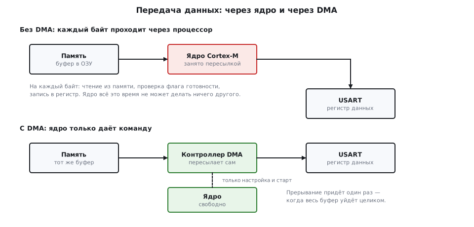
The difference is not only in speed. When transferring through the core, every byte costs a read, a check of the ready flag and a write — and all this in a loop that cannot be left without losing data. When transferring through DMA the interrupt comes once, when the whole buffer has gone out.
Typical tasks where things are bad without DMA:
- receiving and transmitting large packets over UART, SPI, I²C;
- continuous ADC sampling: without DMA some samples will be lost;
- output to a display — there the count is tens of kilobytes per frame;
- generating a signal on the DAC or PWM from a table;
- driving addressable LEDs, where accuracy down to microseconds matters.
Terms used in the documentation
Term Meaning direct memory access transfers done by a controller without the core channel / stream the DMA unit on F1 / on F4 transfer complete the whole transfer is done half transfer half of the buffer has been transferred circular mode the transfer restarts by itself in a circle memory increment the memory address grows after each element peripheral increment the peripheral address grows after each element source / destination where the data is taken from / put to burst transfer several accesses in a row without arbitration FIFO threshold the fill level of the FIFO buffer that triggers a transfer double buffer mode switching between two memory buffers arbiter the block that decides priority between requests update DMA request ( UDE)a DMA request on the timer update event pacing timer a timer that sets the pace of the transfer repetition counter ( RCR)the counter of periods between update events
9.2 Channels on F1, streams on F4
This is one of the most noticeable differences between the platforms. The code does not port at all: both the register names and the model itself differ.
| STM32F1 | STM32F407 | |
|---|---|---|
| unit | channel | stream |
| how many | DMA1 — 7 channels, DMA2 — 5 | DMA1 and DMA2 — 8 streams each |
| source selection | hard-wired: each channel has its own list | stream + selection of one of 8 channels |
| FIFO buffer | no | yes, 4 words |
| burst transfer | no | yes |
| double buffering | no | yes |
| memory ↔ memory | DMA1 and DMA2 can | only DMA2 |
| registers | CCRx, CNDTRx, CPARx, CMARx |
SxCR, SxNDTR, SxPAR, SxM0AR, SxFCR |
| flags | one ISR register for all channels |
LISR for streams 0–3, HISR for 4–7 |
What this means in practice. On F1 you do not choose which channel serves
a peripheral: USART1_TX is always channel 4 of the DMA1 controller, and nothing else.
The mapping table is in the reference manual, and you have to keep it at hand.
Hence the conflicts too: if two peripheral blocks need the same channel, they cannot
work simultaneously.
F4 is more flexible: you choose the stream, and inside it the CHSEL field specifies
whose request it serves. The same USART1_TX is stream 7 of the DMA2 controller,
channel 4.
Where DMA can reach at all. There are several masters on the bus: the core, both DMA controllers, Ethernet, USB HS. They are connected to memory and peripherals by the bus matrix — a set of paths by which a master reaches a slave, and an arbiter that decides who goes first when two ask for the same one. As long as the masters go to different slaves, they work truly simultaneously: DMA moves bytes from the UART to memory, while at the same time the core executes code from Flash.
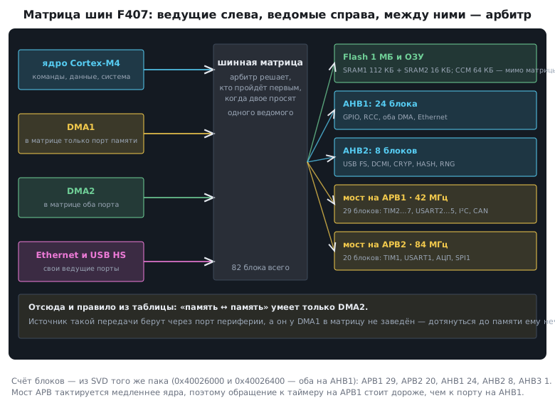
The peripherals hang not on one bus but on five. STM32F407 has 82 blocks — according to the chip description (SVD): 24 on AHB1 (ports, RCC, both DMAs, Ethernet), 8 on AHB2, one on AHB3 and the rest behind two bridges — 29 on APB1 and 20 on APB2. A bridge is needed because APB is clocked more slowly: with the core at 168 MHz APB1 runs at 42 MHz, APB2 at 84 (section 6.6). An access through a bridge costs more: the request goes through an adapter between buses with different frequencies, and the response does not come in the same cycle as with AHB1.
Hence the table row "memory ↔ memory — only DMA2", which otherwise looks arbitrary. The controller takes the source of such a transfer through the peripheral port, and on DMA1 this port is not connected to the matrix — it has no way to reach memory. DMA2 has both ports in the matrix, so it reads from one place in memory and writes to another.
⚠️ Two masters to one slave is a queue, not "simultaneously". If DMA and the core access SRAM at the same time, the arbiter will let one through, and the other will wait a cycle. By eye this is unnoticeable, but when measuring handler time a spread appears that is not in the cycle-count calculation (section 73).
9.3 What has to be set for a transfer
Regardless of the platform, the configuration comes down to five things:
| What | F1 | F4 |
|---|---|---|
| peripheral address | CPAR |
SxPAR |
| memory address | CMAR |
SxM0AR |
| number of elements | CNDTR |
SxNDTR |
| direction | the DIR bit |
the DIR field (two bits) |
| element size and increment | PSIZE, MSIZE, PINC, MINC |
the same names in SxCR |
Increment is the key setting that is confused most often. The memory address
usually has to grow (MINC on), the peripheral address does not: the data register
is always the same. Enable PINC by mistake — and DMA will go and write to the neighbouring
peripheral registers.
Element size is set separately for memory and for the peripheral, and they may differ: for example, storing 16-bit ADC samples into a 16-bit array. A size mismatch is a source of mysterious "shifted" data.
⚠️ The transfer counter is 16-bit. A maximum of 65535 elements per configuration — on both F1 and F4. For more you need circular mode with processing by halves of the buffer.
9.4 Modes
Normal. It transferred NDTR elements, switched off, raised the completion flag.
For a repeated transfer the channel has to be reconfigured.
Circular (CIRC on F1, CIRC on F4). Having counted to the end, the counter
reloads itself and the transfer goes round in a circle. Indispensable for continuous
ADC sampling and audio output: configure it once — it works forever.
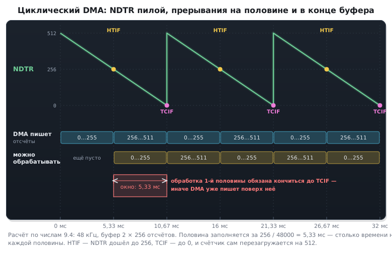
Two interrupts arrive here: half buffer (HTIF) and end of
buffer (TCIF). The technique is this: while DMA fills the second half, you
process the first, and vice versa. The data is not overwritten under your hands
as long as processing one half fits into the time of filling the other: at 48 kHz
and a buffer of 2 × 256 samples this is 5.3 ms. If you do not make it, DMA silently writes over it.
This is classic "poor man's" double buffering, available on F1 too.
Memory to memory. DMA does not necessarily copy faster than memcpy, but the core
is free meanwhile: it computes, serves interrupts or sleeps. F4 has a
limitation: DMA1 cannot do this at all, only DMA2.
Peripheral to peripheral. There is no mode with that name. On F4 the direction is set by
the DIR field in SxCR — two bits, with three values in use: "peripheral → memory"
(0), "memory → peripheral" (1), "memory → memory" (2); on F1 the direction is
the DIR bit in CCRx, and "memory to memory" is a separate MEM2MEM bit. There is no fourth
option in the list, and this is not an omission: it is not needed.
A transfer between two blocks is done as an ordinary "peripheral → memory":
| What to set | Value |
|---|---|
| direction | периферия → память |
| address on the peripheral side | the data register of the source |
| address on the memory side | the data register of the destination |
| address increment | off on both sides: PINC = 0, MINC = 0 |
The controller does not care what is behind an address: for it both are just points on the bus. Hence the increment requirement: a block has one register, there is nowhere to move the pointer, and an enabled increment will move on to the neighbouring register and spoil the configuration of the destination.
This is how, for example, ADC samples are moved straight into the DAC register, or bytes received over SPI into the USART transmitter — without a single processor instruction.
⚠️ Only one side gives the request. A channel is bound to one block — the one whose request it listens to. The other must always be ready: there is no "wait, I am busy" mechanism here, and if the destination did not keep up, the data is silently lost. That is why blocks with obviously different speeds are connected this way: a slow source — a fast destination.
⚠️ Both addresses must be visible from the bus matrix. The CCM memory of the senior F4s is connected straight to the core and not to the matrix (section 2) — it is unsuitable for DMA either as a source or as a destination.
9.5 🔧 Recipe: UART transmission through DMA
STM32F103. USART1_TX is hard-wired to channel 4 of DMA1.
static char tx_buf[64];

void DMA_USART1_TX_Init(void)
{
    RCC->AHBENR |= RCC_AHBENR_DMA1EN;          /* DMA на шине AHB */

    DMA1_Channel4->CCR &= ~DMA_CCR4_EN;        /* настраивать только выключенным */

    DMA1_Channel4->CPAR = (uint32_t)&USART1->DR;
    DMA1_Channel4->CMAR = (uint32_t)tx_buf;
    DMA1_Channel4->CNDTR = 0;

    DMA1_Channel4->CCR = DMA_CCR4_DIR          /* из памяти в периферию */
                       | DMA_CCR4_MINC         /* адрес памяти растёт */
                       | DMA_CCR4_TCIE         /* прерывание по завершении */
                       | DMA_CCR4_PL_1;        /* высокий приоритет */

    NVIC_SetPriority(DMA1_Channel4_IRQn, 6);
    NVIC_EnableIRQ(DMA1_Channel4_IRQn);

    USART1->CR3 |= USART_CR3_DMAT;             /* разрешить запросы от USART */
}

void DMA_USART1_Send(const char *data, uint16_t len)
{
    if (len > sizeof(tx_buf)) {
        len = sizeof(tx_buf);
    }
    while (DMA1_Channel4->CCR & DMA_CCR4_EN) { }   /* прошлая передача ещё идёт */
    memcpy(tx_buf, data, len);

    DMA1_Channel4->CCR &= ~DMA_CCR4_EN;
    DMA1_Channel4->CNDTR = len;
    DMA1_Channel4->CCR |= DMA_CCR4_EN;
}

void DMA1_Channel4_IRQHandler(void)
{
    if (DMA1->ISR & DMA_ISR_TCIF4) {
        DMA1->IFCR = DMA_IFCR_CTCIF4;          /* сброс — в отдельном регистре */
        DMA1_Channel4->CCR &= ~DMA_CCR4_EN;
    }
}
While DMA is sending the buffer, you must not write to it: that is why DMA_USART1_Send first
waits until the TCIF4 handler switches the channel off.
STM32F407. The same USART1_TX is stream 7 of the DMA2 controller, channel 4.
void DMA_USART1_TX_Init(void)
{
    RCC->AHB1ENR |= RCC_AHB1ENR_DMA2EN;

    /* Выключаем поток и ЖДЁМ подтверждения: у F4 бит EN сбрасывается не сразу. */
    DMA2_Stream7->CR &= ~DMA_SxCR_EN;
    while (DMA2_Stream7->CR & DMA_SxCR_EN) { }

    /* Сбрасываем флаги прошлой передачи — иначе новая может не пойти. */
    DMA2->HIFCR = DMA_HIFCR_CTCIF7 | DMA_HIFCR_CHTIF7 | DMA_HIFCR_CTEIF7
                | DMA_HIFCR_CDMEIF7 | DMA_HIFCR_CFEIF7;

    DMA2_Stream7->PAR  = (uint32_t)&USART1->DR;
    DMA2_Stream7->M0AR = (uint32_t)tx_buf;
    DMA2_Stream7->NDTR = 0;

    DMA2_Stream7->CR = (4u << DMA_SxCR_CHSEL_Pos)   /* канал 4 = USART1_TX */
                     | DMA_SxCR_DIR_0               /* 01: память -> периферия */
                     | DMA_SxCR_MINC
                     | DMA_SxCR_TCIE
                     | DMA_SxCR_PL_1;

    DMA2_Stream7->FCR &= ~DMA_SxFCR_DMDIS;          /* прямой режим, без FIFO */

    NVIC_SetPriority(DMA2_Stream7_IRQn, 6);
    NVIC_EnableIRQ(DMA2_Stream7_IRQn);

    USART1->CR3 |= USART_CR3_DMAT;
}
Two differences worth remembering: waiting for EN to clear and mandatory
clearing of the flags before a new transfer. F1 requires neither,
and this is exactly where people stumble when porting.
9.6 The FIFO on F4
Each stream has a 4-word buffer. It lets small portions be collected into large bus accesses: DMA accumulates data and writes it in a batch.
DMA2_Stream7->FCR |= DMA_SxFCR_DMDIS;                 /* включить FIFO */
DMA2_Stream7->FCR |= DMA_SxFCR_FTH;                   /* порог — полный буфер */
When it is needed: at high speeds and with different widths of source and destination — for example, reading memory in words and giving it to the peripheral in bytes.
When it is not needed: for UART at ordinary speeds direct mode (DMDIS = 0) is simpler
and more reliable. A badly chosen threshold gives the FEIF error and silently spoils
the transfer.
Bursts: several words per bus access
With the FIFO enabled a stream can deliver what it has accumulated as a burst — 4, 8 or
16 accesses in a row, without arbitration between them (MBURST for memory,
PBURST for the peripheral). In direct mode bursts are unavailable: the hardware
forces single accesses. The rules whose violation
is paid for with a bus error that is not visible in the DMA registers:
| Rule | Where it comes from |
|---|---|
| burst size × data width no larger than the FIFO threshold: with a ¼ threshold and bytes — only a burst of 4, with a full FIFO and words — also only of 4 | the table of allowed combinations in the controller description |
| the ¾ threshold is forbidden if the peripheral burst exactly fills the FIFO (4 words) | the same place |
| a burst must not cross a 1 KB address boundary | an AHB protocol requirement: the minimum area of one slave is 1 KB |
| accesses inside a burst are aligned to their width | the same place |
HAL checks the first rule itself: HAL_DMA_Init with an incompatible
threshold–burst pair returns the error HAL_DMA_ERROR_PARAM without touching the hardware.
Nobody checks the 1 KB boundary — it is on the conscience of whoever chooses
the buffer address.
The arbiter: who goes first
Each stream has four priority levels in PL (DMA_PRIORITY_LOW …
VERY_HIGH in HAL). If two streams have the same level, the
stream with the lower number wins: stream 2 goes before stream 4. Hence the
practice: give the most demanding source both a high level and a
low stream number, if the channel mapping allows it.
9.7 🔧 PWM from a table: an LED breathes without the processor
DMA writes not only to the data registers of interfaces but to any peripheral
register — for example, to a timer's CCR1. This way the PWM duty cycle is taken from a table:
the LED smoothly brightens and dims, and after configuration the processor sleeps.
There are two timers. The first produces 1 kHz PWM, the second sets the pace: 50 times a second
it sends a DMA request, and DMA moves the next value from the table in a circle
into the first one's CCR1. 100 values at this pace — an inhale and an exhale in 2 s.
| F103 | F407 | |
|---|---|---|
| PWM | TIM3, channel 1: PA6 | TIM4, channel 1: PD12 — the green LED of the Discovery |
| pace | TIM4 | TIM3 |
| request | TIM4_UP — channel 7 of DMA1 | TIM3_UP — stream 2, channel 5 of DMA1 |
The table is round(1000 · pow((1 − cos(2π·i / 100)) / 2, 2.2)): a smooth inhale
along a cosine, raised to the power 2.2 for gamma (57.3), so that the eye sees it as
uniform.
The peak 1000 = ARR + 1 — full brightness at the 50th value. 11 values at the junction
of exhale and inhale are zeros: 0.22 s of darkness between breaths.
static void dma_init(void)
{
#if defined(STM32F10X_MD)
    DMA1_Channel7->CCR   = 0;                                  /* настраивать выключенным */
    DMA1_Channel7->CPAR  = (uint32_t)&PWM->CCR1;               /* куда: регистр другого таймера */
    DMA1_Channel7->CMAR  = (uint32_t)breath;
    DMA1_Channel7->CNDTR = STEPS;
    DMA1_Channel7->CCR   = DMA_CCR7_DIR | DMA_CCR7_MINC | DMA_CCR7_CIRC   /* из памяти, по кругу */
                         | DMA_CCR7_PSIZE_0 | DMA_CCR7_MSIZE_0            /* по 16 бит */
                         | DMA_CCR7_EN;
#elif defined(STM32F407xx)
    DMA1_Stream2->CR &= ~DMA_SxCR_EN;
    while (DMA1_Stream2->CR & DMA_SxCR_EN) { }
    DMA1->LIFCR = DMA_LIFCR_CTCIF2 | DMA_LIFCR_CHTIF2 | DMA_LIFCR_CTEIF2
                | DMA_LIFCR_CDMEIF2 | DMA_LIFCR_CFEIF2;
    DMA1_Stream2->PAR  = (uint32_t)&PWM->CCR1;
    DMA1_Stream2->M0AR = (uint32_t)breath;
    DMA1_Stream2->NDTR = STEPS;
    DMA1_Stream2->CR   = (5u << DMA_SxCR_CHSEL_Pos)            /* канал 5 = TIM3_UP */
                       | DMA_SxCR_DIR_0 | DMA_SxCR_MINC | DMA_SxCR_CIRC
                       | DMA_SxCR_PSIZE_0 | DMA_SxCR_MSIZE_0
                       | DMA_SxCR_EN;
#endif
}

void breath_init(void)
{
    clocks_and_pins();
    dma_init();

    /* ШИМ 1 кГц: новое CCR1 вступает в силу с началом периода */
    PWM->PSC   = PWM_PSC;
    PWM->ARR   = 999u;
    PWM->CCMR1 = TIM_CCMR1_OC1M_2 | TIM_CCMR1_OC1M_1 | TIM_CCMR1_OC1PE;   /* ШИМ 1, предзагрузка */
    PWM->CCER  = TIM_CCER_CC1E;
    PWM->CR1   = TIM_CR1_ARPE;
    PWM->EGR   = TIM_EGR_UG;
    PWM->CR1  |= TIM_CR1_CEN;

    /* темп: 50 раз в секунду запрос DMA, прерывания нет */
    PACE->PSC  = PACE_PSC;                  /* тик 0,1 мс */
    PACE->ARR  = 199u;                      /* 200 тиков — 20 мс */
    PACE->DIER = TIM_DIER_UDE;
    PACE->CR1  = TIM_CR1_CEN;
}

int main(void)
{
    breath_init();
    for (;;)
        __WFI();                            /* спит: таймеры и DMA работают и в Sleep */
}
Why the brightness does not jerk. Thanks to the OC1PE preload DMA writes
to the shadow register, and the PWM picks up the new value at the start of the next
period — there are no shortened pulses (13.4).
It breathes in sleep too. In Sleep the core stands still, but the timers and DMA work (10.2),
so the whole main loop is one __WFI(). In Stop — no: the clocks are stopped there.
And if with an interrupt? The same transfer in a handler is 18 instructions after
armclang with -O2. Interrupt entry and exit cost 12 cycles each
on Cortex-M3 and M4; counting generously two cycles per instruction, we get
24 + 2 × 18 = 60 cycles. At 50 updates per second this is nothing, and even at
10 000 updates per second at 48 MHz it is 10 000 × 60 / 48 000 000 = 1.25 %
of the processor. The gain of DMA here is not in percent: the update does not wait for other
interrupts — no delays, no jitter — and runs while the core sleeps.
One timer instead of two. TIM1 and TIM8 have a repetition counter RCR:
the update event comes once every RCR + 1 periods. With RCR = 19 a 1 kHz PWM
itself requests DMA 1000 / 20 = 50 times a second. Just do not forget MOE (13.5).
9.8 F0 and G0: channels as on F1, DMAMUX on G0
DMA on F0 and G0 is built like F1's, not like F4's: five or seven channels (five —
on F030, F031, G030, G031; seven — on F072, F091, G071), each with
CCR, CNDTR, CPAR, CMAR, and shared ISR and IFCR. There are no streams and no FIFO.
Recipe 9.5 ports almost word for word, but three small things in the names catch you
when porting — and one big one on G0.
The small things. The clock bit on F0 is called DMAEN; the name DMA1EN is kept in the header
as an obsolete alias, and in new code it is better not to mix it
with the main one. The
CCR bits have no channel number: DMA_CCR_DIR, DMA_CCR_MINC, DMA_CCR_TCIE;
code with DMA_CCR4_DIR from the F1 recipe does not build — use of undeclared
identifier 'DMA_CCR4_DIR'. And the USART data register is TDR, not DR
(section 16.9). The interrupts are grouped: on F0 and G0 channel 1 has its own,
channels 2 and 3 share one (DMA1_Channel2_3_IRQn), channels 4–7 share one
among four; on G0 the DMAMUX overrun is added to the last one
(DMA1_Ch4_7_DMAMUX1_OVR_IRQn). In the handler you first look at ISR to see
whose channel it is:
void DMA1_Channel2_3_IRQHandler(void)
{
    if (DMA1->ISR & DMA_ISR_TCIF2) {
        DMA1->IFCR = DMA_IFCR_CTCIF2;
    }
}
Request mapping on F0 is hard-wired, as on F1, only the table is different:
USART1_TX — channel 2, USART1_RX — channel 3; the USART1TX_DMA_RMP bit
in SYSCFG->CFGR1 moves transmission to channel 4, USART1RX_DMA_RMP —
reception to channel 5. The channel configuration is as in 9.5:
    RCC->AHBENR |= RCC_AHBENR_DMAEN;            /* у F0 бит зовётся DMAEN; DMA1EN — устаревший псевдоним */
    DMA1_Channel2->CCR &= ~DMA_CCR_EN;          /* настраивать только выключенным */
    DMA1_Channel2->CPAR = (uint32_t)&USART1->TDR;   /* у нового USART — TDR, не DR */
    DMA1_Channel2->CMAR = (uint32_t)tx_buf;
    DMA1_Channel2->CNDTR = 0;
    DMA1_Channel2->CCR = DMA_CCR_DIR            /* имена битов без номера канала: DMA_CCR_DIR, не DMA_CCR4_DIR */
                       | DMA_CCR_MINC
                       | DMA_CCR_TCIE
                       | DMA_CCR_PL_1;
G0 has no mapping at all — it has DMAMUX. Any request can be routed
to any channel: each DMA channel has its own multiplexer channel with
a single CCR register, into which the request number is written. The numbers are in the LL header
stm32g0xx_ll_dmamux.h: USART1_TX — 51, USART2_TX — 53, ADC1 — 5,
memory-to-memory — 0. The numbering is offset: DMA channel 1 is DMAMUX channel 0.
Without a write to DMAMUX the channel is configured correctly, enabled — and silent: the request
does not reach it. This is the most frequent mistake when porting from F0 and F1:
    /* канал 1 DMA1 — это канал 0 DMAMUX: нумерация со сдвигом на единицу */
    DMAMUX1_Channel0->CCR = LL_DMAMUX_REQ_USART2_TX;    /* без этой строки канал молчит */
    DMA1_Channel1->CCR &= ~DMA_CCR_EN;
    DMA1_Channel1->CPAR = (uint32_t)&USART2->TDR;
After that everything is as on F0: CMAR, CNDTR, CCR, DMAT in the USART. On the other hand, G0
has no mapping table with its conflicts of "two needed requests on one
channel" — any peripheral gets any free channel.
9.9 Pitfalls
Configuring with the channel enabled. Writes to the address and counter registers
with EN set are ignored. On F4 it is not enough to clear the bit — you must wait
until the hardware confirms it.
Uncleared flags. On F4 a new transfer may not start if flags of the previous one remain. Clear them before the start, not after.
A forgotten enable on the peripheral side. DMA itself is configured correctly, but
USART_CR3_DMAT, ADC_CR2_DMA or SPI_CR2_TXDMAEN are not enabled — there are simply
no requests, and the transfer does not go. No diagnostics at all.
Through HAL: the exchange is "stuck" in BUSY. HAL_UART_Transmit_DMA returned
HAL_OK, the data went out, but the next call answers HAL_BUSY. In HAL
the state returns to READY not at the end of DMA but on the TC interrupt
of the USART itself: the DMA handler only clears DMAT and sets TCIE. You need
both interrupts in the NVIC — the DMA stream's and the USART's; the absence of either of them
leaves gState = BUSY_TX forever. Reception in Normal mode after
RxCpltCallback does not restart by itself: HAL clears DMAR and waits for a new
HAL_UART_Receive_DMA; only Circular continues without a call.
Through HAL: the I²C buffer interrupt with DMA. In DMA mode HAL enables
only ITEVTEN and ITERREN; it leaves ITBUFEN to the interrupt modes without DMA.
An ITBUFEN set by hand will make the event handler parse the bytes
that DMA is already moving.
A buffer in CCM. The senior F4s have 64 KB of fast memory connected straight
to the core. It is inaccessible to the DMA controller: a buffer placed there will not
be transferred — the stream immediately switches off with the error flag TEIFx. If this flag is not
looked at, there will be silence. Keep DMA buffers in ordinary SRAM.
A local buffer. An array declared inside a function lives on the stack and disappears on exit. DMA will keep writing to its address even after other data has appeared there. Make DMA buffers static or global.
Missing volatile. The data that DMA brings changes outside of
the code — as with interrupts. Without volatile the compiler is entitled
to cache the value (the analysis with assembly is in section 3).
The data cache on F7 and H7. On Cortex-M7 the core works with memory through a cache,
and DMA works directly with RAM, and volatile does not help here: the core reads
a stale copy of the received buffer from the cache, and what the core wrote may not reach RAM by
the start of the transfer. Before transmission the buffer is pushed out to RAM
(SCB_CleanDCache_by_Addr), after reception it is discarded from the cache
(SCB_InvalidateDCache_by_Addr), the buffer itself is aligned and made a multiple of
32 bytes — a cache line; or the buffers are put into a region that the MPU marks
as non-cacheable (section 124.6).
Channel conflict on F1. Two peripheral blocks mapped to the same channel will not work simultaneously. Check against the mapping table beforehand, not after "SPI broke the ADC".
Alignment. If an element is 16- or 32-bit, the buffer addresses must be
aligned accordingly. A uint8_t array cast to uint16_t*
may give a transfer error.
DMA to a timer is silent. The update request is enabled by the UDE bit
in the DIER of the pacing timer. Without it the DMA channel is configured correctly, but there are no transfers —
as with DMAT on the UART.
The element size does not match the table. A uint16_t table with a 32-bit MSIZE
is read in words: DMA takes every second value and runs
past the end of the table. MSIZE follows the element size in memory, PSIZE the register.
9.10 Summary
- DMA frees the core: the interrupt comes once for the whole buffer, not for every byte.
- F1 has channels with hard-wired peripheral mapping, F4 has streams with channel selection, FIFO, burst and double buffering. Code does not port between the platforms.
- The configuration is the peripheral address, the memory address, the count, the direction,
the sizes and the increments.
MINCis on,PINCusually is not. - The counter is 16-bit: a maximum of 65535 elements per configuration.
- Circular mode plus half- and end-of-buffer interrupts give a continuous stream without data loss.
- Configure only with the channel disabled; on F4 wait for confirmation that
ENis cleared and clear the flags of the previous transfer. - Do not forget to enable requests on the peripheral side (
DMAT,DMA,TXDMAEN). - Buffers are static, in ordinary SRAM (not in CCM), aligned,
volatile; on F7 and H7 there is also cache handling: clean before transmission, invalidate after reception. - DMA writes to any peripheral register: table → a timer's
CCRon the request of another timer (UDE) gives PWM from a table without the processor, including in sleep.
Full sources
dma_f0.c — DMA on STM32F072: USART1_TX on channel 2.
/* Раздел 9.8: DMA на STM32F072 — как у F1: каналы, USART1_TX на канале 2
 * (перенос на канал 4 — бит USART1TX_DMA_RMP в SYSCFG). */
#include <stddef.h>
#include "stm32f0xx.h"

_Static_assert(offsetof(DMA_Channel_TypeDef, CNDTR) == 0x04u && offsetof(DMA_Channel_TypeDef, CMAR) == 0x0Cu,
               "регистры канала — как у F1");
_Static_assert(offsetof(DMA_TypeDef, IFCR) == 0x04u, "ISR и IFCR");

static char tx_buf[64];

void dma_usart1_tx_init_f0(void)
{
    RCC->AHBENR |= RCC_AHBENR_DMAEN;            /* у F0 бит зовётся DMAEN; DMA1EN — устаревший псевдоним */
    DMA1_Channel2->CCR &= ~DMA_CCR_EN;          /* настраивать только выключенным */
    DMA1_Channel2->CPAR = (uint32_t)&USART1->TDR;   /* у нового USART — TDR, не DR */
    DMA1_Channel2->CMAR = (uint32_t)tx_buf;
    DMA1_Channel2->CNDTR = 0;
    DMA1_Channel2->CCR = DMA_CCR_DIR            /* имена битов без номера канала: DMA_CCR_DIR, не DMA_CCR4_DIR */
                       | DMA_CCR_MINC
                       | DMA_CCR_TCIE
                       | DMA_CCR_PL_1;
    NVIC_SetPriority(DMA1_Channel2_3_IRQn, 2);  /* у F0 одно прерывание на каналы 2 и 3 */
    NVIC_EnableIRQ(DMA1_Channel2_3_IRQn);
    USART1->CR3 |= USART_CR3_DMAT;
}

void dma_usart1_send_f0(const char *data, uint16_t len)
{
    for (uint16_t i = 0; i < len && i < sizeof tx_buf; i++)
        tx_buf[i] = data[i];
    DMA1_Channel2->CCR &= ~DMA_CCR_EN;
    DMA1_Channel2->CNDTR = len;
    DMA1_Channel2->CCR |= DMA_CCR_EN;
}

void DMA1_Channel2_3_IRQHandler(void)
{
    if (DMA1->ISR & DMA_ISR_TCIF2) {
        DMA1->IFCR = DMA_IFCR_CTCIF2;
    }
}
dma_g0.c — DMA on STM32G071: the USART2_TX request through DMAMUX.
/* Раздел 9.8: DMA на STM32G071 — те же каналы, но запрос к каналу подводит DMAMUX:
 * USART2_TX на канале 1 DMA1 через DMAMUX1_Channel0. */
#include <stddef.h>
#include "stm32g0xx.h"
#include "stm32g0xx_ll_dmamux.h"

_Static_assert(offsetof(DMA_Channel_TypeDef, CMAR) == 0x0Cu, "регистры канала — как у F0 и F1");
_Static_assert(LL_DMAMUX_REQ_USART2_TX == 53u && LL_DMAMUX_REQ_USART1_TX == 51u && LL_DMAMUX_REQ_ADC1 == 5u,
               "номера запросов DMAMUX из LL");
_Static_assert(offsetof(DMAMUX_Channel_TypeDef, CCR) == 0u, "у канала DMAMUX один регистр CCR");

static char tx_buf[64];

void dma_usart2_tx_init_g0(void)
{
    RCC->AHBENR |= RCC_AHBENR_DMA1EN;
    /* канал 1 DMA1 — это канал 0 DMAMUX: нумерация со сдвигом на единицу */
    DMAMUX1_Channel0->CCR = LL_DMAMUX_REQ_USART2_TX;    /* без этой строки канал молчит */
    DMA1_Channel1->CCR &= ~DMA_CCR_EN;
    DMA1_Channel1->CPAR = (uint32_t)&USART2->TDR;
    DMA1_Channel1->CMAR = (uint32_t)tx_buf;
    DMA1_Channel1->CNDTR = 0;
    DMA1_Channel1->CCR = DMA_CCR_DIR | DMA_CCR_MINC | DMA_CCR_TCIE | DMA_CCR_PL_1;
    NVIC_SetPriority(DMA1_Channel1_IRQn, 2);
    NVIC_EnableIRQ(DMA1_Channel1_IRQn);
    USART2->CR3 |= USART_CR3_DMAT;
}

void dma_usart2_send_g0(const char *data, uint16_t len)
{
    for (uint16_t i = 0; i < len && i < sizeof tx_buf; i++)
        tx_buf[i] = data[i];
    DMA1_Channel1->CCR &= ~DMA_CCR_EN;
    DMA1_Channel1->CNDTR = len;
    DMA1_Channel1->CCR |= DMA_CCR_EN;
}

void DMA1_Channel1_IRQHandler(void)
{
    if (DMA1->ISR & DMA_ISR_TCIF1) {
        DMA1->IFCR = DMA_IFCR_CTCIF1;
    }
}
Next: section 9а "GPDMA on STM32U5: linked lists, triggers and ring reception without interrupts" —
on U5, instead of the CIRC bit and a mapping table, there is a chain of transfer descriptions in memory.