 Embedded HandbookApps
8. Input/output ports (GPIO)
GPIO (General-Purpose Input/Output) is how the microcontroller touches the outside world. Everything else — timers, UART, SPI — ultimately goes out through the same pins. That is why GPIO is studied first: without understanding it you cannot even light an LED.
Ports are named by letters: GPIOA, GPIOB, GPIOC… Each port has up to 16 pins,
and each pin is configured independently of its neighbours.
How many are there? The number of pins depends on the package (LQFP48, BGA176…), the family (F0, F1, F4…) and on whether pins are taken by the HSE/LSE crystals.
8.1 How it works
The structure of one pin
Any STM32 pin is not a "leg" but a small circuit: a pair of protection diodes, pull-up and pull-down resistors, a Schmitt trigger at the input, a pair of transistors at the output and multiplexers that decide who controls the pin — your code or a peripheral.
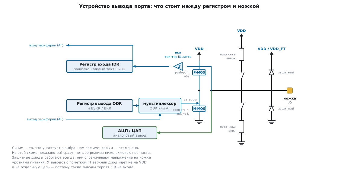 Basic structure of an I/O port pin
5 V tolerance. In the diagram the protection diode is marked VDD_FT.
It means that the pin tolerates a 5 V input signal with the MCU powered from 3.3 V. If the datasheet
has no such marking for a pin, you must not apply more than the supply (the typical margin
is only ~0.3 V). Pins routed to the ADC are usually not tolerant. And a tolerant
pin has two caveats: it tolerates 5 V only with the supply present — the limit is
VDD + 4 V, so 5 V must not be applied to an unpowered chip; and above
VDD + 0.3 V its internal pull resistors must be off. On F4 the tolerance
also disappears in analog mode.
How much current a pin handles. The absolute limit on F1 and F4 is 25 mA per pin,
sunk or sourced, but the datasheet guarantees the 0 and 1 levels only up to 8 mA
(up to 20 mA — with degraded levels). The sum of the currents of all pins together with the consumption of the
chip itself is no more than 150 mA on F103 and 240 mA on F407, separately through VDD and through
VSS. PC13–PC15 — no more than 3 mA and not as a current source (section 2.6).
An LED is connected through a resistor: (3.3 − 2.0) V / 330 Ω ≈ 4 mA; a relay,
a motor and a long LED strip — only through a transistor.
Eight pin modes
Terms used in the documentation
Term Meaning port bit configuration the settings of one port pin output push-pull an output that drives both high and low output open-drain an output that only pulls low floating input an input with no pull resistor input with pull-up / pull-down an input pulled to the supply / to ground Schmitt trigger an input stage with hysteresis output driving current the current an output can supply maximum output speed the edge rate setting of an output five-volt tolerant ( FT)a pin that accepts 5 V alternate function a pin driven by a peripheral atomic bit set/reset setting and clearing a bit in one bus write locking mechanism freezing the configuration until reset
| Mode | What it does |
|---|---|
| Input floating | input, pull resistors off (the state after reset) |
| Input pull-up | input, pulled to the supply |
| Input pull-down | input, pulled to ground |
| Analog | ADC input/DAC output; the digital circuitry is off |
| Output push-pull | a "push-pull" output: 1 → VDD, 0 → GND |
| Output open-drain | an open-drain output: 0 → GND, 1 → Hi-Z |
| AF push-pull | the pin is driven by a peripheral, push-pull output |
| AF open-drain | the pin is driven by a peripheral, open-drain output |
What happens to the hardware in each mode is shown in the figures below:
Input — the output buffer is off, the Schmitt trigger is on, pull resistors as configured,
the pin state is latched into IDR on every bus cycle.
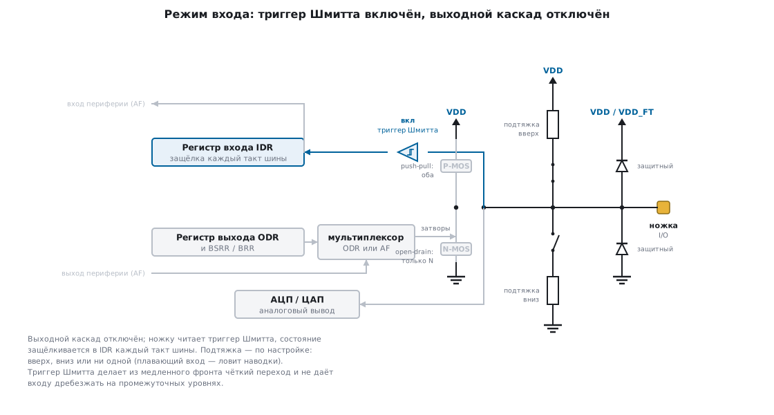 Input: floating, pulled up/down
Output — the output buffer works; reading IDR gives the real level on the pin,
reading ODR gives the last value written. The difference matters: in open-drain mode
an external circuit can "overpower" it, and the pin will not have what you wrote.
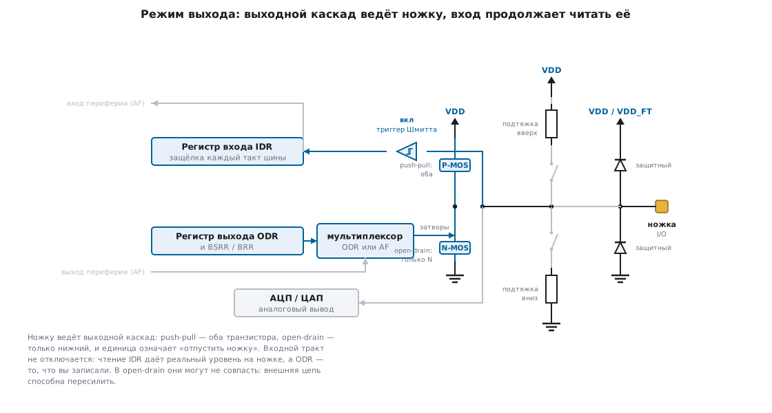 Output
Alternate function — the buffer is controlled by a signal from a peripheral (USART, SPI, I²C). If you configure a pin as AF but do not enable the peripheral itself, the output state is undefined.
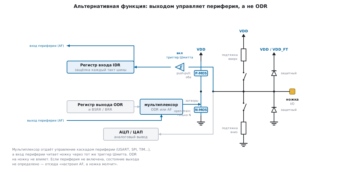 Alternate function
Analog — the output buffer is off, the Schmitt trigger is off (otherwise it
would draw current at intermediate levels), pull resistors are off, reading IDR gives 0.
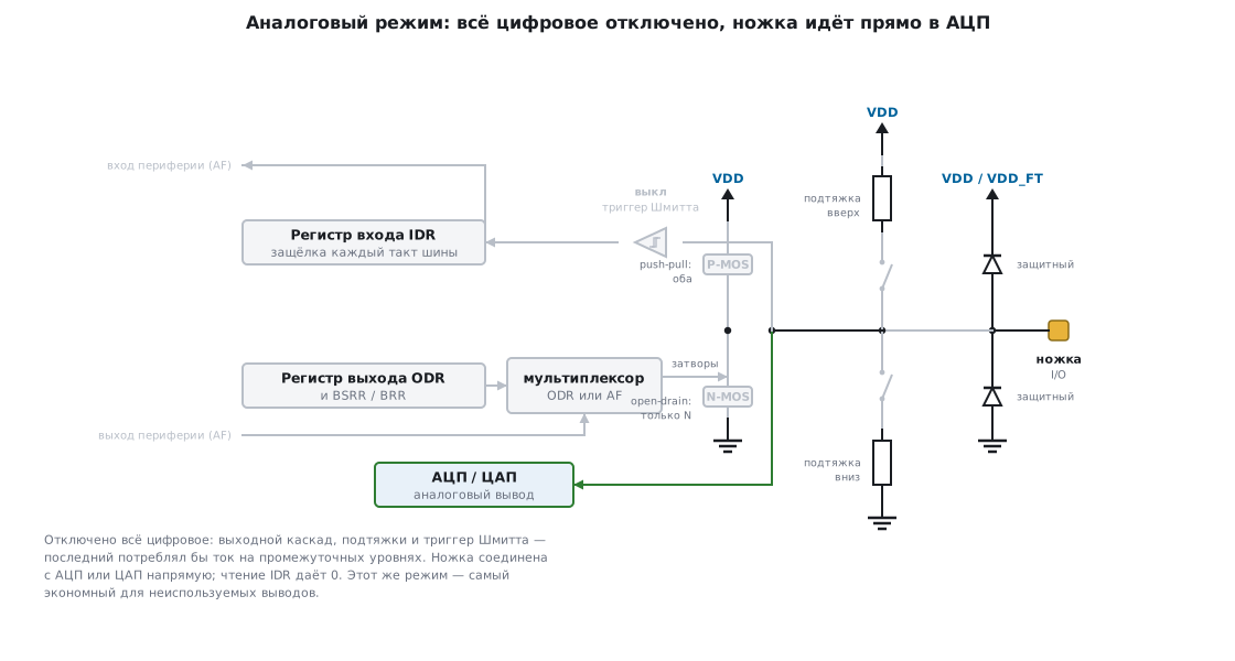 High-impedance analog input
Atomic access
The classic mistake is to change the pin state through ODR:
GPIOC->ODR |= (1 << 13); // читать → изменить → записать: ТРИ операции
An interrupt can come or an RTOS task can switch between the read and the write —
and a neighbouring bit changed there will be lost. That is why GPIO has separate registers
BSRR and BRR: a write to them changes the selected ODR bits in a single bus operation,
leaving the others untouched.
8.2 Registers
⚠️ The main fork of the whole section. STM32F1 and all the other families (F0, F3, F4, F7, L0, L4, G0, G4, H7…) have different GPIO register layouts. Code with
MODERwill not build for F1, code withCRL/CRHwill not build for F4. When you meet examples that contradict each other, look not at "correctness" but at which generation of peripherals they were written for.
| What we configure | STM32F1 | Other families |
|---|---|---|
| pin mode | CRL / CRH — 4 bits each (MODE[1:0]+CNF[1:0]) |
MODER — 2 bits each |
| push-pull / open-drain | in the same place, in CNF |
OTYPER |
| edge rate | in the same place, in MODE |
OSPEEDR |
| pull resistors | CNF=10 + a bit in ODR |
PUPDR |
| alternate function number | none (only a coarse remap through AFIO_MAPR) |
AFRL / AFRH |
| read / write | IDR / ODR |
the same |
| atomic set | BSRR / BRR |
BSRR (BRR is not everywhere) |
STM32F1 registers
| Register | Offset | After reset | Purpose |
|---|---|---|---|
GPIOx_CRL |
0x00 | 0x4444 4444 |
configuration of pins 0–7 |
GPIOx_CRH |
0x04 | 0x4444 4444 |
configuration of pins 8–15 |
GPIOx_IDR |
0x08 | 0x0000 XXXX |
input data, read-only |
GPIOx_ODR |
0x0C | 0x0000 0000 |
output data |
GPIOx_BSRR |
0x10 | 0x0000 0000 |
atomic: set (BS) / reset (BR) |
GPIOx_BRR |
0x14 | 0x0000 0000 |
atomic: reset only |
GPIOx_LCKR |
0x18 | 0x0000 0000 |
configuration lock until MCU reset |
The reset value 0x44444444 means CNF=01, MODE=00 for every pin —
that is, after reset all pins are floating inputs.
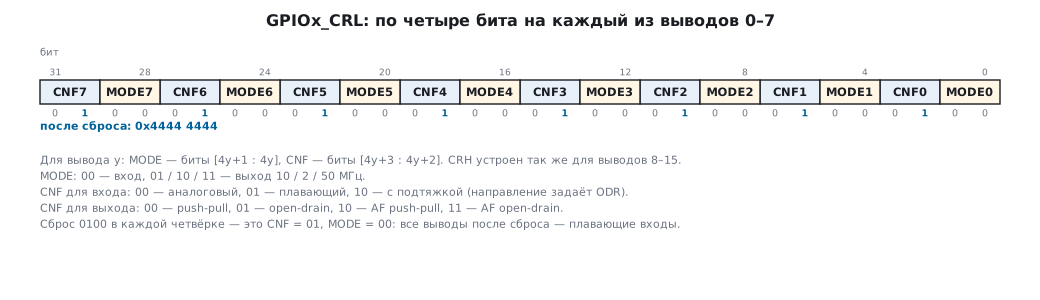 Bits of the
GPIOx_CRL register, ports x=A..G
4 bits per pin. For pin y: bits [4y+1:4y] are MODE, bits [4y+3:4y+2] are CNF.
MODE[1:0] — input or output, and at what speed:
MODE |
Value |
|---|---|
00 |
input (after reset) |
01 |
output, maximum 10 MHz |
10 |
output, maximum 2 MHz |
11 |
output, maximum 50 MHz |
CNF[1:0] is read differently depending on MODE:
CNF |
if MODE=00 (input) |
if MODE≠00 (output) |
|---|---|---|
00 |
analog | push-pull |
01 |
floating input (after reset) | open-drain |
10 |
input with pull | AF push-pull |
11 |
reserved | AF open-drain |
⚠️ A little-known detail. In input-with-pull mode (
CNF=10) the direction of the pull is set not by a separate register but by a bit inODR: 1 — up, 0 — down. If you configuredCNF=10and forgot aboutODR, you get a pull-down, although the code says not a word about it. F4 and the others have an honestPUPDRfor this.
Speed is not "the faster the better". The setting limits the edge steepness. Setting 50 MHz where an LED blinks means needlessly raising the electromagnetic interference from the board. For slow signals take 2 MHz.
BSRR and BRR
BSRR is 32 bits: the lower 16 (BS0..BS15) set ODR bits, the upper 16
(BR0..BR15) reset them. If both BS and BR are set for the same pin, BS wins.
BRR — reset only, the lower 16 bits.
Both registers are write-only, reading returns zeros.
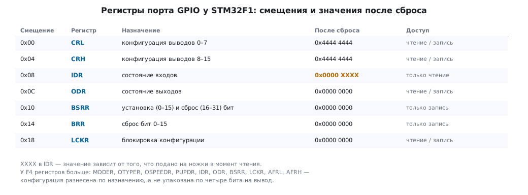 GPIO register map and reset values
Configuration lock (LCKR)
Lets you "freeze" the pin configuration until the next MCU reset — protection against
someone else's code accidentally reconfiguring a critical pin. It requires a strict
sequence of writes of the LCKK key (bit 16): write 1 → write 0 →
write 1 → read 0 → read 1. Any deviation cancels the lock.
What is taken right after reset
The pins of the JTAG/SWD debug interface come up not floating but in their own modes:
PA15 (JTDI, pull-up), PA14 (JTCK, pull-down), PA13 (JTMS, pull-up),
PB4 (JNTRST, pull-up).
⚠️ By taking
PA13/PA14for your own needs, you lose SWD — and with it the ability to reflash the board the usual way. Hence the commented-out lines withAFIO_MAPR_SWJ_CFG_JTAGDISABLEin the button example below: they are enabled deliberately and only when you are really short of pins.
STM32F4 registers
On F4 the same peripheral is designed in a fundamentally different way: instead of two registers with
4-bit fields — five separate registers, each with its own meaning. This is more convenient:
change the speed — you touch only OSPEEDR, without risking the mode.
| Register | Offset | Bits per pin | Purpose |
|---|---|---|---|
MODER |
0x00 | 2 | mode: input / output / alternate function / analog |
OTYPER |
0x04 | 1 | 0 — push-pull, 1 — open-drain |
OSPEEDR |
0x08 | 2 | edge rate: low / medium / high / very high |
PUPDR |
0x0C | 2 | 00 — none, 01 — up, 10 — down |
IDR |
0x10 | 1 | input data, read-only |
ODR |
0x14 | 1 | output data |
BSRR |
0x18 | 1 | atomic set (BS) and reset (BR) |
LCKR |
0x1C | 1 | configuration lock |
AFR[0], AFR[1] |
0x20, 0x24 | 4 | alternate function number AF0…AF15 |
MODER, two-bit fields:
MODER |
Mode |
|---|---|
00 |
input (after reset, except the SWD pins) |
01 |
general-purpose output |
10 |
alternate function |
11 |
analog |
Three differences that keep F1 code from porting to F4:
- The ports are on a different bus. On F1 the clock is enabled in
RCC->APB2ENR(IOPxEN), on F4 inRCC->AHB1ENR(GPIOxEN). Copied the line withAPB2ENR— the port is silent. - Different base addresses.
GPIOAon F1 is0x4001 0800, on F40x4002 0000, the step between ports is0x400. TheODRoffset on F1 is0x0C, on F40x14. - Alternate functions for real. On F4 each pin can get any
of the sixteen alternate functions through
AFR[0](pins 0–7) andAFR[1](8–15), 4 bits per pin. F1 has no such register at all — there is only a coarse "remap" with ready-made combinations throughAFIO_MAPR. This is perhaps the most noticeable improvement of F4 for board layout: a peripheral can be put on almost any pins.
/* Назначить PA9 функцию AF7 (USART1_TX) — так это делается только у F4 */
GPIOA->MODER  &= ~GPIO_MODER_MODER9;
GPIOA->MODER  |=  GPIO_MODER_MODER9_1;          /* 10 -> альтернативная функция */
GPIOA->AFR[1] &= ~GPIO_AFRH_AFSEL9;             /* вывод 9 -> AFR[1], биты 7:4 */
GPIOA->AFR[1] |=  (7u << GPIO_AFRH_AFSEL9_Pos); /* AF7 */
⚠️ The alternate function number is not universal: AF7 is USART1/2/3 on F407, but on another chip the same number may carry a different peripheral. Look up the alternate function table in the datasheet of the specific MCU (not in the reference manual — it is not there).
8.3 HAL, LL and CubeMX
HAL hides the differences between families behind one structure.
typedef struct {
  uint32_t Pin;        // маска выводов: GPIO_PIN_5, или GPIO_PIN_1|GPIO_PIN_5
  uint32_t Mode;       // GPIO_MODE_OUTPUT_PP, GPIO_MODE_INPUT, ...
  uint32_t Pull;       // GPIO_NOPULL | GPIO_PULLUP | GPIO_PULLDOWN
  uint32_t Speed;      // GPIO_SPEED_FREQ_LOW ... _VERY_HIGH
  uint32_t Alternate;  // номер альтернативной функции
} GPIO_InitTypeDef;
Pinis a mask, not a number:GPIO_PIN_5equals0x0020, not 5. TheAlternatefield does not exist in CubeF1 — F1 has noAFRL/AFRHregisters, the remap is done throughAFIO_MAPR.
The Mode values, besides the obvious ones, include interrupt and event modes:
GPIO_MODE_IT_RISING, GPIO_MODE_IT_FALLING, GPIO_MODE_IT_RISING_FALLING
(covered in section 7 on EXTI) and GPIO_MODE_EVT_* — waking the core by
the WFE instruction without calling a handler.
Five functions for all work with a pin:
GPIO_PinState HAL_GPIO_ReadPin (GPIO_TypeDef *GPIOx, uint16_t Pin);
void          HAL_GPIO_WritePin(GPIO_TypeDef *GPIOx, uint16_t Pin, GPIO_PinState St);
void          HAL_GPIO_TogglePin(GPIO_TypeDef *GPIOx, uint16_t Pin);
HAL_StatusTypeDef HAL_GPIO_LockPin(GPIO_TypeDef *GPIOx, uint16_t Pin);
void          HAL_GPIO_DeInit  (GPIO_TypeDef *GPIOx, uint32_t Pin);
ReadPin returns GPIO_PIN_RESET or GPIO_PIN_SET. DeInit returns the pin
to its reset state (floating input) — useful before going to sleep, so as not
to waste current.
The same thing in three ways — turn on PA5:
/* регистры, F1 */          GPIOA->BSRR = GPIO_BSRR_BS5;
/* LL */                    LL_GPIO_SetOutputPin(GPIOA, LL_GPIO_PIN_5);
/* HAL */                   HAL_GPIO_WritePin(GPIOA, GPIO_PIN_5, GPIO_PIN_SET);
All three compile into a write to BSRR. HAL adds a function call, LL an
inline wrapper. The choice is a matter of readability and portability, not speed.
8.4 🔧 Recipe: blinking an LED
A BluePill board (STM32F103C8T6), an LED on PC13.
#include "stm32f10x.h"

void PORTC_13_INIT (void)
{
    RCC->APB2ENR |= RCC_APB2ENR_IOPCEN;      // такт на порт C — без него порт мёртв

    GPIOC->CRH &= ~GPIO_CRH_MODE13;          // сброс MODE13
    GPIOC->CRH |=  GPIO_CRH_MODE13_1;        // MODE13 = 10 -> выход 2 МГц
    GPIOC->CRH &= ~GPIO_CRH_CNF13;           // CNF13  = 00 -> push-pull
}

int main (void)
{
    PORTC_13_INIT();

    while (1)
    {
        GPIOC->BSRR = GPIO_BSRR_BR13;        // зажечь: светодиод включён катодом

        for (volatile int i = 0; i < 1000000; i++) { }

        GPIOC->BSRR = GPIO_BSRR_BS13;        // погасить

        for (volatile int i = 0; i < 1000000; i++) { }
    }
}
Walkthrough:
PC13is a pin of the upper half of the port, henceCRH, notCRL.- The port clock is enabled always and separately, even if the core is already clocked
at 72 MHz. Forgetting
RCC->APB2ENRis the most frequent cause of "the code is right, but the pin is silent". IOPCENstands for Input/Output Port C ENable.- A delay with an empty loop is a placeholder: a real one comes from SysTick or a timer (sections 7 and 13).
The counter is declared
volatile: without it the optimiser will throw out the empty loop entirely (section 3.4), and instead of blinking the LED will glow at half brightness.
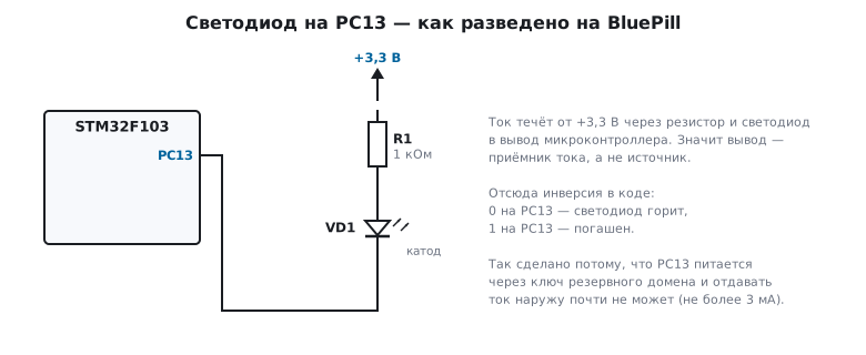
⚠️ The BluePill LED lights on zero.
PC13is connected to the cathode:BR13(a zero at the output) turns it on,BS13turns it off. AndBSRRis a write-only register, so it is written with=, not|=: reading gives 0, and|=only adds an unnecessary bus access.
The same with HAL:
__HAL_RCC_GPIOC_CLK_ENABLE();

GPIO_InitTypeDef g = {0};
g.Pin   = GPIO_PIN_13;
g.Mode  = GPIO_MODE_OUTPUT_PP;
g.Pull  = GPIO_NOPULL;
g.Speed = GPIO_SPEED_FREQ_LOW;
HAL_GPIO_Init(GPIOC, &g);

while (1) {
    HAL_GPIO_TogglePin(GPIOC, GPIO_PIN_13);
    HAL_Delay(500);
}
The same on STM32F4 — Discovery F407, the green LED LD4 on PD12:
#include "stm32f4xx.h"

void PD12_INIT(void)
{
    RCC->AHB1ENR |= RCC_AHB1ENR_GPIODEN;        /* AHB1, а не APB2 */

    GPIOD->MODER   &= ~GPIO_MODER_MODER12;
    GPIOD->MODER   |=  GPIO_MODER_MODER12_0;    /* 01 -> выход */
    GPIOD->OTYPER  &= ~GPIO_OTYPER_OT12;        /* push-pull */
    GPIOD->OSPEEDR &= ~GPIO_OSPEEDR_OSPEED12;   /* низкая скорость */
    GPIOD->PUPDR   &= ~GPIO_PUPDR_PUPD12;       /* без подтяжек */
}

int main(void)
{
    PD12_INIT();

    while (1)
    {
        GPIOD->BSRR = GPIO_BSRR_BS12;           /* только запись, без |= */
        for (volatile int i = 0; i < 1000000; i++) { }
        GPIOD->BSRR = GPIO_BSRR_BR12;
        for (volatile int i = 0; i < 1000000; i++) { }
    }
}
On Nucleo-F401RE/F411RE the LED LD2 sits on PA5 — only the port and the pin number
change, the structure of the code is the same.
Compare with the F1 version above: five separate registers instead of CRH, AHB1ENR
instead of APB2ENR. The logic is identical — enable the clock, set the mode, write
to BSRR. This is the practical meaning of the "core versus peripherals" split
from section 1.
8.5 🔧 Recipe: polling a button
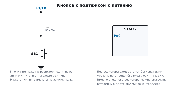
A button on PA0, an LED on PB2.
uint32_t Button_State = 0;

#define LED_PB2_ON()   (GPIOB->BSRR = GPIO_BSRR_BS2)
#define LED_PB2_OFF()  (GPIOB->BSRR = GPIO_BSRR_BR2)

void PINA_0_INIT (void)                      // кнопка PA0
{
    RCC->APB2ENR |= RCC_APB2ENR_IOPAEN;

    GPIOA->CRL &= ~GPIO_CRL_MODE0_0;         // MODE0 = 00 -> вход
    GPIOA->CRL &= ~GPIO_CRL_MODE0_1;

    GPIOA->CRL |=  GPIO_CRL_CNF0_0;          // CNF0 = 01 -> плавающий вход:
    GPIOA->CRL &= ~GPIO_CRL_CNF0_1;          // подтяжка стоит на плате
}

void PINB_2_INIT (void)                      // светодиод PB2
{
    RCC->APB2ENR |= RCC_APB2ENR_IOPBEN;

    GPIOB->CRL &= ~GPIO_CRL_MODE2_0;         // MODE2 = 10 -> выход 2 МГц
    GPIOB->CRL |=  GPIO_CRL_MODE2_1;

    GPIOB->CRL &= ~GPIO_CRL_CNF2_0;          // CNF2 = 00 -> push-pull
    GPIOB->CRL &= ~GPIO_CRL_CNF2_1;
}

int main (void)
{
    PINB_2_INIT();
    PINA_0_INIT();

//  SET_BIT(RCC->APB2ENR, RCC_APB2ENR_AFIOEN);
//  CLEAR_BIT(AFIO->MAPR, AFIO_MAPR_SWJ_CFG);
//  SET_BIT(AFIO->MAPR, AFIO_MAPR_SWJ_CFG_JTAGDISABLE);

    while (1)
    {
        Button_State = READ_BIT(GPIOA->IDR, GPIO_IDR_IDR0);

        if (Button_State == 1)
            {
             LED_PB2_ON();
            }
        else
            {
               LED_PB2_OFF();
            }
    }
}
⚠️
READ_BITreturns a mask, not a one. Here the comparison with1works only becauseGPIO_IDR_IDR0equals0x0001. Move the button toPA5— andREAD_BITwill return0x0020, the condition== 1will never be met, and the code will look correct. And do not put the mask into auint8_t: for pins 8–15 it will be truncated to zero, and even!= 0will not work — that is whyButton_Stateis 32-bit here. This is more reliable:
c
if (READ_BIT(GPIOA->IDR, GPIO_IDR_IDR5) != 0) { ... }
⚠️ A floating input under a button holds an undefined level while the button is not pressed — the pin picks up noise. A pull is needed: an external resistor or
CNF0 = 10plus the corresponding bit inODR(see the pitfall in 8.2).
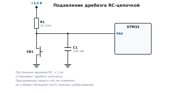
Bounce. A mechanical contact gives a burst of pulses on press and release lasting from one to tens of milliseconds. In a polling loop this shows up as multiple triggering. The cure is a software delay after the first edge, latching the state on two matching readings 10–20 ms apart, or an RC network on the board:
Handling a button on an interrupt — section 7 (EXTI).
8.6 F0 and G0: registers as on F4, plus BRR
The F0 and G0 ports are built like F4's: MODER, OTYPER, OSPEEDR, PUPDR,
AFR, and BSRR at the same offset 0x18. On top there is a BRR register
at 0x28 — resetting a pin by writing a one, separately from BSRR. There are three differences,
and each breaks code porting:
| F0 | G0 | |
|---|---|---|
| port clock | RCC->AHBENR |
RCC->IOPENR |
port A MODER after reset |
0x28000000 — inputs |
0xEBFFFFFF — analog |
| bit names | GPIO_MODER_MODER5, GPIO_BSRR_BS_5, GPIO_IDR_0 |
GPIO_MODER_MODE5, GPIO_BSRR_BS5, GPIO_IDR_ID0 |
The reset values come from the peripheral description files (SVD) in the packs. On port B
of G0 MODER after reset is 0xFFFFFFFF: all pins are analog.
On G0 an input must be enabled explicitly. Analog mode (MODER = 11) saves
current, but the digital input is off in it — IDR reads zero whatever is
on the pin. F4 code that relied on "after reset it is an input" sees
the button always pressed on G0:
RCC->IOPENR |= RCC_IOPENR_GPIOAEN;                          /* порты у G0 — регистр IOPENR */
GPIOA->MODER = (GPIOA->MODER & ~GPIO_MODER_MODE5) | GPIO_MODER_MODE5_0;     /* 01 — выход */
GPIOA->MODER &= ~GPIO_MODER_MODE0;                          /* 00 — вход: после сброса там 11 */
GPIOA->PUPDR |= GPIO_PUPDR_PUPD0_0;
The bit names are different. The G0 header names the fields in a new way, and code for F0 does not build with it: "use of undeclared identifier 'GPIO_MODER_MODER5'". The same LED on F0:
RCC->AHBENR |= RCC_AHBENR_GPIOAEN;                          /* порты у F0 — на шине AHB */
GPIOA->MODER = (GPIOA->MODER & ~GPIO_MODER_MODER5) | GPIO_MODER_MODER5_0;   /* 01 — выход */
GPIOA->BSRR = GPIO_BSRR_BS_5;
GPIOA->BRR = GPIO_BRR_BR_5;                                 /* то же, что BSRR = BR_5 */
The portable way is not the names of individual bits but masks by pin number
(3u << (2u * pin) for MODER) or the LL library: its functions are named
the same on both series.
8.7 The same pin on 1986VE9x
The same tasks on the Russian Cortex-M3 from Milandr are solved identically in meaning:
enable the port clock, set the mode, write to the data register. What differs is
the register names and the fact that a pin is configured not by a MODE/CNF pair
but by separate registers OE, FUNC, ANALOG, PULL, PWR.
The practical value here is not in the API differences but in the fact that the line of reasoning carries over between different Cortex-M cores unchanged.
8.8 Exercises
Eight LEDs LED1..LED8 on the pins of one BluePill port. Every step
of any exercise is one write to ODR or BSRR, without reading the port.
- "Running light": one LED, from left to right.
- A "running light" of three LEDs in a row.
- "Accumulation" from left to right: they light up one by one and stay on.
- "Collapse": pairs from the edges converge to the middle in turn (
LED1+LED8,LED2+LED7, …), then go out in the reverse order.
One more — on logical expressions: implement an output
whose state equals a logical function of two buttons (AND, OR, exclusive OR),
without using branches — only bit operations on IDR and BSRR.
8.9 Pitfalls
An example with MODER does not build for F1, an example with CRL does not build for F4. GPIO on F1 and on the other families
are built differently (8.2).
An input with pull pulls down, although not a word is said about it. On F1 the pull direction is set by a bit in ODR (8.2).
After "freeing" PA13/PA14 the board cannot be flashed. The SWD pins were given to something else — disable JTAG/SWD
only deliberately (8.2).
The wrong alternate function. The AF number means different things on different chips; the table is in the datasheet of the specific chip (8.2).
The BluePill LED lights the other way round. It is connected with its cathode to PC13: BS13 turns it off, BR13 turns it on (8.4).
A button on another pin stopped being read. READ_BIT returned a mask and the code compared it with 1 — or the mask was put into a uint8_t, and for pins 8–15 it was truncated to zero (8.5).
The button "presses" itself. A floating input without a pull picks up noise (8.5).
8.10 Summary
- A port does not work until its clock is enabled in
RCC. - After reset all pins are floating inputs,
CRL/CRH=0x44444444. - Change the output state through
BSRR/BRR, not throughODR. - On F1 the configuration is in
CRL/CRH(4 bits per pin), on the other families inMODER+OTYPER+OSPEEDR+PUPDR. Code does not port between them without changes. - Pin speed is about electromagnetic compatibility, not performance.
PA13/PA14are taken by SWD; by freeing them you lose debugging.
Full sources
gpio_f0.c — LED PA5 and button PA0 on STM32F072.
/* Раздел 8.6: светодиод PA5 и кнопка PA0 на STM32F072.
 * Регистры — как у F4 (MODER, OTYPER, OSPEEDR, PUPDR) плюс BRR; такт портов — на AHB. */
#include <stddef.h>
#include "stm32f0xx.h"

_Static_assert(offsetof(GPIO_TypeDef, MODER) == 0x00u && offsetof(GPIO_TypeDef, BSRR) == 0x18u, "как у F4");
_Static_assert(offsetof(GPIO_TypeDef, BRR) == 0x28u, "BRR — сброс вывода записью единицы, у F4 его нет");

void led_init_f0(void)
{
    RCC->AHBENR |= RCC_AHBENR_GPIOAEN;                          /* порты у F0 — на шине AHB */
    GPIOA->MODER = (GPIOA->MODER & ~GPIO_MODER_MODER5) | GPIO_MODER_MODER5_0;   /* 01 — выход */
    GPIOA->PUPDR |= GPIO_PUPDR_PUPDR0_0;                        /* PA0 — вход с подтяжкой вверх */
}

void led_on_f0(void)
{
    GPIOA->BSRR = GPIO_BSRR_BS_5;
}

void led_off_f0(void)
{
    GPIOA->BRR = GPIO_BRR_BR_5;                                 /* то же, что BSRR = BR_5 */
}

uint32_t button_f0(void)
{
    return (GPIOA->IDR & GPIO_IDR_0) == 0u;                     /* нажата — вывод на земле */
}
gpio_g0.c — the same on STM32G071: after reset the input is analog, it is enabled explicitly.
/* Раздел 8.6: светодиод PA5 и кнопка PA0 на STM32G071.
 * После сброса выводы G0 — аналоговые (MODER = 11): вход надо включить явно. */
#include <stddef.h>
#include "stm32g0xx.h"

_Static_assert(offsetof(GPIO_TypeDef, BRR) == 0x28u, "BRR на том же месте, что у F0");

void led_init_g0(void)
{
    RCC->IOPENR |= RCC_IOPENR_GPIOAEN;                          /* порты у G0 — регистр IOPENR */
    GPIOA->MODER = (GPIOA->MODER & ~GPIO_MODER_MODE5) | GPIO_MODER_MODE5_0;     /* 01 — выход */
    GPIOA->MODER &= ~GPIO_MODER_MODE0;                          /* 00 — вход: после сброса там 11 */
    GPIOA->PUPDR |= GPIO_PUPDR_PUPD0_0;
}

void led_on_g0(void)
{
    GPIOA->BSRR = GPIO_BSRR_BS5;
}

void led_off_g0(void)
{
    GPIOA->BRR = GPIO_BRR_BR5;
}

uint32_t button_g0(void)
{
    return (GPIOA->IDR & GPIO_IDR_ID0) == 0u;
}
Next: section 9 "Direct memory access (DMA)".