 Embedded HandbookApps
173а. Power loss: how many milliseconds you have, PVD and BOR, what to save in time
Subsection 10.7 puts it briefly: the voltage detector gives a warning, and the program has time to save its data. This section covers exactly how much time it has, where to get the warning earlier, what can be written at all in those milliseconds, and how to make sure that what was saved survives a thousand pulled plugs. Section 173 protected the board input against reverse polarity and surges; this one protects against an ordinary power-off.
All the times below come from an ngspice model and from the F103 and F407 datasheet tables; the PVD handler and the BOR setup were built with armclang, and the journal with interruptions was run on a PC.
Terms used in the documentation
Term Meaning programmable voltage detector (PVD) a detector with a programmable voltage threshold power-on / power-down reset (POR/PDR) reset at power-up / at power-down brownout reset (BOR) reset when the supply sags hold-up time how long the circuit lives after the input is lost bulk capacitor an energy-storage capacitor supercapacitor a very large capacitor (supercap, ultracapacitor) backup domain / backup registers the backup domain / registers kept in it backup SRAM backup RAM option bytes configuration bytes in Flash torn write a write cut off halfway
173а.1 How much time you have
While the input is present, the bus capacitors are charged to the working voltage. When the input is gone, the load keeps drawing its current and the voltage falls. For a linear regulator and for the chip itself the load is an almost constant current, and the time takes one line to compute:
t = C · ΔU / I,
where ΔU runs from the threshold at which the program learned about the trouble down to the lower limit
of the chip's supply. For the F103 the lower limit is 2.0 V (table 9 of the datasheet). The PVD threshold
named PWR_CR_PLS_2V9 on the falling edge is 2.78 V typical and 2.66 V worst case
(table 11). So ΔU = 0.78 V, and a safe calculation uses 0.66 V.
A 3.3 V bus, a 25 mA load:
| Capacitance on the bus | Typical (0.78 V) | Worst-case threshold (0.66 V) |
|---|---|---|
| 10 µF | 0.312 ms | 0.264 ms |
| 100 µF | 3.12 ms | 2.64 ms |
| 470 µF | 14.7 ms | 12.4 ms |
| 1000 µF | 31.2 ms | 26.4 ms |
A typical training board holds about ten microfarads on the 3.3 V bus, which is a quarter of a millisecond. Writing one eight-byte record to F103 Flash takes 0.28 ms in the worst case (173а.4), so on a bare board it may not fit.
For a switching regulator the formula is different: it draws constant power from the input, not constant current, and the capacitor gives up energy:
t = C · (U₁² − U₂²) / (2P).
The same 470 µF on a 12 V input, from 9.0 V down to 4.5 V, with P = 3.3 V · 25 mA / 0.85 = 0.097 W, gives 147 ms; a linear regulator from the same 9.0 V down to 4.3 V would last 73.6 ms. The switching regulator makes better use of the high voltage: the lower the input, the more current it asks for, but there is still plenty of energy in the capacitor.
173а.2 Where to catch it: the internal PVD or a comparator on the input
The PVD watches the chip's own VDD, that is, the regulator output. As long as the regulator holds 3.3 V, the PVD stays silent, even though the input has been falling for a long time. The warning comes when there is almost no margin left.
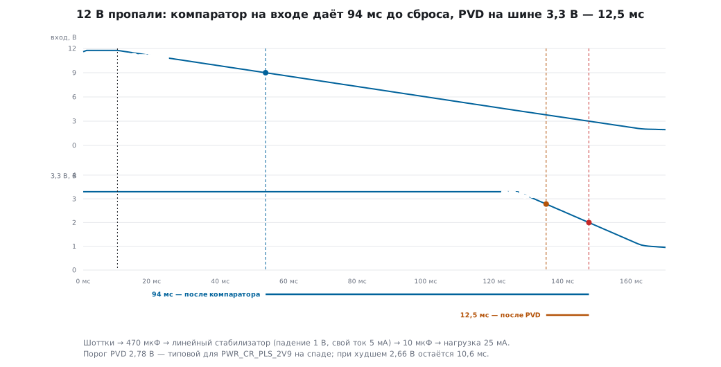
The model: 12 V through a Schottky diode charges 470 µF on the input, followed by a linear regulator (1 V dropout, 5 mA quiescent current), 10 µF on the output and a 25 mA load. The source disappears at the 10th millisecond:
| Where to catch it | 470 µF on the input | 10 µF on the input |
|---|---|---|
| comparator on the input, 9 V threshold | 94.4 ms | 2.43 ms |
| PVD, 2.78 V (typical) | 12.5 ms | 0.52 ms |
| PVD, 2.66 V (worst-case threshold) | 10.6 ms | 0.44 ms |
The difference is 7.5 times with a large capacitor and 4.7 times with a small one. The gain comes not from any cleverness of the comparator but from the voltage: from 9 V down to 4.3 V the capacitor gives up 4.7 V worth of charge, while in the PVD window it gives up 0.78 V.
The threshold on the input is set with a divider. 100 kΩ and 22 kΩ turn 9.0 V into 1.623 V; for the F103 ADC with a 3.3 V reference that is code 2014. The ADC analog watchdog (section 14) raises an interrupt as soon as the channel drops below this code, and at that moment the reference is still an honest 3.3 V, because the regulator is still holding. A plain GPIO input with a divider will not do for this: its threshold wanders between 0.35 and 0.65 VDD.
The internal PVD is still worth enabling, as a second line of defense. It catches what the input cannot see: a sag from the board's own overload, a disconnection after the regulator, power from USB that bypasses the input.
173а.3 BOR: the reset that does not let the chip run at the edge
The detector only warns. If the supply keeps falling, the chip must stop in time rather than run at a voltage at which Flash is read with errors.
The F103 has only POR/PDR: reset on the falling edge at 1.88 V typical (1.8–1.96 V),
on the rising edge at 1.92 V (1.84–2.0 V). The lower supply limit is 2.0 V.
Between the reset threshold and 2.0 V lies a band where the chip is no longer required to work
correctly but has not been reset yet: the core may execute garbage instead of an instruction. If
Flash is unlocked at that moment, a random write lands anywhere. Hence two
rules: keep Flash locked (FLASH_CR_LOCK) all the time except during the
write itself, and where a failure is costly, add an external supply supervisor, a reset
chip with a threshold of, say, 2.9 V. The same band causes trouble when the supply rises slowly
from a supercapacitor or a solar panel: the chip starts at 1.92 V, drops out
at the first current surge, starts again — the reset bouncing from 61.3.
The F407 has a real BOR with three levels in the option bytes:
BOR_LEV bits |
Level | Falling, V (min/typ/max) | Rising, typ, V |
|---|---|---|---|
| 11 | off: POR/PDR applies | 1.60 / 1.68 / 1.76 | 1.72 |
| 10 | 1 | 2.13 / 2.19 / 2.24 | 2.29 |
| 01 | 2 | 2.44 / 2.50 / 2.56 | 2.59 |
| 00 | 3 | 2.75 / 2.83 / 2.88 | 2.92 |
From the factory BOR is off (bits 11). Yet writing to F407 Flash in 32-bit words
(PSIZE = x32, which is what HAL uses for the 2.7–3.6 V range) is allowed only from
2.7 V; half-words from 2.1 V, bytes from 1.8 V. If the firmware writes Flash
in words, set BOR to level 3: then the chip resets before the supply
drops below 2.7 V:
void bor_level3(void)
{
    if ((FLASH->OPTCR & FLASH_OPTCR_BOR_LEV) == 0) return;   /* уже 00 — уровень 3 */
    FLASH->OPTKEYR = 0x08192A3Bu;
    FLASH->OPTKEYR = 0x4C5D6E7Fu;
    FLASH->OPTCR &= ~FLASH_OPTCR_BOR_LEV;     /* 00 — уровень 3: спад 2,75…2,88 В */
    FLASH->OPTCR |= FLASH_OPTCR_OPTSTRT;
    while (FLASH->SR & FLASH_SR_BSY) { }
    FLASH->OPTCR |= FLASH_OPTCR_OPTLOCK;
}
The option bytes are rewritten once: the check in the first line prevents erasing them at every power-up.
173а.4 What to save in time
The budget is a few milliseconds or a few tens of milliseconds. The Flash tables from the datasheets:
| Operation | F103 | F407 |
|---|---|---|
| erase | 1 KB page: 20–40 ms | 16 KB sector (x32): 250–500 ms, 128 KB: 1–2 s |
| write 8 bytes | 4 half-words × 40–70 µs = 0.16–0.28 ms | 2 words (x32) × 16–100 µs = 0.032–0.2 ms |
| write and erase current | up to 5 mA above normal | 12 mA (x32, 3.3 V) |
| backup registers | 10 × 16 bits = 20 bytes | 20 × 32 bits = 80 bytes |
| backup SRAM | none | 4 KB |
There is one conclusion from the table: you cannot erase at the moment of power loss. An F103 page takes longer to erase than even a board with 470 µF stays alive, and an F407 sector takes tens of times longer. You can only write to a place erased in advance, which is why in 11.8 and 42.6 data is written as a journal: a new record is appended to a clean slot, and the old one stays. The page is erased later, at normal supply, when the journal has filled up.
The PVD handler for the F103 appends one slot of four half-words: the data, the check value and the marker, with the marker last:
void pvd_init(void)
{
    RCC->APB1ENR |= RCC_APB1ENR_PWREN;
    PWR->CR = (PWR->CR & ~PWR_CR_PLS) | PWR_CR_PLS_2V9 | PWR_CR_PVDE;   /* спад: 2,66…2,90 В */
    EXTI->IMR  |= EXTI_IMR_MR16;
    EXTI->RTSR |= EXTI_RTSR_TR16;       /* PVDO = 1, когда питание НИЖЕ порога */
    NVIC_SetPriority(PVD_IRQn, 0);
    NVIC_EnableIRQ(PVD_IRQn);
}

void PVD_IRQHandler(void)
{
    EXTI->PR = EXTI_PR_PR16;
    GPIOB->BSRR = GPIO_BSRR_BR12;       /* снять нагрузку: подсветку, радио, реле */
    uint32_t v = counter;
    if (next_slot + 8u <= LOG_END) {    /* страница кончилась — стирать некогда */
        FLASH->KEYR = 0x45670123u;
        FLASH->KEYR = 0xCDEF89ABu;
        flash_write16(next_slot + 2u, (uint16_t)v);
        flash_write16(next_slot + 4u, (uint16_t)(v >> 16));
        flash_write16(next_slot + 6u, (uint16_t)~(v ^ (v >> 16)));   /* контроль */
        flash_write16(next_slot, REC_MAGIC);                        /* метка — последней */
        FLASH->CR |= FLASH_CR_LOCK;
        next_slot += 8u;
    }
    while (PWR->CSR & PWR_CSR_PVDO) { } /* был провал, а не отключение: ждём возврата */
    NVIC_SystemReset();
}
Three details. The EXTI16 interrupt is set to the rising edge: the PVDO flag
becomes one when the supply drops below the threshold. The priority is the highest:
the handler must not wait for someone else to finish. And the handler
does not hang forever: if the supply has come back (it was a dip, not a power-off), the
chip restarts and keeps working.
Backup registers and backup SRAM are three orders of magnitude faster than Flash: a write takes clock cycles, not microseconds. But they survive only while there is power on the VBAT pin. On the F103 without a battery on VBAT the backup domain is powered from VDD and loses everything together with it. On the F407 the 4 KB of backup SRAM are kept by a separate low-power regulator, which you enable explicitly:
void bkpsram_on(void)
{
    RCC->APB1ENR |= RCC_APB1ENR_PWREN;
    PWR->CR |= PWR_CR_DBP;                    /* снять защиту резервного домена */
    RCC->AHB1ENR |= RCC_AHB1ENR_BKPSRAMEN;
    PWR->CSR |= PWR_CSR_BRE;                  /* резервный стабилизатор: 4 КБ живут на VBAT */
    while (!(PWR->CSR & PWR_CSR_BRR)) { }
}
With a battery on VBAT, the "last words" — the reason, a counter, the time — are written to backup SRAM even with a budget of half a millisecond, and moved to Flash after the next power-up, when there is all the time in the world.
173а.5 Stored energy and shedding load
If the budget is not enough, you have two levers: add energy or reduce the current.
A capacitor at high voltage and behind a diode. For a linear regulator what counts is the charge C · ΔU, and the same capacitor on the 12 V input gives 7.5 times more time than on the 3.3 V bus (173а.2). The diode in front of it (section 169, 169.6) is mandatory: without it the capacitor gives its charge back into the wire and into every other load on the same line. A large capacitor on the input draws an inrush current at power-up; limit it as in 172.5.
A supercapacitor when you need seconds. 0.1 F on the 3.3 V bus behind a Schottky diode (about 0.3 V drop) holds the chip from the PVD trip down to 2.0 V for about 3 s at 25 mA. Charge it through a resistor: 33 Ω with an empty supercapacitor gives an inrush of 100 mA, and it charges in five time constants, 5 · 33 Ω · 0.1 F = 16.5 s. A diode in parallel with the resistor lets the discharge current bypass it. Until it is fully charged the device must not count on the reserve: measure the supercapacitor voltage with the ADC and allow writes only above a threshold.
Shed the load first. The backlight, the radio module, a relay, a motor draw more than the chip. The first line of the PVD handler switches them off, and the hold-up time grows by the same factor as the current falls. Also switch to a low frequency: the core at 8 MHz from HSI draws several times less than at 72 MHz. But switching the frequency also takes time, and the Flash wait states must be adjusted (section 6), so first switch off the external loads, then write.
173а.6 Testing: a thousand interruptions
A torn write cannot be checked by eye: most of the time everything works, and once in a hundred power-offs the data turns into garbage. You test it with numbers.
On a PC. A model of an F103 Flash page: an erased half-word is 0xFFFF, a write
can only clear bits, an erase sets them; an interrupted operation leaves
each bit that was supposed to change in a half state, changed or not.
A thousand interruptions at a random moment during saving, two methods:
| Method | Duration | New | Old | Garbage |
|---|---|---|---|---|
| erase the page and write the value | 40.14 ms | 0 | 0 | 1000 |
| append to the journal: data, check, marker | 0.28 ms | 3 | 997 | 0 |
The naive method corrupts the data at every interruption: the erase is long, and the interruption almost always falls on it. The journal never returned garbage: the reader finds either the new record or the previous one. The three "new" results are cases where the marker managed to land completely exactly at the moment of interruption, with the data already written before it. Here the interruption is in the middle of the write itself, the worst case; if the write starts on the PVD signal and fits into the budget, the journal saves the new value every time.
On the bench. The model does not know everything about real Flash, so the product is tested with power-offs: a second board controls a switch in the supply of the board under test (section 171), turns it off at a random time after each write and turns it back on a second later. After start-up the board under test checks the journal and sends the number of the last intact record over UART; the second board counts how many times the number went back by more than one record and how many times the journal turned out to be corrupted. A thousand cycles of two seconds each is a little over half an hour. Disconnect the debugger during the test: the ST-Link powers the board through its 3.3 V pin, and the power-off is no longer real.
173а.7 Pitfalls
- Erasing a page in the PVD handler. Erasing an F103 page takes up to 40 ms, an F407 sector up to 500 ms for 16 KB. The budget will never be enough; the page is left half-erased, and both the old and the new data are lost.
- Taking the threshold name for the threshold.
PWR_CR_PLS_2V9on the falling edge trips at 2.66–2.90 V, 2.78 V typical. Compute the budget for the worst case, 2.66 V. - Falling edge on EXTI16. The
PVDOflag is one when the supply is below the threshold. ConfiguringFTSRmeans getting the interrupt when power returns, when there is nothing left to save. - The handler hangs in an empty loop. A 20 ms dip does not switch the chip off:
power has come back, but the firmware sits in
for (;;)until a manual reset. Wait forPVDO = 0and restart. - A capacitor without a diode. The charge goes into neighboring loads and into the wiring; the calculated milliseconds turn into fractions of a millisecond.
- F407 BOR left off. The chip runs down to 1.7 V, while writes in 32-bit words are allowed only from 2.7 V. Set level 3 in the option bytes.
- Backup registers without a battery. Without VBAT the F103 backup domain is powered from VDD and forgets everything together with it.
- Testing with the debugger connected. The ST-Link keeps the board alive through its 3.3 V pin; switching off the source switches nothing off.
173а.8 Summary
- Hold-up time for a linear regulator is t = C · ΔU / I, for a switching one t = C · (U₁² − U₂²) / (2P). On a 3.3 V bus at 25 mA, 10 µF give 0.264 ms and 470 µF give 12.4 ms at the worst-case PVD threshold.
PWR_CR_PLS_2V9on the F103 is 2.66–2.90 V on the falling edge; the lower supply limit is 2.0 V. A comparator on the 12 V input with 470 µF gives 94.4 ms, the PVD gives 12.5 ms.- The F103 has only POR/PDR (falling at 1.88 V), the F407 has a three-level BOR, off from the factory; 32-bit writes to F407 Flash are allowed only from 2.7 V.
- At the moment of power loss Flash is only appended to, in a place erased in advance: an erase takes 20–40 ms on the F103 and hundreds of milliseconds on the F407, writing 8 bytes takes up to 0.28 ms.
- Backup registers and backup SRAM are fast, but only with a battery on VBAT.
- A thousand interruptions in the middle of saving: "erase and write" gives garbage 1000 times, the journal with the marker written last gives it not once.
Full sources
pvd173a_f1.c — F103: PVD on EXTI16 and the "last words" in a page erased in advance.
/* 173а: F103 — PVD на EXTI16 и «последние слова» в заранее стёртую страницу Flash.
   Собирается armclang против stm32f10x.h пака Keil (проверка _verify/pwr173a_check.py). */
#include <stdint.h>

#define LOG_PAGE   0x0800FC00u          /* последняя страница 64 КБ, стёрта заранее */
#define LOG_END    (LOG_PAGE + 1024u)
#define REC_MAGIC  0xA55Au

volatile uint32_t counter;              /* то, что жалко потерять */
static uint32_t next_slot = LOG_PAGE;   /* первый чистый слот, ищется при старте */

void pvd_init(void)
{
    RCC->APB1ENR |= RCC_APB1ENR_PWREN;
    PWR->CR = (PWR->CR & ~PWR_CR_PLS) | PWR_CR_PLS_2V9 | PWR_CR_PVDE;   /* спад: 2,66…2,90 В */
    EXTI->IMR  |= EXTI_IMR_MR16;
    EXTI->RTSR |= EXTI_RTSR_TR16;       /* PVDO = 1, когда питание НИЖЕ порога */
    NVIC_SetPriority(PVD_IRQn, 0);
    NVIC_EnableIRQ(PVD_IRQn);
}

static void flash_write16(uint32_t addr, uint16_t v)
{
    FLASH->CR |= FLASH_CR_PG;
    *(volatile uint16_t *)addr = v;
    while (FLASH->SR & FLASH_SR_BSY) { }
    FLASH->CR &= ~FLASH_CR_PG;
}

void PVD_IRQHandler(void)
{
    EXTI->PR = EXTI_PR_PR16;
    GPIOB->BSRR = GPIO_BSRR_BR12;       /* снять нагрузку: подсветку, радио, реле */
    uint32_t v = counter;
    if (next_slot + 8u <= LOG_END) {    /* страница кончилась — стирать некогда */
        FLASH->KEYR = 0x45670123u;
        FLASH->KEYR = 0xCDEF89ABu;
        flash_write16(next_slot + 2u, (uint16_t)v);
        flash_write16(next_slot + 4u, (uint16_t)(v >> 16));
        flash_write16(next_slot + 6u, (uint16_t)~(v ^ (v >> 16)));   /* контроль */
        flash_write16(next_slot, REC_MAGIC);                        /* метка — последней */
        FLASH->CR |= FLASH_CR_LOCK;
        next_slot += 8u;
    }
    while (PWR->CSR & PWR_CSR_PVDO) { } /* был провал, а не отключение: ждём возврата */
    NVIC_SystemReset();
}
bor173a_f4.c — F407: the BOR level in the option bytes and backup SRAM on a battery.
/* 173а: F407 — уровень BOR в байтах конфигурации и резервное ОЗУ на батарейке.
   Собирается armclang против stm32f4xx.h пака Keil (проверка _verify/pwr173a_check.py). */
#include <stdint.h>

void bor_level3(void)
{
    if ((FLASH->OPTCR & FLASH_OPTCR_BOR_LEV) == 0) return;   /* уже 00 — уровень 3 */
    FLASH->OPTKEYR = 0x08192A3Bu;
    FLASH->OPTKEYR = 0x4C5D6E7Fu;
    FLASH->OPTCR &= ~FLASH_OPTCR_BOR_LEV;     /* 00 — уровень 3: спад 2,75…2,88 В */
    FLASH->OPTCR |= FLASH_OPTCR_OPTSTRT;
    while (FLASH->SR & FLASH_SR_BSY) { }
    FLASH->OPTCR |= FLASH_OPTCR_OPTLOCK;
}

void bkpsram_on(void)
{
    RCC->APB1ENR |= RCC_APB1ENR_PWREN;
    PWR->CR |= PWR_CR_DBP;                    /* снять защиту резервного домена */
    RCC->AHB1ENR |= RCC_AHB1ENR_BKPSRAMEN;
    PWR->CSR |= PWR_CSR_BRE;                  /* резервный стабилизатор: 4 КБ живут на VBAT */
    while (!(PWR->CSR & PWR_CSR_BRR)) { }
}

#define LAST_WORDS ((volatile uint32_t *)BKPSRAM_BASE)

void last_words(uint32_t counter, uint32_t reason)
{
    LAST_WORDS[1] = counter;                  /* запись в ОЗУ — такты, не миллисекунды */
    LAST_WORDS[2] = reason;
    LAST_WORDS[0] = 0x5AFEC0DEu;              /* метка — последней */
}
Next: section 173б "Li-ion on the board: charging, protection and how much is left" — how to charge the board from a single lithium cell, take care of it and know how much charge is left.