 Embedded HandbookApps
173б. Li-ion on the board: charging, protection and how much is left
Section 173 protected the board input, 173а counted the milliseconds after the supply was lost. Here the power source is carried along: a single lithium cell. The board needs three things from it: to charge, not to damage the cell, and to know how much is left. Ready-made chips do the first two; the third is most often done by the microcontroller, and that is where most of the mistakes are: a divider that is off by hundreds of millivolts, an ADC reference that sags together with the battery, and a current counter that drifts by several percent in a day.
What this section relies on: the cell model is the same as in section 121 (an open-circuit table
of 3.00…4.20 V in 11 points, R0 = 0.05 Ω, R1·C1 = 0.03 Ω · 1000 F, 2.5 Ah);
the 4.2 V charge voltage is a well-known constant of this chemistry. What a
charge controller must know comes from the bindings and drivers of charger chips
in the Zephyr v4.4.2 tree (section 34а). Pin leakage currents, VREFINT and the
absolute maximum ratings come from the F103 (DocID13587) and G474 (DS12288) datasheets in the
Keil packs. Everything is computed by a model on a PC in the stm-lab:1 image, directory
_verify/liion173c; the conversion code was built with armclang for the G474 and checked against the
model on the PC. The datasheets of specific charger chips and protection boards
are not used here, and their thresholds are not given.
Terms used in the documentation
Term Meaning constant current / constant voltage (CC/CV) charging with a constant current, then a constant voltage precharge, trickle charge pre-charging with a small current charge termination current the current at which charging ends re-charge voltage the voltage below which charging starts again protection circuit (overcharge, overdischarge, overcurrent) cell protection against overcharge, overdischarge, overload open-circuit voltage (OCV) the voltage with no load state of charge (SoC) charge as a fraction of full capacity coulomb counting, fuel gauge integrating the current, a charge meter input leakage current (Ilkg) the current that leaks through an input dropout voltage the input-output difference of a regulator
173б.1 The cell and what is known about it in advance
For the firmware the cell is the circuit from section 121: a source of an open-circuit voltage that depends on the charge, a series resistance R0 and an RC network. Under current the terminal voltage differs from the open-circuit one by I·R0 and by the voltage of the network, which settles with a time constant of R1·C1 = 30 s.
This circuit immediately gives three numbers that the whole section rests on.
4.2 V is the charge limit (a well-known constant for this chemistry; other lithium chemistries have their own). You must not charge above it, and it is the charger chip, not the program, that holds this limit.
4.2 V is above the absolute maximum supply voltage. On both the F103 and the G474 the limit
for VDD is 4.0 V (on the G474 it also covers VDDA, VBAT and VREF+). The cell
is never connected straight to the chip supply: there is a regulator between them
(173б.6).
The open-circuit table is flat. Between 30 and 50 % charge the voltage rises by only 0.5 V over the full scale, which is 0.20 % of charge per millivolt; near the bottom end (0…10 %) it is nine times steeper, 4.5 V per scale. Anything that adds about ten millivolts to the voltage measurement means, in the middle of the scale, several percent of charge.
173б.2 CC/CV charging
Charging goes in two stages. First a constant current, until the voltage at the terminals reaches 4.2 V. Then 4.2 V is held constant and the current falls by itself; when it drops to the termination current, charging is switched off. A deeply discharged cell is first brought up with a small current, the precharge; the model does not show it.
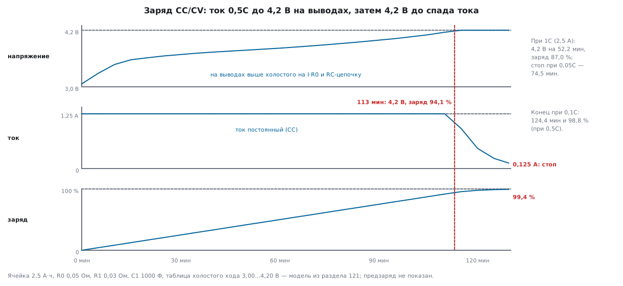
The model is the cell from 121, starting from zero charge:
| Charge current | 4.2 V at the terminals | Charge at that moment | End at 0.1C | End at 0.05C |
|---|---|---|---|---|
| 0.5C = 1.25 A | 113.0 min | 94.1 % | 124.4 min, 98.8 % | 129.4 min, 99.4 % |
| 1C = 2.5 A | 52.2 min | 87.0 % | 69.5 min, 98.8 % | 74.5 min, 99.4 % |
What it shows.
The cell is not full when the terminals reach 4.2 V. At 1.25 A the terminals are above the open-circuit voltage by I·R0 and by the RC network, and 4.2 V is reached at 94.1 % charge; at 2.5 A already at 87.0 %. The constant-voltage stage adds the rest.
Twice the current does not mean twice as fast. The constant-current stage is more than twice shorter (113.0 → 52.2 min), but the constant-voltage stage is longer: 11.4 → 17.3 min to 0.1C.
The final charge is set by the termination current, not by the charge current. At 0.1C both charges end at 98.8 %, at 0.05C at 99.4 %: at the end the current is small, and the terminals are above the open-circuit voltage only by that current times R0 + R1.
The 0.5C and 1C currents and the termination current here are examples for the model. The real limits for a cell are in its datasheet, and in a charger chip they are set with resistors or registers.
173б.3 The charger chip and cell protection
What a charge controller must know about the cell is clearly seen in the Zephyr battery
description (dts/bindings/battery/battery.yaml): the precharge current,
the charge termination current, the maximum constant current, the maximum
constant voltage, the re-charge voltage, the capacity and an
open-circuit table of 11 points, from 0 to 100 % in steps of 10 %, exactly as in
the model from 121. And what the chip reports about itself is seen in the Zephyr charger
programming interface (include/zephyr/drivers/charger.h):
| What | States in charger.h |
|---|---|
| is it charging | charging, not charging, full |
| at what current | precharge (TRICKLE), fast (FAST), standard, gentle (LONGLIFE) |
| health | overheat, cold, cool, warm, hot, overvoltage, safety timer expired, no battery |
From this you get everything a good charger chip does: precharge of a deeply discharged cell, CC/CV with an accurate voltage limit, termination by current, a safety timer in case the current never falls, charging only in the allowed temperature range from the cell sensor, recharging after self-discharge. All that is left for the program is to read the state, through the "charging" and "input present" pins on simple chips or over I²C on those with registers, and not to get in the way.
Cell protection is a separate board or a chip right on the cell with two switches in the negative lead. It opens the circuit on overcharge, on overdischarge, on overcurrent and on a short circuit. This is the last line of defense, not a working mode: the charger chip must end charging before the overcharge protection trips, and the firmware must switch off the load before the overdischarge protection trips. Every protection chip has its own thresholds, and they come from its datasheet; they are not given here.
Why not charge "by yourself", with the microcontroller's PWM, a switch and the ADC? The 4.2 V limit must hold even when the firmware has hung or is rebooting. The watchdog timer (section 12) will restart the program, but meanwhile the switch may stay on. A charger chip holds the limit by itself.
173б.4 Cell voltage: divider, leakage and reference
You cannot feed 4.2 V to an ADC input when the supply is 3.3 V, so you need a divider. Section 166.5 covered how much such a divider consumes and how to disconnect it with a switch. Here the question is how much it lies. The input leakage current flows through the divider resistance; the error referred to the cell is the leakage current times the upper resistor. The maximum leakage currents from the datasheets: on the F103 ±1 µA (standard pins), on the G474 ±100 nA (FT pins) and ±150 nA (TT):
| Divider | Divider current at 4.2 V | F103, ±1 µA | G474, ±150 nA |
|---|---|---|---|
| 1 MΩ / 1 MΩ | 2.1 µA | ±1000.0 mV, more than the whole scale | ±150.0 mV, 30.0 % of charge |
| 100 kΩ / 100 kΩ | 21.0 µA | ±100.0 mV, 20.0 % of charge | ±15.0 mV, 3.0 % of charge |
| 10 kΩ / 10 kΩ | 210.0 µA | ±10.0 mV, 2.0 % of charge | ±1.5 mV, 0.3 % of charge |
The percentages are for the flattest part of the table, 0.20 % per millivolt. These are limit values; on a particular chip the leakage is usually lower, but you have to design for them. The 1 MΩ divider that 166.5 chose for its low current is good on the F103 only for a rough "alive/flat"; to estimate the charge you need hundreds of kilohms with a switch and a capacitor at the input (50.6), or less.
The reference sags together with the battery. The ADC reference is VDDA, that is, the output of
the 3.3 V regulator. While the cell is above 3.35 V (a regulator with a
50 mV dropout), everything is honest. Below that the regulator drops out of regulation, VDDA follows the
battery, and the conversion "code × 3.3 V / 4095" starts to lie, exactly when
knowing the voltage matters most:
| Cell | VDDA |
Divider code | "× 3.3 V" | Error | Via VREFINT |
|---|---|---|---|---|---|
| 4.00 V | 3.30 V | 2482 | 4.000 V | 0 mV | 3.999 V |
| 3.50 V | 3.30 V | 2172 | 3.501 V | +1 mV | 3.500 V |
| 3.30 V | 3.25 V | 2079 | 3.351 V | +51 mV | 3.300 V |
| 3.20 V | 3.15 V | 2080 | 3.352 V | +152 mV | 3.198 V |
| 3.00 V | 2.95 V | 2082 | 3.356 V | +356 mV | 3.000 V |
The divider code hardly changes: the cell and the reference fall together. The device
shows "3.35 V" right up to shutdown. The cure is the same as in 14.9: in the same
scan measure VREFINT and recompute the reference from the factory code. On the G474
it is stored at address 0x1FFF 75AA and was taken at VDDA = 3.0 V (DS12288,
table 6):
uint32_t vbat_mv(uint16_t bat_code, uint16_t vref_code, uint16_t cal)
{
    uint64_t num = (uint64_t)DIV_NUM * bat_code * CAL_MV * cal;
    return (uint32_t)((num + (uint64_t)vref_code * 4095u / 2u) / ((uint64_t)vref_code * 4095u));
}
The function was built with armclang for the G474 and with gcc for the PC; on the codes from the model it
gives the same 3999, 3500, 3300, 3198 and 3000 mV. The F103 has no factory code
(14.9), only the nominal VREFINT with its spread.
173б.5 How much is left: by voltage and by coulomb counting
By voltage, it is the open-circuit table in reverse:
uint32_t soc_permille(uint32_t mv)
{
    if (mv <= ocv_mv[0])
        return 0;
    for (unsigned k = 0; k < 10; k++)
        if (mv <= ocv_mv[k + 1])
            return 100u * k + 100u * (mv - ocv_mv[k]) / (uint32_t)(ocv_mv[k + 1] - ocv_mv[k]);
    return 1000;
}
3700 mV is 460 per mille, 3710 mV is already 480: 10 mV gives 2 % of charge. This works only after a rest: under current the terminals are below the open-circuit voltage by I·R0 and by the network, and in 121.2 the table error under load reached tens of percent. That is how it is used: in the morning, after a night without load.
By coulomb counting, it is the integral of the current through a shunt. Example: a 50 mΩ shunt, an op amp with gain ×16 (section 44), a 12-bit ADC gives 1.007 mA per code. The errors of this counter are not in the step but in what accumulates:
| What | Current error | Per day, of 2.5 Ah |
|---|---|---|
| op amp offset ±1.5 mV (44.2), no calibration | 30.0 mA | 28.8 % |
| after zero calibration: drift ±10 µV/°C × 40 °C = 400 µV | 8.0 mA | 7.7 % |
| sleep at 20 µA, less than one step, the counter does not see it | 0.02 mA | 0.48 mAh |
A counter on the built-in op amp is good for currents of hundreds of milliamps and short intervals, but over a day it drifts by several percent. For small currents use a larger shunt or an amplifier with a low offset.
Sampling and pulses. A 5 mA load with a 200 mA radio pulse of 3 ms once a second averages 5.600 mA. A counter sampling 10 times a second:
| Sampling | Counted | Error |
|---|---|---|
| in step with the pulses, missing them | 5.000 mA | −11 % |
| in step with the pulses, hitting them | 25.000 mA | +346 % |
| at random moments, 36000 per hour | 5.583 mA | −0.3 % |
If the sampling timer and the radio schedule run from the same clock, the counter may for years see none of the pulses, or only them. Sampling must be uncorrelated with the load, or continuous with averaging.
Aging. The cell capacity falls over time; in 121 the aged cell had 12 % less than its rated capacity. A counter using the rated capacity will show 12 % at the moment the cell is really empty.
Hence the recipe that 121.8 built into a Kalman filter, and which in a simple form looks like this: coulomb counting between reference points, the voltage table after a rest, 100 % at the end of charging by current (173б.2: at 0.05C that is 99.4 %), the capacity from full cycles.
173б.6 Powering the MCU from 3.0–4.2 V
Section 55.3 computed down to what charge a 3.3 V regulator holds its output: with a 0.2 V dropout, up to 85 % of the capacity used, with 50 mV up to 92 %. The model at 50 mA gives the same: 84.6 % and 92.1 %. After that the output follows the cell minus the dropout, and the microcontroller runs down to its reset threshold (173а.3): on the F103 the falling-supply threshold is 1.88 V, far below the end of discharge of the cell.
How much does a linear regulator lose? Its efficiency is output divided by input: with a full cell 3.3 / 4.2 = 78.6 %. But most of the capacity is delivered on the plateau at 3.6–3.8 V, and over the whole discharge at 50 mA it comes to 88.4 % (50 mV dropout) and 88.0 % (0.2 V). A switching buck-boost converter (58.8) is used when what you need is not these 12 % but 3.3 V right to the end of discharge, or a current above hundreds of milliamps.
If the device is powered both from USB and from the cell through two diodes, the diode drop and the reverse current into the cell are covered in 169.6: the cell must be managed by the charge controller, not by diode leakage.
173б.7 Pitfalls
Charging cut off at 4.2 V. The constant-current stage is over, but the cell is charged to 94.1 % (at 1C, to 87.0 %). Terminate by current, not by voltage.
The firmware charges the cell itself with a switch. It hangs, and the switch stays on. The 4.2 V limit is held by the charger chip.
The cell connected straight to VDD. 4.2 V is above the 4.0 V limit of the F103 and G474.
A 1 MΩ divider on the F103. A leakage of ±1 µA means ±1 V at the cell. Use hundreds of kilohms with a switch, or tens of kilohms.
The device shows 3.35 V right up to shutdown. The ADC reference is the output of a
regulator that has already dropped out. Measure VREFINT in the same
scan.
Charge by voltage under load. The terminals are below the open-circuit voltage by I·R0 and the network. Use the table only after a rest.
The current counter drifts by several percent a day. Op amp offset and drift: 30 mA without zero calibration, 8 mA after it. Reference points: the end of charging and rest.
The counter does not see the radio pulses. Sampling in step with the load. Take samples uncorrelated, or continuously with averaging.
After a year the battery "loses 12 %". The capacity has aged, but the counter divides by the rated one. Refine the capacity from full cycles.
173б.8 Summary
- CC/CV charging: at 0.5C the terminals reach 4.2 V at 113.0 min and 94.1 %, the end at 0.05C is 129.4 min and 99.4 %; at 1C it is 52.2 min and 87.0 %, but the total is 74.5 min instead of half the time.
- The final charge is set by the termination current: 0.1C gives 98.8 %, 0.05C gives 99.4 %.
- The charger chip handles 4.2 V, precharge, termination, the timer and temperature; cell protection is the last line of defense. The firmware reads the state.
- The open-circuit table is flat: 0.20 % of charge per millivolt. Input leakage through the divider: on the F103 at 100 kΩ it is ±100 mV (20 %), on the G474 ±15 mV (3 %).
- Below 3.35 V the
VDDAreference sags together with the cell: "× 3.3 V" is off by up to +356 mV at 3.0 V; withVREFINTand the factory code, by no more than 2 mV. - Coulomb counting on the built-in op amp: 28.8 % per day without zero calibration, 7.7 % after it; sampling in step with the pulses gives from −11 to +346 %.
- 3.3 V regulator: efficiency over the whole discharge is 88.4 % (50 mV dropout), the output holds up to 92.1 % of the capacity used.
Full sources
bat173c.c — cell voltage and charge from the table in integer arithmetic.
/* 173б: напряжение ячейки и заряд по таблице — целыми числами, для STM32G474.
   Делитель пополам; опора АЦП — VDDA после стабилизатора, поэтому её узнаём по VREFINT
   и заводскому коду, снятому при 3,0 В (DS12288, табл. 6). Таблица — модель ячейки из раздела 121. */
#include <stdint.h>

#define VREFINT_CAL_ADDR ((const volatile uint16_t *)0x1FFF75AAu)
#define CAL_MV           3000u     /* заводской код снят при VDDA = VREF+ = 3,0 В */
#define DIV_NUM          2u        /* делитель 100 кОм / 100 кОм */

static const uint16_t ocv_mv[11] = { 3000, 3450, 3550, 3620, 3670, 3720, 3780, 3850, 3930, 4030, 4200 };

/* Напряжение ячейки, мВ: код делителя и код VREFINT из одного опроса АЦП. */
uint32_t vbat_mv(uint16_t bat_code, uint16_t vref_code, uint16_t cal)
{
    uint64_t num = (uint64_t)DIV_NUM * bat_code * CAL_MV * cal;
    return (uint32_t)((num + (uint64_t)vref_code * 4095u / 2u) / ((uint64_t)vref_code * 4095u));
}

/* Заряд, промилле, по напряжению холостого хода: верно только после покоя (раздел 121.2). */
uint32_t soc_permille(uint32_t mv)
{
    if (mv <= ocv_mv[0])
        return 0;
    for (unsigned k = 0; k < 10; k++)
        if (mv <= ocv_mv[k + 1])
            return 100u * k + 100u * (mv - ocv_mv[k]) / (uint32_t)(ocv_mv[k + 1] - ocv_mv[k]);
    return 1000;
}

uint32_t vbat_now_mv(uint16_t bat_code, uint16_t vref_code)
{
    return vbat_mv(bat_code, vref_code, *VREFINT_CAL_ADDR);
}
Next: section 173в "An open BMS on STM32: a look at Libre Solar — cell measurement, balancing, protection and SOC".