 Embedded HandbookApps
62. Pin protection
A microcontroller pin is a delicate thing. Inside, it is designed for the range from zero to the supply, and everything outside these limits goes through the built-in diodes into the die. The diodes are there, and they work — but their allowed current is very small, and people usually learn this after the board has stopped responding.
This section covers where the limits are, how to restrain the outside world at the input, and why the built-in ESD protection is not enough.
Terms used in the documentation
Term Meaning absolute maximum ratings limits beyond which the chip is damaged injected current (IINJ) current through a built-in diode five-volt tolerant (FT) a pin that can take five volts clamping diode a diode that limits the voltage ESD, human body model (HBM) electrostatic discharge; the human body test model contact discharge discharge by direct contact TVS, transient voltage suppressor a part that clamps voltage spikes stand-off voltage the working voltage of the suppressor latch-up a parasitic structure locking on and conducting level shifter a circuit that converts logic levels VIH / VIL the logic one threshold / the logic zero threshold
62.1 Where the limits are
Absolute maximum ratings do not mean "recommended", they mean "beyond this the die degrades", and it degrades silently: first the leakage current grows, then the pin stops reading its input. The numbers in this section are for F103; other families have their own (section 49.7), and you always calculate from the description of your own chip.
| Value | |
|---|---|
| operating supply | 2.0 … 3.6 V |
| absolute supply limit | 4.0 V |
| voltage on a regular pin | −0.3 … 3.6 V |
| voltage on a tolerant pin | up to 5.5 V |
Two observations worth remembering.
First: the margin above the operating supply is only 0.4 V. A half-volt spike on the supply rail is already beyond the limit.
Second: negative voltage is more dangerous than overvoltage. Minus 0.3 V is less than the drop across an ordinary diode, so almost any negative spike already violates the rating. And negative spikes come from inductive loads (section 52) and from long lines.
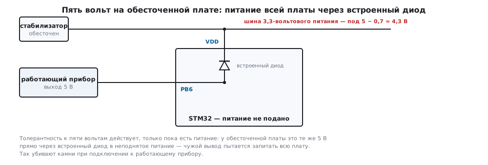
⚠️ Five-volt tolerance works only while the supply is present. The limit of a tolerant pin is the supply plus 4 V: without power that is 4 V, and five volts on the input of an unpowered board exceed it. This is how chips are killed when connected to a running instrument. On regular pins the same thing happens through the built-in diode, which tries to power the chip from the input.
62.2 Injected current: the key number of this section
When the voltage on a pin goes above the supply, the built-in diode opens and clamps the input at 4.0 V (supply plus the diode drop). The current is then limited only by the external circuit — and the allowed current is tiny:
| Current | |
|---|---|
| per pin | 5 mA |
| total for the package | 25 mA |
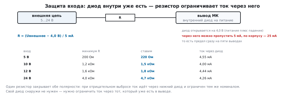
So the maximum injected current can be allowed at the same time on only five pins. All the practice of input protection follows from this: the diode inside is already there, you do not need to add your own — you need to limit the current through the one that exists. A series resistor does this.
Two caveats about these 5 mA — they are in the absolute maximum ratings table, not in the
operating one. A negative injected current (input below ground) on F103, according to the description,
noticeably degrades conversion on other ADC channels, and on analog
inputs where it is possible, a Schottky diode to ground is recommended;
a positive one within the limit does not disturb ADC accuracy. And the positive current
flows through the diode into the VDD rail: if the board draws less at that moment
(sleep, microamperes), the linear regulator cannot absorb the incoming current,
and VDD creeps up. That is why a continuous current through the diode is designed for
fractions of a milliampere (62.3).
62.3 Series resistor: calculation
The resistor is calculated from the excess over the clamping level:
R = (Uвнешнее − 4,0 В) / 5 мА
| Input | Minimum | We fit | Actual current |
|---|---|---|---|
| 5 V | 200 Ω | 220 Ω | |
| 10 V | 1.2 kΩ | 1.5 kΩ | 4.0 mA |
| 12 V | 1.6 kΩ | 1.8 kΩ | |
| 24 V | 4.0 kΩ | 4.7 kΩ | 4.26 mA |
Here Uвнешнее is the external voltage. One resistor covers both polarities: on a negative spike the current
flows through the lower diode and is limited by the same value.
This value is the minimum against an accidental spike. If the external voltage
sits on the input permanently — a 24 V signal applied for hours — all that current
flows through the diode into VDD all the time (62.2). Then the resistor is calculated for fractions
of a milliampere: for 24 V, 47 kΩ gives 0.43 mA, 100 kΩ gives 0.20 mA, and the input
becomes logic-only and slow (62.7). For a permanent
overvoltage a divider is more convenient (62.4): it keeps the input below the supply, and the diode
does not open at all.
⚠️ The calculation is valid only for regular pins. A pin that is tolerant to 5 V has no diode to
VDD— that is why it can take 5 V — and a positive injected current is not allowed at all in the F103 description: −5/+0 mA. The resistor limits nothing here, and 12 V will reach the pin in full — far beyond itsVDD+ 4 V limit. A voltage above 5 V is applied to such a pin only through a divider (62.4) or with an external clamp after the resistor — a Zener diode or a Schottky diode to 3.3 V.
This is the cheapest protection there is, and it covers most everyday cases: a swapped wire, pickup from a power line, someone else's logic level.
62.4 A divider, when the voltage must also be measured
A resistor limits the current, but the input is still clamped at 4 V — you cannot measure with it. For measurement a divider is used (section 50.2).
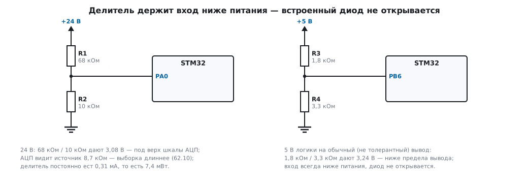
For 24 V, 68 kΩ / 10 kΩ fits: the output is 3.08 V — right at the top of the ADC scale, without exceeding it. But a divider is calculated for the upper limit: if industrial "24 V" goes up to 30 V, 68/10 gives 3.85 V from it — above the scale. Then you take 82 kΩ / 10 kΩ: from 30 V — 3.26 V, from 24 V — 2.61 V, source resistance for the ADC — 8.9 kΩ.
We pay for this twice:
- the resistance the ADC sees becomes 8.7 kΩ — this lengthens the sampling (section 14.2);
- the divider constantly draws 0.31 mA, that is 7.4 mW. On mains power that is nothing, on battery power it is a noticeable part of the budget.
For a five-volt logic signal to a regular (not tolerant) pin a divider of 1.8 kΩ / 3.3 kΩ is enough: it gives 3.24 V, below the limit of a regular pin.
62.5 The reverse task: 3.3 V into a five-volt input
There is a trap here, because going "down" is simple, and going "up" is not.
| What receives the signal | Logic one threshold | Will it accept 3.3 V? |
|---|---|---|
| five-volt CMOS logic | 3.5 V | no: the guaranteed 2.9 V (59.5) is 0.6 V short, even 3.3 V without load is 0.2 V short |
| logic with TTL inputs | 2.0 V | yes, 0.9 V margin at the guaranteed level, 1.3 V without load |
Even 0.2 V short is exactly the case where "it works on the bench but not in the product": the threshold drifts with temperature and from part to part.
Options: use a receiver with TTL inputs, add a level shifter, or use an open-drain pin with a pull-up to five volts — if the pin is tolerant.
62.6 Output current budget
There is a limit not only on the input. On F103:
| Current | |
|---|---|
| one pin | 25 mA |
| through the supply pins — together with the chip's own consumption | 150 mA |
| the chip itself at 72 MHz with all peripherals | up to 50 mA |
The total limit is stricter than the per-pin one: 100 mA is left for the pins, and the maximum current can be drawn from only four pins. The classic example is eight LEDs at 20 mA each: that is 160 mA — more than the whole limit even without the chip itself, and 60 % more than what is left for the pins. They will light, the chip will most likely survive, but the rating is violated, and in hot weather this will show.
Other families have their own numbers: F4 has the same 25 mA per pin, but 240 mA through the supply; G4 has 20 mA per pin and 100 mA for all pins (section 49.7).
The right solutions: reduce the current to 5–7 mA (modern LEDs are bright enough at that), add a driver, or switch to a multiplexed display (section 57.4).
62.7 RC filter at the input
The protection resistor and a capacitor also give you a filter. The classic 10 kΩ and 100 nF:
| Value | |
|---|---|
| time constant | 1 ms |
| cutoff frequency | 159 Hz |
| time to the logic one threshold | 1.2 ms |
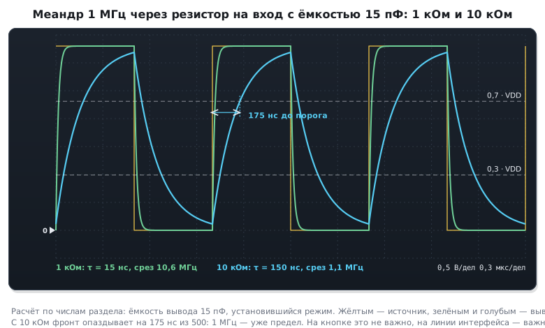
Such a filter smooths out the bounce of a mechanical contact. But note the price: the input has become slow, and you have to account for it.
| Resistor | Line speed limit (pin capacitance 15 pF) |
|---|---|
| 1 kΩ | 10.6 MHz |
| 10 kΩ | 1.1 MHz |
Ten kilohms on an interface line is already a ceiling of a megahertz. That is why a button gets 10 kΩ, and a signal line gets 100…330 Ω.
62.8 ESD: why the built-in protection is not enough
A chip is tested for discharge using the human body model, and the datasheet gives the corresponding figure. In the field a different discharge arrives.
| Human body model, 2 kV | Contact discharge, 8 kV | |
|---|---|---|
| capacitance / resistance | 100 pF / 1500 Ω | 150 pF / 330 Ω |
| peak current | 1.33 A | 24.2 A |
| energy | 200 µJ | 4.8 mJ |
The difference: 24 times in energy and 18 times in current. The built-in protection is not designed for this and does not have to be — it protects the die during assembly, not the product in use.
The conclusion is simple: everything that leaves the enclosure is protected separately — connectors, panel buttons, sensor wires. Internal lines between chips on the same board do not need it.
62.9 External suppressor: what you pay
The stand-off voltage of a suppressor is the voltage up to which its low leakage is specified. It is chosen no lower than the highest voltage on the line: for a 3.3 V line — a part for 3.3–3.6 V or for 5 V, for a 5 V line — for 5 V and above. Lower is not allowed: the part will start to leak at the working voltage and distort the signal, and at an ADC input — distort the readings; higher is allowed, but then it also clamps later.
And most importantly: during a discharge the suppressor holds its clamping voltage at the pulse current — it is higher than the breakdown voltage (173.3), and the breakdown is higher than the stand-off. The suppressor from the model in 173.3 has a dynamic resistance of 0.35 Ω, and the 24.2 A contact discharge peak (62.8) adds 0.35 · 24.2 ≈ 8.5 V to the breakdown — many times more than the pin can take (62.1). That is why the suppressor is placed at the connector, followed by a resistor of tens or hundreds of ohms, and only then the pin: the remaining current, already limited by the resistor, is taken by the built-in diode.
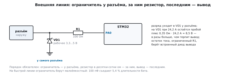
The second characteristic is capacitance, and on fast lines it decides everything. With a bit length of 83.3 ns (12 Mbit/s) and a line impedance of 45 Ω:
| Suppressor capacitance | Share of the bit length it eats |
|---|---|
| 3 pF | 0.16 % |
| 100 pF | 5.4 % |
Five percent of the edge is already visible by eye, let alone on an instrument. A high-power suppressor goes on the supply and on slow lines, and on interface lines — a dedicated low-capacitance one.
Where the interference arrives not as a discharge but over a communication line with a large ground potential difference, a resistor and a suppressor will not help at all — you need galvanic isolation (section 54).
62.10 Protection versus measurement
A protection resistor on an analog input adds to the source resistance and lengthens the ADC sampling (section 14.2):
| Resistor | Required sampling time |
|---|---|
| 1 kΩ | 42 ns |
| 10 kΩ | 416 ns |
| 100 kΩ | 4.2 µs |
The divider from 62.4 gives 363 ns — acceptable. But 100 kΩ on a fast measurement is no longer acceptable: either set a long sampling time, or add a buffer after the protection (section 56.1) — it both isolates and lets you keep the resistor large.
62.11 Unused pins
| How to leave it | What you get |
|---|---|
| analog input | no current flows, the input is disconnected from the logic — this is the right way |
| output driven low | also acceptable, but an assembly error will short it |
| input with pull-up | works; almost no current flows — the pin already sits at the pull-up level (82 µA only if the pin is held at the opposite level) |
| input without pull-up | floats, picks up noise, heats the input stage |
Analog mode is still better: it disconnects the input Schmitt trigger, and the pin does not react to noise. A pull-up is expensive only if the pin on the board is connected to something that holds the opposite level: then it is 3.3 V / 40 kΩ = 82 µA per pin, and twenty such pins on battery power already cost hours of operation.
A floating input is not only about consumption. The input stage in an undefined state switches from noise, and this looks like random failures that "cannot be reproduced".
62.12 Pitfalls
The chip died after being connected to an instrument. Five volts arrived at an unpowered board: tolerance works only while the supply is present.
The input reads 4 V instead of 10. That is how it should be: the built-in diode clamped it. For measurement you need a divider, not a resistor.
The board works, but a pin has "weakened". The injected current was exceeded; the die has degraded, and the pin must be considered lost.
Communication with a five-volt chip works every other time. Its logic one threshold is 3.5 V, and the output gives 3.3.
Eight LEDs heat up the chip. The total budget is exceeded: on F103 no more than 150 mA goes through the supply, and that includes the chip's own consumption.
A button with a 10 kΩ + 100 nF filter "does not press". Polling happens faster than the input reaches the threshold — the filter needs 1.2 ms.
The interface does not work after protection was added. A 10 kΩ resistor limited the line to a megahertz; signal lines get hundreds of ohms.
The USB edge got worse after a suppressor was added. Capacitance: you need a low-capacitance one.
The ADC "lags" after protection was added. The resistor lengthened the sampling; add a buffer or increase the sampling time.
Random failures on the board for no reason. Unused pins are left floating.
The device breaks from static while the board is powered. The external lines are protected only by the built-in structures — they are not designed for this.
62.13 Summary
- The operating range of a pin is from −0.3 V to the supply plus 0.3 V; a tolerant one takes 5.5 V, but only while the supply is present.
- The injected current is 5 mA per pin and 25 mA in total; protection comes down to limiting the current through the diode that is already there.
- The resistor is calculated as the excess over 4.0 V divided by 5 mA: 1.5 kΩ
for 10 V, 4.7 kΩ for 24 V — only for regular pins: a tolerant one
has no diode to
VDD, and a positive injected current is not allowed. - Measurement needs a divider: 68 k / 10 k gives exactly 3.08 V from 24 V at the cost of 8.7 kΩ of source resistance and 7.4 mW of consumption.
- A signal does not go up in level: five-volt CMOS logic is 0.2 V short, TTL inputs accept it with a 1.3 V margin.
- The total budget is stricter than the 25 mA per pin: on F103, 150 mA goes through the supply including the chip, about 100 is left for the pins, and eight LEDs at 20 mA exceed this by 60 %.
- A 10 kΩ and 100 nF filter gives 1.2 ms to the threshold and limits the line to 1.1 MHz — not acceptable on signal lines.
- A contact discharge carries 24 times more energy than the model the die was tested with: external lines are protected separately, and the suppressor is chosen by stand-off voltage, clamping voltage and capacitance, with a resistor placed between it and the pin.
- Unused pins are set to analog input.
Next: Part IX, section 63 "How text becomes a program; number systems" — from electronics to the language in which all of this is described.