 Embedded HandbookApps
61. Minimal circuit around the microcontroller: start-up conditions
A microcontroller is not a chip you can simply solder down and power up. It has start-up conditions, and if even one of them is not met, the board behaves unpredictably: sometimes it starts, sometimes not, sometimes it works for a week and then resets.
This section covers what must be on the board, what is desirable, what you can leave out — and what happens if you save on each item.
Terms used in the documentation
Term Meaning power-on reset (POR) reset held while power comes up brown-out reset (BOR) reset when the supply sags reset temporization delay after the threshold is reached VDD rise / fall time rate how fast the supply rises and falls NRST the reset pin internal pull-up (RPU) the built-in pull-up resistor filtered / not filtered pulse a pulse that is rejected / one that is guaranteed to pass decoupling capacitors that keep the supply clean VDDA, VREF+ supply and reference of the analog part load capacitance (CL) the capacitance a crystal expects to see stray capacitance parasitic capacitance of traces and pins boot mode where the chip starts from
61.1 Power: every pin, and a capacitor on each
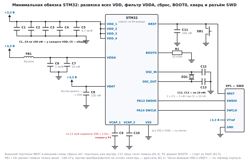
In a 48–64 pin package the supply goes to four pairs of pins. You must connect all of them — not "at least one". Inside the die they power different regions, and an unconnected pair means that part of the circuit is powered through parasitic paths.
Each pin gets a 100 nF capacitor, physically right next to it (section 53.5), plus one common 4.7 µF capacitor.
Besides VDD and VSS there are pins that are easy to miss. On F4 these are VCAP_1 and VCAP_2 — the output of the internal core regulator: each needs a 2.2 µF ceramic capacitor with ESR below 2 Ω to ground; without them the core will not start or will misbehave. VBAT goes to a battery or, if there is none, to VDD with 100 nF. VREF+, where it has its own pin (on F407 — in packages from 100 pins), goes to VDDA or to a voltage reference. The number and purpose of the supply pins come from the pinout table of the specific package.
The analog supply is brought in separately and filtered: a ferrite bead and capacitors of 1 µF and 10 nF. A bead is not an inductor of hundreds of microhenries: its "600 Ω" is specified at 100 MHz, and at low frequencies it behaves like an inductance of about 1 µH (section 168.3). With 1 µF this is a filter with a cutoff of about 160 kHz: it attenuates noise at 500 kHz only about nine times, and near the cutoff a resonant peak is possible. A bead mostly suppresses noise at tens of megahertz; against the ripple of a switching converter at hundreds of kilohertz you need a real inductor of tens of microhenries or a separate linear regulator between the input and the converter (section 55.6). Without this the ADC will measure the noise of its own power supply.
61.2 Start-up thresholds
The numbers in this subsection are for G4; F103 and F407 have a different reset circuit, and their table is at the end of the subsection. The chip is held in reset until the supply has risen to the threshold. The lowest level is always on:
| Voltage | |
|---|---|
| start-up threshold (typical) | 1.66 V |
| spread between parts | 1.62 … 1.70 V |
| hysteresis | 20 mV |
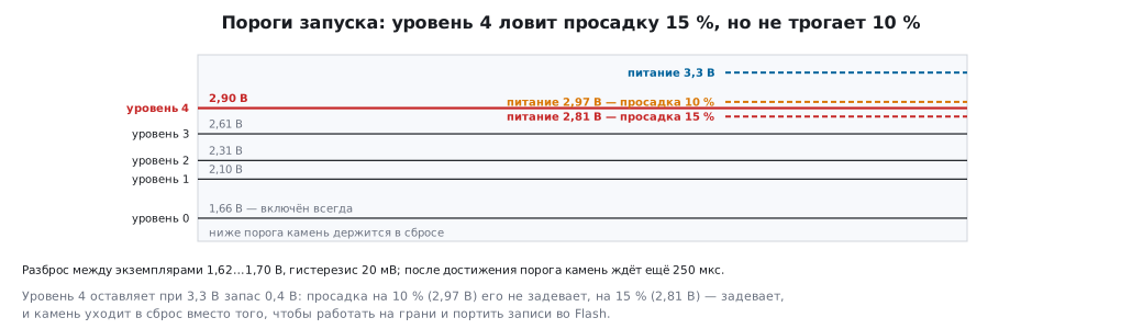
In addition you can enable one of the configurable levels:
| Level | Threshold |
|---|---|
| 0 (always) | 1.66 V |
| 1 | 2.10 V |
| 2 | 2.31 V |
| 3 | 2.61 V |
| 4 | 2.90 V |
Why you need them: with a 3.3 V supply, level 4 leaves a 0.4 V margin. A sag of 10 % does not reach it yet (2.97 versus 2.90), but a sag of 15 % does — and the chip goes into reset instead of running on the edge and corrupting data in Flash. For devices that store settings this matters more than it seems.
After the threshold is reached the chip waits another 250 µs (up to 400 in the worst case) before it starts executing the program. During this time the internal oscillator starts and the configuration bytes are loaded.
F103 and F407 have fewer levels, and they are set differently:
| F103 | F407 | |
|---|---|---|
| start-up threshold (typical) | 1.92 V | 1.72 V |
| brown-out reset | not configurable | three levels in the configuration bytes: 2.19 / 2.50 / 2.83 V; off from the factory |
| delay after the threshold | 2.5 ms (1…4.5) | 1.5 ms (0.5…3) |
| PVD detector, 8 levels | 2.08…2.78 V | 2.04…3.03 V |
The brown-out and detector levels are given for a falling supply. The detector (section 10.7) only raises an interrupt: on F103 the program must go into reset on a sag by itself.
61.3 Supply rise and fall rate
There are two asymmetric requirements here, and the second is often overlooked.
The rise is not specified at all — from zero to infinity. The chip starts at any supply rise rate, whether instantaneous or over seconds.
The fall is limited from below: no faster than 10 µs per volt, that is, from 3.3 V to zero — no faster than 33 µs. The reset circuit cannot track a drop that is too sharp, and the chip may start executing the program with insufficient supply.
In practice the requirement is met by itself: a 10 µF capacitor on the supply at a 50 mA load discharges in 660 µs — twenty times slower than the limit. But if the supply is switched off by a switch with a fast fall and no capacitor, it is worth checking.
61.4 The reset pin
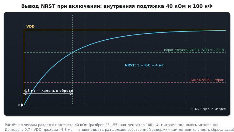
There is already a 25…55 kΩ pull-up inside, typically 40. An external pull-up resistor is not needed — it is the most common unnecessary part on hobby boards.
The reset button is connected straight to ground: up to 132 µA flows through the internal pull-up, and no series resistor is needed. For the reset to work, the pin must be below 0.99 V (with a 3.3 V supply).
The input filter rejects short glitches:
| Pulse length | What happens |
|---|---|
| shorter than 70 ns | guaranteed to be filtered out |
| 70…350 ns | a matter of luck |
| longer than 350 ns | guaranteed to pass |
A 100 nF capacitor on the reset pin is needed — not to shape the reset, but to protect against noise. With the 40 kΩ pull-up it gives a time constant of 4 ms, and it takes 4.8 ms to reach the release threshold — that is twelve times longer than the chip's own delay. So with this capacitor the reset length is set by the capacitor.
⚠️ No special reset circuit is needed. Inside there is a power-on reset, a brown-out reset, a filter and a pull-up. An external supply supervisor is used only where the requirements are stricter than the built-in ones — and then it is chosen deliberately, not "just in case".
61.5 Boot mode selection
The boot selection pin (or pins) determines where the chip starts from: Flash, system memory with the factory bootloader, or RAM (section 4.7).
It must not be left floating: a pin pulled to nothing picks up noise, and the chip starts sometimes from its own program, sometimes from the bootloader — "every other time", and differently depending on whether you are holding the board in your hands.
The right way: a 10 kΩ resistor to ground (or to the supply if you want the bootloader by default) and, if useful, a jumper or a button.
61.6 Crystal: when it is needed and how to calculate
The internal oscillator is enough for most tasks: its error is about 1 %, which is enough for UART up to 115200 and for any logic. A crystal is needed when:
- USB runs on F1 or F4 — it needs accuracy better than 0.25 % (section 20).
G4, like F072 (section 6), has an internal 48 MHz oscillator
(
HSI48) that is trimmed by frames from the host (theCRSblock), and a USB device works without a crystal; - you need a real-time clock — then a 32768 Hz watch crystal;
- time or frequency is measured;
- communication runs at high speed or over a long line.
The capacitors are calculated from the crystal's load capacitance, not taken as "22 pF like everyone else":
C = 2 × (CL − Cмонтажа)
Here Cмонтажа is the stray capacitance of traces and pins — about 5 pF. For a crystal with
a load capacitance of 10 pF you need 10 pF capacitors, for 20 pF — 30 pF each.
If the stray capacitance turns out to be more than half the load capacitance, external
capacitors are not needed at all.
The cost of a mistake for a watch crystal: 5 pF off is about 75 ppm, that is 6.5 seconds per day and 39 minutes per year. A clock that "drifts" is almost never a "bad crystal" but wrong capacitors.
Traces to the crystal are short, with ground around them, and nothing fast nearby.
61.7 Debug connector
Four signals: two data lines, ground and power. It is useful to bring out reset as the fifth — it lets the debugger catch a chip that manages to go to sleep or reassign the debug pins (section 4.4).
Put the connector even on a board where debugging is "not planned": pads for pogo pins take up millimetres, and without them reflashing requires desoldering.
61.8 Summary: mandatory and desirable
| What | Needed |
|---|---|
| all supply pins connected | mandatory |
| 100 nF at each supply pin | mandatory |
| common 4.7 µF capacitor | mandatory |
| filtered analog supply | mandatory, even if the ADC is not used |
| boot selection pin tied with a resistor | mandatory |
| 100 nF capacitor on the reset pin | strongly recommended |
| debug connector or pads | strongly recommended |
| reset button | desirable |
| crystal | depends on the task |
| external reset pull-up resistor | not needed |
| external reset circuit | not needed |
61.9 Pitfalls
The board does not start. Check in order: power on all pins, the boot selection pin, the reset pin is not held to ground, the analog supply.
It starts every other time. The boot selection pin is floating.
It works until you touch the board. The same thing — the capacitance of your hand changes the noise picked up by the floating pin.
The debugger does not see the chip. The program has reassigned the debug pins or gone to sleep; connect reset to the debugger and use the "connect under reset" mode.
The ADC returns garbage. There is no analog supply, or it is not filtered.
Random resets. No capacitor on the reset pin, or a supply sag reaches the threshold.
The clock drifts by minutes per year. The crystal capacitors do not match its load capacitance.
The crystal does not start. Capacitors too large, long traces, a crystal for the wrong load capacitance.
An external reset circuit was added and things got worse. It conflicts with the built-in one and prevents the debugger from toggling reset.
61.10 Summary
- All supply pins are connected, each has 100 nF right next to it, plus a common 4.7 µF and a separate filter on the analog supply. A bead with 1 µF only cuts from ~160 kHz; against converter noise — an inductor.
- On F4 — 2.2 µF of ceramic on each of VCAP_1 and VCAP_2; VBAT without a battery — to VDD with 100 nF.
- G4 starts at 1.66 V and then waits 250 µs (up to 400); F103 — at 1.92 V and 2.5 ms, F407 — at 1.72 V and 1.5 ms.
- The configurable G4 threshold of 2.90 V with a 3.3 V supply catches a 15 % sag without reacting to a 10 % sag; on F407 the 2.83 V level does the same, F103 has no configurable threshold.
- The supply rise is not specified; the fall must be no faster than 10 µs per volt, and a 10 µF capacitor meets this with a twentyfold margin.
- The reset pin already has a 25…55 kΩ pull-up: an external resistor and an external reset circuit are not needed. A 100 nF capacitor gives 4.8 ms of reset.
- The boot selection pin must not be left floating — that is where "starts every other time" comes from.
- Crystal capacitors are calculated with the formula
2 × (CL − Cstray); a 5 pF mistake for a watch crystal means 39 minutes per year.
Next: section 62 "Pin protection" — what happens when something the board did not expect arrives from outside.