 Embedded HandbookApps
130б. Heat on the board: thermal resistance, copper area and vias under the package
In section 55.4 the die temperature of a regulator was calculated in one line:
Tj = Tamb + P × Rth, and for SOT-223 we took 60 °C/W. Section 204.4 does
the same for the microcontroller, with θJA from the STM32 datasheets. But where does
this number come from, and why can the same package have 60 one time and 150 another? The
junction-to-air thermal resistance is a property not of the package but of the package
together with the board: how much copper is under it, how thick it is, whether there is a bottom
layer and what connects it to the top one.
Here this is calculated. A board model of our own on the computer — a grid of cells 0.25 mm across, copper and glass-epoxy laminate, vias, heat transfer to the air — answers practical questions: how many square millimetres of copper a regulator dissipating 0.5–1.5 W needs, how many vias to place and when they are useless. Then the same model calculates the power section of the board from section 131 in four variants, built by a KiCad script and checked by DRC, and compares the results with the θJA tables from the F103 and F407 datasheets.
Sources: the STM32F103x8/B datasheet (DocID13587 Rev 17, section 6.9, Table 62;
the UFQFPN48 and VFQFPN36 packages — Tables 52 and 51) and STM32F405/407 (DS8626 Rev 9, section 6.7,
Table 98). The idea comes from TI application note SNVA419 on thermal calculation with
a "resistor" chain; its text and graphs are not used in this section.
The model and all listings are our own: heat130b.py (the model), study130b.py
(the experiments), kicad130b.py (the board in KiCad), ref130b.py (an independent
cross-check).
Terms used in the documentation
Term Meaning thermal resistance junction-ambient, ΘJA thermal resistance from the die to the surroundings junction-to-case, ΘJC die to package (for SOT-223 — die to tab) junction temperature, TJ temperature of the die power dissipation, PD power turned into heat natural convection (still air) natural convection, air that does not move exposed pad (exposed die pad) bare metal pad under the package thermal via a via placed to carry heat away copper pour, copper area a copper fill zone, the copper area thermal relief thin spokes between a pad and a copper zone heat spreading heat flowing sideways through copper plating thickness thickness of the copper plating in a hole 1s / 2s2p test board test board: one layer / two signal and two solid planes
130б.1 θJA is a property of the board, not of the package
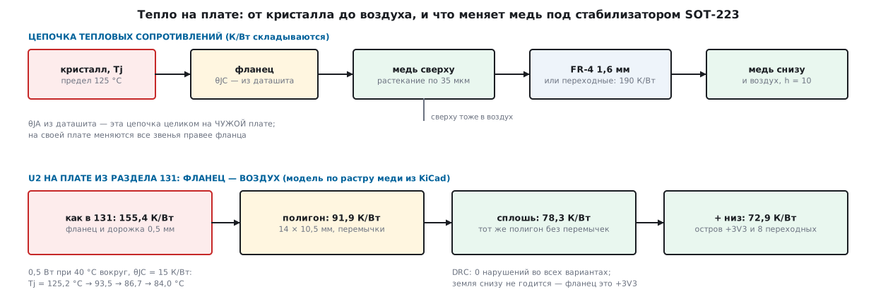
Heat leaves the die along a chain: die — tab or leads — board copper — through the laminate or through vias to the other layer — into the air on both sides. Each link is a thermal resistance in K/W (the same as °C/W), and the links add up in series, like resistors. The die temperature rise above the air is the power multiplied by the sum.
The inner link — "junction to case", θJC — is set by the manufacturer, and
it is small. Everything else is the board. So the θJA from a datasheet is the whole chain
on the manufacturer's board. The STM32 datasheets do not say what that board is:
both only state that the conditions are JESD51-2, natural
convection in still air, and give the formula TJ max = TA max + (PD max × ΘJA).
The tables themselves show that the board is what matters. For the F103, the LQFP48 and UFQFPN48 packages are both 7 × 7 mm with a 0.5 mm pitch, yet θJA is 55 and 32 °C/W. They differ in one thing: UFQFPN48 has an exposed pad of 5.6 × 5.6 mm underneath (D2 = E2 = 5.600 typical), soldered to the board. The datasheet recommends connecting it to VSS (note 2 to figure 44). Yet VFQFPN36 has a smaller pad — 3.7 mm — and its θJA is only 18 °C/W: you cannot compare packages from one table unless you know what boards they were measured on.
| Package | θJA, F103 | θJA, F407 |
|---|---|---|
| LQFP48 7 × 7 mm | 55 °C/W | — |
| UFQFPN48 7 × 7 mm, exposed pad | 32 °C/W | — |
| VFQFPN36 6 × 6 mm, exposed pad | 18 °C/W | — |
| LQFP64 10 × 10 mm | 45 °C/W | 46 °C/W |
| LQFP100 14 × 14 mm | 46 °C/W | 43 °C/W |
| LQFP144 20 × 20 mm | — | 40 °C/W |
What to do about this on your own board is shown by the model: it calculates the links to the right of the tab — "pad to air" — for any copper.
130б.2 The model: a grid of cells, copper and laminate
The board is divided into square cells 0.25 mm on a side. Each copper layer is its own sheet of nodes. Within a layer, neighbouring nodes are connected by the conductance of copper, if the cell has copper, plus their share of the laminate along the board. Layers are connected to each other by the conductance of FR-4 across the board and by the walls of the vias. Heat leaves the top and bottom surfaces into the air. The board edges are thermally insulated. The source is 1 W of power, split equally over the cells of the component's pad. The "pad to air" thermal resistance is the average temperature rise of those cells.
The material properties are assumed, not measured:
| Quantity | Assumed |
|---|---|
| thermal conductivity of copper | 390 W/(m·K) |
| FR-4 across the board | 0.30 W/(m·K) |
| FR-4 along the board | 0.80 W/(m·K) |
| heat transfer to air on each side (convection and radiation) | h = 10 W/(m²·K) |
| copper on the hole wall | 25 µm |
| board thickness | 1.6 mm |
The result is a system of linear equations "conductances × temperatures =
powers". The matrix is symmetric and positive definite, so it is solved
by the conjugate gradient method. The matrix itself is not stored: the apply function
computes the heat flows with numpy array slices. The whole model:
# -*- coding: utf-8 -*-
"""Раздел 130б: тепловая модель печатной платы методом конечных разностей.

Плата — сетка квадратных ячеек со стороной d. Каждый слой меди — свой лист узлов; медь есть там,
где маска слоя True. Между соседними узлами слоя тепло течёт по меди и по стеклотекстолиту FR-4,
между слоями — поперёк FR-4 и по стенкам переходных отверстий. С верхней и нижней поверхности
тепло уходит в воздух с коэффициентом h. Источник — мощность P, равномерно на площадке детали.
Нужен только numpy."""
import math
import numpy as np

K_CU = 390.0      # Вт/(м·К), теплопроводность меди (принято)
K_FR4_Z = 0.30    # Вт/(м·К), FR-4 поперёк платы (принято)
K_FR4_XY = 0.80   # Вт/(м·К), FR-4 вдоль платы (принято)
H_AIR = 10.0      # Вт/(м²·К) с каждой стороны: конвекция и излучение в неподвижном воздухе (принято)
T_PLATE = 25e-6   # м, медь на стенке переходного отверстия (принято)


def via_r(drill, plating=T_PLATE, length=1.6e-3):
    """Тепловое сопротивление одного переходного отверстия, К/Вт: медная трубка
    с внутренним диаметром drill и стенкой plating, длиной length; середина пустая."""
    r_out = drill / 2
    r_in = r_out - plating
    area = math.pi * (r_out ** 2 - r_in ** 2)
    return length / (K_CU * area)


def sheet(t_cu, mask, fr4_share):
    """Проводимость слоя «на квадрат», Вт/К: медь там, где маска, плюс доля FR-4 вдоль платы."""
    return K_CU * t_cu * mask + K_FR4_XY * fr4_share


def pair(s1, s2):
    """Проводимость между центрами двух соседних квадратных ячеек: две половинки последовательно."""
    return 2 * s1 * s2 / (s1 + s2)


def build(d, masks, t_cu, gaps, vias, h=H_AIR, drill=0.3e-3):
    """Проводимости сетки. masks — список масок слоёв (ny, nx) сверху вниз, t_cu — толщины меди, м,
    gaps — толщины FR-4 между соседними слоями, м, vias — число переходных в каждой ячейке (ny, nx),
    drill — диаметр отверстия, м.
    Возвращает словарь: gx, gy — вдоль слоёв, gz — между слоями, gh — в воздух."""
    L = len(masks)
    share = [((gaps[l - 1] if l > 0 else 0) + (gaps[l] if l < L - 1 else 0)) / 2 for l in range(L)]
    S = np.array([sheet(t_cu[l], masks[l].astype(float), share[l]) for l in range(L)])
    gx = pair(S[:, :, :-1], S[:, :, 1:])
    gy = pair(S[:, :-1, :], S[:, 1:, :])
    via_g = 1.0 / via_r(drill, length=1.0)             # проводимость стенки отверстия на метр длины, Вт·м/К
    gz = np.array([np.broadcast_to(K_FR4_Z * d * d / g + vias * via_g / g, S[0].shape) for g in gaps])
    gh = np.zeros_like(S)
    gh[0] = h * d * d
    gh[-1] = h * d * d
    return {"gx": gx, "gy": gy, "gz": gz, "gh": gh}


def apply(G, T):
    """Поток тепла из каждого узла при температурах T (перегрев над воздухом), Вт: A·T."""
    q = G["gh"] * T
    f = G["gx"] * (T[:, :, :-1] - T[:, :, 1:])
    q[:, :, :-1] += f
    q[:, :, 1:] -= f
    f = G["gy"] * (T[:, :-1, :] - T[:, 1:, :])
    q[:, :-1, :] += f
    q[:, 1:, :] -= f
    f = G["gz"] * (T[:-1] - T[1:])
    q[:-1] += f
    q[1:] -= f
    return q


def diag(G):
    """Диагональ матрицы A: сумма проводимостей, сходящихся в узле."""
    a = G["gh"].copy()
    a[:, :, :-1] += G["gx"]
    a[:, :, 1:] += G["gx"]
    a[:, :-1, :] += G["gy"]
    a[:, 1:, :] += G["gy"]
    a[:-1] += G["gz"]
    a[1:] += G["gz"]
    return a


def solve(G, q, tol=1e-9, maxit=50000):
    """Сопряжённые градиенты с диагональным предобусловливанием: A·T = q. Возвращает T и число шагов."""
    D = diag(G)
    T = np.zeros_like(q)
    r = q.copy()
    z = r / D
    p = z.copy()
    rz = np.sum(r * z)
    nb = math.sqrt(np.sum(q * q))
    for it in range(1, maxit + 1):
        Ap = apply(G, p)
        a = rz / np.sum(p * Ap)
        T += a * p
        r -= a * Ap
        if math.sqrt(np.sum(r * r)) < tol * nb:
            return T, it
        z = r / D
        rz_new = np.sum(r * z)
        p = z + (rz_new / rz) * p
        rz = rz_new
    raise RuntimeError("CG не сошёлся")


def theta(d, masks, t_cu, gaps, vias, src, P=1.0, h=H_AIR):
    """Тепловое сопротивление площадка–воздух, К/Вт: средний перегрев ячеек источника на ватт.
    src — маска ячеек верхнего слоя, куда входит мощность P. Возвращает (θ, баланс, шаги)."""
    G = build(d, masks, t_cu, gaps, vias, h)
    q = np.zeros((len(masks),) + src.shape)
    q[0][src] = P / src.sum()
    T, it = solve(G, q)
    out = float(np.sum(G["gh"] * T))                   # что ушло в воздух — должно быть P
    return float(T[0][src].mean()) / P, out / P, it


def rect(ny, nx, d, x0, y0, x1, y1):
    """Маска прямоугольника [x0, x1) × [y0, y1) в метрах по центрам ячеек."""
    yc = (np.arange(ny) + 0.5) * d
    xc = (np.arange(nx) + 0.5) * d
    return ((yc[:, None] >= y0) & (yc[:, None] < y1)) & ((xc[None, :] >= x0) & (xc[None, :] < x1))
It is checked in two ways (ref130b.py, numpy 2.3.3 and scipy 1.18.1).
The first is an exact solution. If the copper in each layer is solid, the temperature
can be expanded in a cosine series along the board, and each harmonic
leaves a 2 × 2 system. The grid converges to the series: on a 50 × 50 mm board
with 35 µm copper on both sides the difference is 0.74 % with a 0.5 mm step, 0.19 %
with 0.25 mm and 0.05 % with 0.125 mm. The second is the same board from section 131,
but with the matrix built again edge by edge with scipy.sparse and solved by the direct
method spsolve: all four variants from 130б.6 agreed with the conjugate
gradients to the third digit. Every calculation also checks the balance:
everything put in leaves into the air to within 10⁻⁶.
def exact(L, src, s1, s2, M=1500):
    """Средний перегрев прямоугольника src = (x0, y0, x1, y1) на ватт: ряд по cos(mπx/L)cos(nπy/L)."""
    x0, y0, x1, y1 = src
    m = np.arange(M)
    km = m * math.pi / L

    def integ(a, b):
        out = np.empty(M)
        out[0] = b - a
        out[1:] = (np.sin(km[1:] * b) - np.sin(km[1:] * a)) / km[1:]
        return out

    ix, iy = integ(x0, x1), integ(y0, y1)
    eps = np.where(m == 0, 1.0, 2.0)
    area = (x1 - x0) * (y1 - y0)
    q = (eps[:, None] * eps[None, :]) * np.outer(iy, ix) / (L * L) / area     # P = 1 Вт
    k2 = km[:, None] ** 2 + km[None, :] ** 2
    g = KZ / TB
    a11, a22 = s1 * k2 + H + g, s2 * k2 + H + g
    t1 = q * a22 / (a11 * a22 - g * g)
    return float(np.sum(t1 * np.outer(iy, ix)) / area)
Of the assumed numbers, h shifts the result the most. Still air is not a number from a handbook but a range, and the model does not refine it: with h = 7, 10 and 14 W/(m²·K), a regulator with 20 × 20 mm of copper on both sides gets 69.3, 57.6 and 48.7 K/W. So the model's numbers are for comparing variants with each other, and the temperature margin should be no less than 20 %.
130б.3 A via and a copper layer
A via is a copper tube: it is empty inside (or filled with solder mask),
and heat flows only through the wall. Its cross-section is a ring, and the resistance
of one via through the 1.6 mm board thickness takes one line to calculate
(via_r in the listing above):
| Hole | Wall 18 µm | 25 µm | 35 µm |
|---|---|---|---|
| 0.2 mm | 399 K/W | 298 K/W | 226 K/W |
| 0.3 mm | 257 K/W | 190 K/W | 141 K/W |
| 0.4 mm | 190 K/W | 139 K/W | 102 K/W |
One via is hundreds of K/W: on its own it is a poor heat path. But compare it with what would be there instead: 1.6 mm of laminate under a 1 × 1 mm square is 5333 K/W. One 0.3 mm via (as in the default KiCad rules from section 130.6) conducts as much as 28 such squares. Eight vias under the tab give 24 K/W in parallel, against hundreds through FR-4 under the same pad.
A copper layer is described "per square", like the resistance of a film: the conductance of a
square does not depend on its size. For 35 µm copper it is 0.0136 W/K —
10.7 times more than the whole 1.6 mm thickness of FR-4 along the board; for 70 µm it is
0.0273 W/K, 21.3 times more. The same gives the distance heat manages to
spread before it leaves into the air, √(S / 2h): about 27 mm for 35 µm
and 37 mm for 70 µm. Copper farther than this from the source does almost
no work — you can see this in the next table.
130б.4 Copper area and vias under SOT-223
The experiment: a regulator in SOT-223 in the middle of a 50 × 50 mm double-sided board.
Heat enters through a 2.0 × 3.8 mm tab (the pad size is from the
KiCad footprint SOT-223-3_TabPin2; on the 0.25 mm grid it
becomes 2.0 × 4.0 mm). Around the tab is a square of copper with side a.
Four variants: copper on top only, 35 and 70 µm; 35 µm on top plus
a solid zone of another net on the bottom with no vias; copper on top and bottom
of the same size, connected by eight vias in the tab.
| Copper a × a | Top 35 µm | Top 70 µm | + solid bottom, no vias | Top and bottom a × a, 8 vias |
|---|---|---|---|---|
| tab only | 263.6 | 262.3 | 169.5 | 219.8 |
| 10 mm (100 mm²) | 112.7 | 106.1 | 65.0 | 100.8 |
| 15 mm (225 mm²) | 82.3 | 74.0 | 52.5 | 72.8 |
| 20 mm (400 mm²) | 66.3 | 56.9 | 47.4 | 57.6 |
| 30 mm (900 mm²) | 51.3 | 40.6 | 43.5 | 42.9 |
| 40 mm (1600 mm²) | 45.9 | 34.5 | 42.3 | 37.6 |
| 50 mm (whole board) | 44.8 | 33.3 | 42.1 | 36.7 |
The numbers are "tab to air", in K/W. What follows from them:
- The first centimetres of copper matter most. From the bare tab to a 10 mm square — from 263.6 down to 112.7 K/W, more than half. From 30 to 50 mm (almost three times more copper) — only from 51.3 to 44.8: beyond the spreading distance copper does no work.
- Thick copper helps over a large area. On a bare tab 70 µm gives nothing (263.6 and 262.3); on a 30 mm square it is 40.6 instead of 51.3.
- A solid bottom layer works even without vias. Under 400 mm² of copper, 1.6 mm of laminate is already about 13 K/W across, and the heat goes into the zone poured over the whole board: 47.4 against 66.3 K/W without it. A bottom island the size of the top square with eight vias loses to the solid layer up to 20 mm — the solid layer has more area; from 30 mm they are about equal.
How many vias to place depends on whether there is copper around the tab on top. Two experiments on the same board:
| Vias in and near the tab | 20 mm copper on top and bottom | Tab only on top, 30 mm copper on bottom |
|---|---|---|
| 0 | 63.3 | 175.4 |
| 1 | 61.8 | 130.2 |
| 2 | 60.7 | 109.9 |
| 4 | 59.2 | 89.3 |
| 8 | 57.6 | 71.6 |
| 16 | 56.7 | 69.6 |
| 32 | 56.2 | 68.6 |
When there is a zone of its own on top, vias are hardly needed: 400 mm² of top copper already passes the heat down through FR-4. When there is only a pad on top (a QFN with an exposed pad, a tab hemmed in by other traces), vias are the only way down: the first via removes 45 K/W, eight take it from 175.4 to 71.6. After that it saturates: the second eight give 2 K/W, because now spreading in the bottom copper is what limits it. The first 8 are in the tab, the next ones in a ring around it, with a 1 mm pitch:
def via_grid(ny, nx, pts):
    v = np.zeros((ny, nx))
    for x, y in pts:
        v[int(y / D), int(x / D)] += 1
    return v


def ldo(a, top_t=35e-6, bottom="none", nvia=0, h=H_AIR, b=None):
    """θ фланец–воздух, К/Вт: квадрат меди a × a сверху; снизу none / island (такой же квадрат или b × b)
    / plane (вся плата); nvia переходных — сначала во фланце, потом вокруг."""
    top = TAB | rect(N, N, D, C - a / 2, C - a / 2, C + a / 2, C + a / 2)
    b = a if b is None else b
    isl = TAB | rect(N, N, D, C - b / 2, C - b / 2, C + b / 2, C + b / 2)
    bot = {"none": ZERO, "island": isl, "plane": ~ZERO}[bottom]
    th, bal, it = theta(D, [top, bot], [top_t, 35e-6], [1.6 * MM], via_grid(N, N, SITES[:nvia]), TAB, h=h)
    return th, bal, it
130б.5 How much copper you need for 0.5–1.5 W
Now the calculation "in reverse". The die limit is 125 °C, and the "junction to tab"
θJC is 15 K/W for this example (this number comes from the datasheet of the particular regulator —
use your own). What is left for the board is (125 − Tamb) / P − θJC. From the table in
130б.4 we take the first variant that passes: first copper on top
only, then top and bottom with eight vias. For 5 → 3.3 V,
0.5 W is about 0.3 A; for 12 → 3.3 V it is less than 0.06 A.
| P | Ambient | Board allowed | Enough | θ of board | Die |
|---|---|---|---|---|---|
| 0.5 W | 40 °C | 155.0 K/W | 10 mm square on top | 112.7 K/W | 104 °C |
| 0.5 W | 85 °C | 65.0 K/W | 30 mm square on top | 51.3 K/W | 118 °C |
| 1.0 W | 40 °C | 70.0 K/W | 20 mm square on top | 66.3 K/W | 121 °C |
| 1.0 W | 85 °C | 25.0 K/W | not even 70 µm over the whole 50 × 50 mm board is enough (33.3) | — | 133 °C |
| 1.5 W | 40 °C | 41.7 K/W | 40 mm square top and bottom, 8 vias | 37.6 K/W | 119 °C |
| 1.5 W | 85 °C | 11.7 K/W | not even the whole board is enough (33.3) | — | 157 °C |
The conclusion is the same as in 55.4, but now with an area: the board dissipates half a watt almost for free; one watt in a warm enclosure already takes the whole 50 × 50 mm board and is still too much; one and a half watts at 85 °C cannot be solved with copper. There you need a heatsink (55.4) or a switching converter (53.4). The required "thermal path" for your own voltages and current is calculated by the "LDO" tab of the calculators in the app (section 55.4); the table in 130б.4 shows what copper gives it.
130б.6 The board from section 131 and a check against the STM32 datasheets
On the board from section 131 the regulator U2 is a SOT-223, and the tab of this
footprint is pin 2, net +3V3. On top, only a 0.5 mm trace
to capacitor C8 reaches it; on the bottom there is solid ground, poured over
1330.2 mm². The script kicad130b.py in the kicad/kicad:9.0 image (KiCad
9.0.9) makes three more variants from this board, fills the zones, runs
DRC and takes a raster of the copper of both layers with a 0.25 mm step — the model reads it:
def add_zone(b, layer, connection, priority):
    z = pcbnew.ZONE(b)
    z.SetLayer(layer)
    z.SetNet(net(b, "+3V3"))
    z.SetAssignedPriority(priority)
    z.SetPadConnection(connection)
    z.SetLocalClearance(mm(0.3))
    z.Outline().NewOutline()
    x0, y0, x1, y1 = ZONE
    for x, y in ((x0, y0), (x1, y0), (x1, y1), (x0, y1)):
        z.Outline().Append(mm(x), mm(y))
    b.Add(z)


def variant(name):
    """Собрать вариант, сохранить, загрузить из файла и залить (как в разделе 131), вернуть путь."""
    b = pcbnew.LoadBoard(SRC)
    if name in ("relief", "full", "vias"):
        conn = pcbnew.ZONE_CONNECTION_THERMAL if name == "relief" else pcbnew.ZONE_CONNECTION_FULL
        add_zone(b, pcbnew.F_Cu, conn, 1)
    if name == "vias":
        add_zone(b, pcbnew.B_Cu, pcbnew.ZONE_CONNECTION_FULL, 1)   # приоритет выше земли: остров в ней
        for x, y in VIAS:
            v = pcbnew.PCB_VIA(b)
            v.SetPosition(VECTOR2I(mm(x), mm(y)))
            v.SetDrill(mm(0.3))
            v.SetWidth(mm(0.6))
            v.SetNet(net(b, "+3V3"))
            b.Add(v)
    path = os.path.join(W, name + ".kicad_pcb")
    pcbnew.SaveBoard(path, b)
    shutil.copy(SRC.replace(".kicad_pcb", ".kicad_pro"), path.replace(".kicad_pcb", ".kicad_pro"))
    b = pcbnew.LoadBoard(path)
    b.BuildConnectivity()
    pcbnew.ZONE_FILLER(b).Fill(b.Zones())
    pcbnew.SaveBoard(path, b)
    return path


def raster(b, layer):
    """Растр меди слоя (любой цепи): строки из '#' и '.', ячейка STEP мм, по центрам ячеек."""
    bb = b.GetBoardEdgesBoundingBox()
    nx, ny = int(round(ToMM(bb.GetWidth()) / STEP)), int(round(ToMM(bb.GetHeight()) / STEP))
    g = [["."] * nx for _ in range(ny)]
    items = [z for z in b.Zones() if z.IsOnLayer(layer)]
    items += [p for fp in b.GetFootprints() for p in fp.Pads() if p.IsOnLayer(layer)]
    items += [t for t in b.GetTracks() if t.IsOnLayer(layer)]
    for it in items:
        box = it.GetBoundingBox()
        i0, i1 = max(0, int(ToMM(box.GetTop()) / STEP)), min(ny, int(ToMM(box.GetBottom()) / STEP) + 1)
        j0, j1 = max(0, int(ToMM(box.GetLeft()) / STEP)), min(nx, int(ToMM(box.GetRight()) / STEP) + 1)
        for i in range(i0, i1):
            for j in range(j0, j1):
                p = VECTOR2I(mm((j + 0.5) * STEP), mm((i + 0.5) * STEP))
                if isinstance(it, pcbnew.ZONE):
                    hit = it.GetFilledPolysList(layer).Contains(p)
                else:
                    hit = it.HitTest(p)
                if hit:
                    g[i][j] = "#"
    return ["".join(r) for r in g], nx, ny
| Variant | Copper | DRC | Tab to air | Die at 0.5 W, 40 °C |
|---|---|---|---|---|
| as in 131 | tab 7.60 mm² and a trace | 0 violations, 24 unrouted | 155.4 K/W | 125.2 °C |
+3V3 zone on top 14 × 10.5 mm, thermal reliefs |
114.7 mm² | 0, 24 | 91.9 K/W | 93.5 °C |
| the same zone, solid connection to the pads | 133.0 mm² | 0, 24 | 78.3 K/W | 86.7 °C |
plus a +3V3 island on the bottom and 8 vias in the tab |
133.0 + 147.0 mm² | 0, 24 | 72.9 K/W | 84.0 °C |
The die is calculated as 40 + 0.5 × (15 + θ). As is, at 0.5 W
the regulator is already at the 125 °C limit; a zone in the free space around
it removes 32 degrees with thermal reliefs and 39 without them. The thermal reliefs — KiCad places them by
default so that the pad can be soldered — cost
13.6 K/W here. The bottom island is cut out of the ground (which shrank to 1165.2 mm²), and it
adds little: there was already ground under the zone, and heat
went into it through FR-4. The number of unrouted connections in all variants is the same
as in section 131 — 24: the island did not cut a single
via off from ground.
A check against the STM32 datasheets. The model does not know what is inside the package, but
it does calculate the board. Take the same package pads (from the KiCad footprints
LQFP-48_7x7mm_P0.5mm and LQFP-100_14x14mm_P0.5mm) and place them
in the middle of a 76 × 114 mm board, similar to the JEDEC test boards; the text of
JESD51 was not checked against this section, and the layers and their thicknesses are assumed. "1s" is
one 70 µm layer with only the pads; "2s2p" adds two solid
inner layers of 35 µm each at depths of 0.5 and 1.1 mm. QFN-48 is an exposed
pad of 5.6 × 5.6 mm, on 2s2p without vias and with nine.
| Package and board | Pads to air, model | θJA, datasheet | Left for the package |
|---|---|---|---|
| LQFP-48, 1s | 109.0 K/W | 55 (F103) | — |
| LQFP-100, 1s | 61.2 K/W | 46 (F103), 43 (F407) | — |
| LQFP-48, 2s2p | 38.8 K/W | 55 (F103) | 16.2 K/W |
| LQFP-100, 2s2p | 23.1 K/W | 46 (F103), 43 (F407) | 22.9 and 19.9 K/W |
| QFN-48, 2s2p without vias | 57.9 K/W | — | — |
| QFN-48, 2s2p, 9 vias | 27.7 K/W | 32 (F103, UFQFPN48) | 4.3 K/W |
To be honest about the discrepancy. On a single-layer board the model gives more than the datasheet θJA even before any package is added — so the ST board has more copper than bare pads: traces, zones, layers. With a four-layer board the numbers agree in meaning: the LQFP package is left with 16–23 K/W, and the QFN with a pad right under the die with 4.3. But the model gives the difference between LQFP48 and UFQFPN48 as 11.1 K/W, while the datasheet gives 23: what exactly ST soldered the QFN onto is unknown, and the model cannot be fitted to it. The order of magnitude is right; the precision is not there.
From this comes an estimate for your own board, and no more than an estimate: the "package" from the four-layer variant plus your own "board". On the 131 board, the pads of LQFP-48 to air are 69.4 K/W: there is no zone of their own under them, and the ground on the bottom is behind 1.6 mm of FR-4. Then θJA of the F103 on it is about 16.2 + 69.4 = 85.6 °C/W instead of 55. At 0.165 W, the worst case from 204.4, the temperature rise is 14.1 °C instead of 9.1 °C. For a microcontroller this is still not much — the main heater on the board is the regulator — but the datasheet margin, which assumes someone else's board, has to be recalculated for yours.
130б.7 Pitfalls
Vias to ground were placed under the SOT-223 tab — a short circuit.
The SOT-223 tab is not necessarily ground: on the 131 board (footprint
SOT-223-3_TabPin2) it is pin 2, +3V3. Check the tab's net in the datasheet of
your regulator. Vias from the tab go only to copper of the same
net: an island on the bottom layer (130б.6), not the solid ground.
There is a copper zone, yet the regulator gets hot. The pad is connected to the zone
by thermal reliefs — this is what KiCad does by default. On the 131 board this is
91.9 K/W instead of 78.3. For pads that carry heat away, set the connection
to "solid" (Solid) in the zone or pad properties.
The θJA from the datasheet was used as is. That number is for the manufacturer's board, which the STM32 datasheets do not even name. On the 131 board the model gives about 85.6 °C/W for the F103 instead of 55. For hot parts, calculate the heat from your own copper.
Half the board was filled with copper, and it got no better. Copper farther than 27–37 mm from the source does almost no work: on a 50 × 50 mm board, a 50 mm square instead of 30 mm gave 44.8 instead of 51.3 K/W. You need copper nearby, not a lot of copper.
30 vias were placed, to no effect. If there is copper of its own on top around the pad, vias add almost nothing (63.3 → 56.2 K/W from 0 to 32). They are needed where there is only the pad on top: then the first eight remove more than 100 K/W.
The model promised 80 °C, but you cannot keep your finger on it. h = 10 W/(m²·K) is an assumed number for still air; in a closed box it is lower, and at h = 7 the same resistance is already 20 % higher. Check the board temperature with a thermocouple or the built-in sensor (204.4), not only with the model.
130б.8 Summary
- θJA is the chain "die — package — board — air" on the manufacturer's board; the STM32 datasheets say only "JESD51-2, still air". LQFP48 and UFQFPN48 on the F103 are 55 and 32 °C/W: the difference is the exposed pad of 5.6 × 5.6 mm soldered to the board.
- The model: a 0.25 mm grid, copper 390, FR-4 0.30 and 0.80 W/(m·K),
h = 10 W/(m²·K); it agrees with the exact series to 0.19 %, and with
spsolveto the third digit. - A 0.3 mm via with a 25 µm wall is 190 K/W, as much as 28 squares of FR-4 1 × 1 mm each. 35 µm copper spreads heat over 27 mm, 70 µm over 37 mm.
- SOT-223 on a 50 × 50 mm board: the tab without copper is 263.6 K/W, a 10 mm square 112.7, 20 mm 66.3, the whole board 44.8; with 70 µm copper 33.3.
- Vias are needed when there is only the pad on top: 175.4 → 71.6 K/W from 0 to 8; with copper of its own on top — 63.3 → 57.6.
- 0.5 W at 85 °C needs a 30 mm square; 1 W at 85 °C and 1.5 W at 85 °C cannot be solved with the copper of a 50 × 50 mm board.
- The 131 board: U2 as is gives 155.4 K/W (die at 125.2 °C at 0.5 W), with a solid zone 78.3, with an island and 8 vias 72.9; DRC shows 0 violations in all variants.
Full source code
ref130b.py — an independent check of the thermal model against an exact solution.
# -*- coding: utf-8 -*-
"""Раздел 130б: независимая сверка тепловой модели (numpy + scipy).

python3 ref130b.py /w

1. Точное решение для однородных слоёв: плата Lx × Ly с теплоизолированными краями, два слоя меди,
   связанные через FR-4, тепло в воздух с двух сторон. Ряд по косинусам: для каждой гармоники —
   система 2 × 2. Сравнение с сеткой heat130b при шаге 0,5; 0,25 и 0,125 мм.
2. Плата раздела 131 из растра KiCad: матрица собрана заново через scipy.sparse по рёбрам,
   решение — прямым методом spsolve, сравнение с сопряжёнными градиентами heat130b."""
import math
import os
import sys

import numpy as np
import scipy
import scipy.sparse as sp
import scipy.sparse.linalg as sla

sys.path.insert(0, os.path.dirname(os.path.abspath(__file__)))
import heat130b as hb

W = sys.argv[1] if len(sys.argv) > 1 else "."
MM = 1e-3
KCU, KZ, KXY, H = 390.0, 0.30, 0.80, 10.0          # те же принятые свойства, записаны заново
TB = 1.6e-3


def exact(L, src, s1, s2, M=1500):
    """Средний перегрев прямоугольника src = (x0, y0, x1, y1) на ватт: ряд по cos(mπx/L)cos(nπy/L)."""
    x0, y0, x1, y1 = src
    m = np.arange(M)
    km = m * math.pi / L

    def integ(a, b):
        out = np.empty(M)
        out[0] = b - a
        out[1:] = (np.sin(km[1:] * b) - np.sin(km[1:] * a)) / km[1:]
        return out

    ix, iy = integ(x0, x1), integ(y0, y1)
    eps = np.where(m == 0, 1.0, 2.0)
    area = (x1 - x0) * (y1 - y0)
    q = (eps[:, None] * eps[None, :]) * np.outer(iy, ix) / (L * L) / area     # P = 1 Вт
    k2 = km[:, None] ** 2 + km[None, :] ** 2
    g = KZ / TB
    a11, a22 = s1 * k2 + H + g, s2 * k2 + H + g
    t1 = q * a22 / (a11 * a22 - g * g)
    return float(np.sum(t1 * np.outer(iy, ix)) / area)


print("== 1. однородные слои: ряд против сетки, плата 50 × 50 мм, фланец в центре")
L = 50 * MM
for name, m2 in (("медь 35 мкм сверху", False), ("медь 35 мкм с двух сторон", True)):
    s1 = KCU * 35e-6 + KXY * TB / 2
    s2 = (KCU * 35e-6 if m2 else 0) + KXY * TB / 2
    for d_mm in (0.5, 0.25, 0.125):
        d = d_mm * MM
        n = int(round(L / d))
        tab = hb.rect(n, n, d, 24 * MM, 23.1 * MM, 26 * MM, 26.9 * MM)
        ys, xs = np.nonzero(tab)
        src = (xs.min() * d, ys.min() * d, (xs.max() + 1) * d, (ys.max() + 1) * d)
        full = np.ones((n, n), bool)
        fd, _, _ = hb.theta(d, [full, full if m2 else ~full], [35e-6, 35e-6], [TB], 0, tab)
        ex = exact(L, src, s1, s2)
        print("%s, шаг %.3f мм (источник %.2f × %.2f мм): ряд %.2f, сетка %.2f К/Вт, расхождение %.2f %%"
              % (name, d_mm, (src[2] - src[0]) / MM, (src[3] - src[1]) / MM, ex, fd, 100 * (fd - ex) / ex))

print("== 2. плата 131: scipy.sparse + spsolve против CG")
lines = open(os.path.join(W, "mask130b.txt")).read().split("\n")
boards, k = {}, 0
while k < len(lines) and lines[k].startswith("variant"):
    _, name, nx, ny, step = lines[k].split()
    nx, ny, step = int(nx), int(ny), float(step) * MM
    lay = [np.array([[c == "#" for c in r] for r in lines[k + 1 + l * ny:k + 1 + (l + 1) * ny]]) for l in (0, 1)]
    vias = [tuple(float(v) * MM for v in p.split(",")) for p in lines[k + 1 + 2 * ny].split()[1:]]
    k += 2 + 2 * ny
    while k < len(lines) and lines[k].startswith(("tab", "mcu", "lqfp100")):
        if lines[k].startswith("tab"):
            tabr = [float(v) * MM for v in lines[k].split()[1:]]
        k += 1
    boards[name] = (lay, vias, nx, ny, step)


def sparse_theta(lay, vias, nx, ny, d, srcr):
    """Матрица теплопроводностей по рёбрам сетки и прямое решение."""
    idx = lambda l, i, j: (l * ny + i) * nx + j
    nn = 2 * ny * nx
    S = [KCU * 35e-6 * lay[l] + KXY * TB / 2 for l in (0, 1)]
    rows, cols, vals = [], [], []
    diag = np.zeros(nn)

    def edge(a, b, g):
        g = np.broadcast_to(g, a.shape)
        rows.extend([a, b])
        cols.extend([b, a])
        vals.extend([-g, -g])
        np.add.at(diag, a, g)
        np.add.at(diag, b, g)

    I, J = np.mgrid[0:ny, 0:nx]
    for l in (0, 1):
        r = 1 / (2 * S[l][:, :-1]) + 1 / (2 * S[l][:, 1:])
        edge(idx(l, I[:, :-1], J[:, :-1]).ravel(), idx(l, I[:, 1:], J[:, 1:]).ravel(), (1 / r).ravel())
        r = 1 / (2 * S[l][:-1, :]) + 1 / (2 * S[l][1:, :])
        edge(idx(l, I[:-1, :], J[:-1, :]).ravel(), idx(l, I[1:, :], J[1:, :]).ravel(), (1 / r).ravel())
    nv = np.zeros((ny, nx))
    for x, y in vias:
        nv[int(y / d), int(x / d)] += 1
    ring = math.pi * ((0.15 * MM) ** 2 - (0.125 * MM) ** 2)
    gz = KZ * d * d / TB + nv * KCU * ring / TB
    edge(idx(0, I, J).ravel(), idx(1, I, J).ravel(), gz.ravel())
    diag += H * d * d
    A = sp.coo_matrix((np.concatenate(vals + [diag]), (np.concatenate(rows + [np.arange(nn)]),
                       np.concatenate(cols + [np.arange(nn)]))), shape=(nn, nn)).tocsr()
    yc, xc = (np.arange(ny) + 0.5) * d, (np.arange(nx) + 0.5) * d
    src = (yc[:, None] >= srcr[1]) & (yc[:, None] < srcr[3]) & (xc[None, :] >= srcr[0]) & (xc[None, :] < srcr[2])
    q = np.zeros(nn)
    q[idx(0, *np.nonzero(src))] = 1.0 / src.sum()
    T = sla.spsolve(A, q)
    return float(T[idx(0, *np.nonzero(src))].mean())


for name in ("as131", "relief", "full", "vias"):
    lay, vias, nx, ny, d = boards[name]
    print("U2 на плате 131, %-6s: spsolve %.3f К/Вт" % (name, sparse_theta(lay, vias, nx, ny, d, tabr)))
print("numpy %s, scipy %s" % (np.__version__, scipy.__version__))
study130b.py — all the experiments with the thermal model.
# -*- coding: utf-8 -*-
"""Раздел 130б: все опыты тепловой модели (heat130b.py).

python3 study130b.py /w        (/w — каталог с mask130b.txt от kicad130b.py)

1. Одно переходное отверстие и слой меди: числа без сетки.
2. Стабилизатор в SOT-223 посреди платы 50 × 50 мм: площадь меди сверху, 35 и 70 мкм, медь снизу
   с переходными во фланце, земля снизу без переходных; число переходных; коэффициент h.
3. Плата из раздела 131 (растр меди из KiCad): U2 как есть, полигон с перемычками и без, переходные.
4. Микроконтроллер: LQFP-48 и QFN-48 на платах 76 × 114 мм (один слой; четыре слоя) и на плате 131.
5. Сколько меди нужно на 0,5–1,5 Вт при 40 и 85 °C вокруг."""
import os
import sys

import numpy as np

sys.path.insert(0, os.path.dirname(os.path.abspath(__file__)))
from heat130b import (H_AIR, K_CU, K_FR4_XY, K_FR4_Z, T_PLATE, rect, theta, via_r)

W = sys.argv[1] if len(sys.argv) > 1 else "."
MM = 1e-3
D = 0.25 * MM                       # шаг сетки
TJ_MAX, THETA_JC = 125.0, 15.0      # предел кристалла и «кристалл — фланец» для примера (принято)


def via_grid(ny, nx, pts):
    v = np.zeros((ny, nx))
    for x, y in pts:
        v[int(y / D), int(x / D)] += 1
    return v


print("== 1. переходное отверстие и слой меди")
print("принято: медь %.0f, FR-4 поперёк %.2f, вдоль %.2f Вт/(м·К); h = %.0f Вт/(м2·К) с каждой стороны; стенка %.0f мкм"
      % (K_CU, K_FR4_Z, K_FR4_XY, H_AIR, T_PLATE * 1e6))
for drill in (0.2, 0.3, 0.4):
    for pl in (18, 25, 35):
        print("переходное %.1f мм, стенка %d мкм, плата 1,6 мм: %.0f К/Вт" % (drill, pl, via_r(drill * MM, pl * 1e-6)))
r_fr4 = 1.6 * MM / (K_FR4_Z * 1 * MM * 1 * MM)
print("FR-4 1,6 мм поперёк под квадратом 1 × 1 мм: %.0f К/Вт; одно переходное 0,3 мм заменяет %.0f таких квадратов"
      % (r_fr4, r_fr4 / via_r(0.3 * MM)))
for t in (35, 70):
    s = K_CU * t * 1e-6 + K_FR4_XY * 1.6 * MM / 2
    print("медь %d мкм: проводимость на квадрат %.4f Вт/К, это FR-4 1,6 мм вдоль x%.1f; длина растекания sqrt(S/2h) %.0f мм"
          % (t, K_CU * t * 1e-6, K_CU * t * 1e-6 / (K_FR4_XY * 1.6 * MM), np.sqrt(s / (2 * H_AIR)) / MM))

print("== 2. SOT-223 посреди платы 50 × 50 мм, 2 слоя, 1,6 мм, сетка 0,25 мм; источник — фланец 2,0 × 3,8 мм")
N = 200
C = 25 * MM
TAB = rect(N, N, D, C - 1.0 * MM, C - 1.9 * MM, C + 1.0 * MM, C + 1.9 * MM)
IN_PAD = sorted([(C + dx * MM, C + dy * MM) for dx in (-0.5, 0.5) for dy in (-1.5, -0.5, 0.5, 1.5)],
                key=lambda p: (abs(p[0] - C) + abs(p[1] - C), p[1], p[0]))
OUT = sorted([(C + (i + 0.5) * MM, C + (j + 0.5) * MM) for i in range(-6, 6) for j in range(-6, 6)
              if not (-1 <= i <= 0 and -2 <= j <= 1)],
             key=lambda p: ((p[0] - C) ** 2 + (p[1] - C) ** 2, p[1], p[0]))
SITES = IN_PAD + OUT
ys, xs = np.nonzero(TAB)
print("фланец в сетке: %.2f × %.2f мм, %d ячеек" % ((np.ptp(xs) + 1) * D / MM, (np.ptp(ys) + 1) * D / MM, TAB.sum()))
ZERO = np.zeros((N, N), bool)


def ldo(a, top_t=35e-6, bottom="none", nvia=0, h=H_AIR, b=None):
    """θ фланец–воздух, К/Вт: квадрат меди a × a сверху; снизу none / island (такой же квадрат или b × b)
    / plane (вся плата); nvia переходных — сначала во фланце, потом вокруг."""
    top = TAB | rect(N, N, D, C - a / 2, C - a / 2, C + a / 2, C + a / 2)
    b = a if b is None else b
    isl = TAB | rect(N, N, D, C - b / 2, C - b / 2, C + b / 2, C + b / 2)
    bot = {"none": ZERO, "island": isl, "plane": ~ZERO}[bottom]
    th, bal, it = theta(D, [top, bot], [top_t, 35e-6], [1.6 * MM], via_grid(N, N, SITES[:nvia]), TAB, h=h)
    return th, bal, it


AREAS = (0, 10, 15, 20, 30, 40, 50)
TABLE = {}
for a in AREAS:
    row = []
    for key, kw in (("top35", {}), ("top70", {"top_t": 70e-6}), ("plane", {"bottom": "plane"}),
                    ("island8", {"bottom": "island", "nvia": 8})):
        th, bal, it = ldo(a * MM, **kw)
        TABLE[key, a] = th
        row.append("%s %.1f" % (key, th))
        assert abs(bal - 1) < 1e-6
    print("медь %2d мм (%4d мм2): %s К/Вт" % (a, a * a, " | ".join(row)))
print("баланс: во всех расчётах в воздух ушло P с точностью 1e-6")
for n in (0, 1, 2, 4, 8, 16, 32):
    th, _, _ = ldo(20 * MM, bottom="island", nvia=n)
    print("медь 20 мм сверху и снизу, переходных %2d: %.1f К/Вт" % (n, th))
for n in (0, 1, 2, 4, 8, 16, 32):
    th, _, _ = ldo(0, bottom="island", nvia=n, b=30 * MM)
    print("сверху только фланец, снизу медь 30 мм, переходных %2d: %.1f К/Вт" % (n, th))
for h in (7.0, 10.0, 14.0):
    t0, _, _ = ldo(0, h=h)
    t1, _, _ = ldo(20 * MM, bottom="island", nvia=8, h=h)
    print("h = %4.1f: только фланец %.1f К/Вт, медь 20 мм с двух сторон и 8 переходных %.1f К/Вт" % (h, t0, t1))

print("== 3. плата из раздела 131 (растр KiCad 0,25 мм)")
lines = open(os.path.join(W, "mask130b.txt")).read().split("\n")
MASKS, VIAS, PADS = {}, {}, {}
i = 0
while i < len(lines) and lines[i]:
    name, nx, ny, step = lines[i].split()[1:]
    nx, ny = int(nx), int(ny)
    assert abs(float(step) * MM - D) < 1e-12
    top = np.array([[c == "#" for c in r] for r in lines[i + 1:i + 1 + ny]])
    bot = np.array([[c == "#" for c in r] for r in lines[i + 1 + ny:i + 1 + 2 * ny]])
    MASKS[name] = (top, bot)
    i += 1 + 2 * ny
    VIAS[name] = [tuple(float(v) * MM for v in p.split(",")) for p in lines[i].split()[1:]]
    i += 1
    while i < len(lines) and lines[i].startswith(("tab ", "mcu ", "lqfp100 ")):
        key, *vals = lines[i].split()
        if key == "tab":
            TABR = [float(v) * MM for v in vals]
        else:
            PADS[key] = [[float(v) * MM for v in p.split(",")] for p in vals]
        i += 1
NY, NX = MASKS["as131"][0].shape
SRC131 = rect(NY, NX, D, *TABR)
MCU131 = np.zeros((NY, NX), bool)
for r in PADS["mcu"]:
    MCU131 |= rect(NY, NX, D, *r)
B131 = {}
for name in ("as131", "relief", "full", "vias"):
    top, bot = MASKS[name]
    th, bal, it = theta(D, [top, bot], [35e-6, 35e-6], [1.6 * MM], via_grid(NY, NX, VIAS[name]), SRC131)
    B131[name] = th
    print("U2 на плате 131, %-6s: %.3f К/Вт (переходных на плате %d, шагов CG %d)" % (name, th, len(VIAS[name]), it))
top, bot = MASKS["as131"]
th131, _, _ = theta(D, [top, bot], [35e-6, 35e-6], [1.6 * MM], via_grid(NY, NX, VIAS["as131"]), MCU131)
print("U1 LQFP-48 на плате 131 (источник — 48 площадок): %.1f К/Вт" % th131)

print("== 4. микроконтроллер на платах 76 × 114 мм, сетка 0,25 мм")
RY, RX = 456, 304
cx, cy = RX * D / 2, RY * D / 2


def centered(rects):
    """Маска площадок корпуса, перенесённых в центр опорной платы."""
    mx = (min(r[0] for r in rects) + max(r[2] for r in rects)) / 2
    my = (min(r[1] for r in rects) + max(r[3] for r in rects)) / 2
    m = np.zeros((RY, RX), bool)
    for r in rects:
        m |= rect(RY, RX, D, r[0] - mx + cx, r[1] - my + cy, r[2] - mx + cx, r[3] - my + cy)
    return m


EP = rect(RY, RX, D, cx - 2.8 * MM, cy - 2.8 * MM, cx + 2.8 * MM, cy + 2.8 * MM)
EPV = [(cx + i * 1.5 * MM, cy + j * 1.5 * MM) for i in (-1, 0, 1) for j in (-1, 0, 1)]
Z, F = np.zeros((RY, RX), bool), np.ones((RY, RX), bool)
REF = {}
for pk, cu, boards in (("LQFP-48", centered(PADS["mcu"]), ("1s", "2s2p")), ("LQFP-100", centered(PADS["lqfp100"]), ("1s", "2s2p")),
                       ("QFN-48", EP, ("2s2p", "2s2p+9"))):
    for board in boards:
        if board == "1s":
            th, _, _ = theta(D, [cu, Z], [70e-6, 35e-6], [1.6 * MM], 0, cu)
        else:
            v = via_grid(RY, RX, EPV) if board == "2s2p+9" else 0
            th, _, _ = theta(D, [cu, F, F, Z], [70e-6, 35e-6, 35e-6, 70e-6], [0.5 * MM, 0.6 * MM, 0.5 * MM], v, cu)
        REF[pk, board] = th
        print("%s, плата %-6s: площадки–воздух %.1f К/Вт" % (pk, board, th))
print("модель, 1s: LQFP-48 %.1f, LQFP-100 %.1f К/Вт — больше паспортных θJA без всякого корпуса"
      % (REF["LQFP-48", "1s"], REF["LQFP-100", "1s"]))
for pk, chip, ds in (("LQFP-48", "F103", 55.0), ("LQFP-100", "F103", 46.0), ("LQFP-100", "F407", 43.0),
                     ("QFN-48", "F103", 32.0)):
    b = "2s2p+9" if pk == "QFN-48" else "2s2p"
    print("%s %s: даташит %.0f, плата 2s2p в модели %.1f, корпусу остаётся %.1f К/Вт" % (chip, pk, ds, REF[pk, b], ds - REF[pk, b]))
print("разница LQFP48 и UFQFPN48: даташит F103 %.0f, модель 2s2p %.1f К/Вт"
      % (55 - 32, REF["LQFP-48", "2s2p"] - REF["QFN-48", "2s2p+9"]))
rest = 55.0 - REF["LQFP-48", "2s2p"]
print("F103 LQFP-48 на плате 131: θJA ≈ %.1f + %.1f = %.1f °C/Вт; при 0,165 Вт: +%.1f °C вместо +%.1f по даташиту"
      % (rest, th131, rest + th131, 0.165 * (rest + th131), 0.165 * 55))

print("== 5. сколько меди нужно: θJC = %.0f К/Вт (принято), Tj не выше %.0f °C" % (THETA_JC, TJ_MAX))
ORDER = [("top35", a) for a in AREAS] + [("island8", a) for a in AREAS]
NAMES = {"top35": "сверху %d мм", "island8": "сверху и снизу %d мм + 8 переходных"}
for P in (0.5, 1.0, 1.5):
    for ta in (40.0, 85.0):
        need = (TJ_MAX - ta) / P - THETA_JC
        pick = next(((k, a) for k, a in ORDER if TABLE[k, a] <= need), None)
        if pick:
            k, a = pick
            tj = ta + P * (THETA_JC + TABLE[k, a])
            print("P = %.1f Вт, вокруг %.0f °C: нужно θ платы <= %.1f К/Вт -> %s (%.1f К/Вт), Tj = %.0f °C"
                  % (P, ta, need, NAMES[k] % a, TABLE[k, a], tj))
        else:
            best = min(TABLE.values())
            print("P = %.1f Вт, вокруг %.0f °C: нужно θ платы <= %.1f К/Вт -> не хватает даже всей платы (%.1f К/Вт), Tj = %.0f °C"
                  % (P, ta, need, best, ta + P * (THETA_JC + best)))
print("numpy", np.__version__)
kicad130b.py — four copper variants under the regulator on the board from section 131 in KiCad, and the copper raster for the model.
# -*- coding: utf-8 -*-
"""Раздел 130б: медь под стабилизатором на плате из раздела 131 — в KiCad 9 (образ kicad/kicad:9.0).

python3 kicad130b.py /p/good.kicad_pcb /w

Берёт исправленную плату раздела 131 и делает четыре варианта узла питания вокруг U2 (SOT-223,
фланец — вывод 2, цепь +3V3):
  as131   — как есть: фланец, дорожка 0,5 мм к C8, снизу — сплошная земля;
  relief  — сверху полигон +3V3 14 × 10,5 мм, к площадкам — тепловыми перемычками (как по умолчанию);
  full    — тот же полигон, к площадкам — сплошь;
  vias    — full плюс такой же полигон +3V3 снизу (остров в земле) и 8 переходных во фланце.
Для каждого: заливка, площади, DRC через kicad-cli, растр меди обоих слоёв с шагом 0,25 мм
в /w/mask130b.txt — его читает тепловая модель (study130b.py)."""
import json
import os
import shutil
import subprocess
import sys

import pcbnew
from pcbnew import VECTOR2I, FromMM as mm, ToMM

SRC, W = sys.argv[1], sys.argv[2]
STEP = 0.25                                   # мм, шаг растра
ZONE = (9.0, 21.0, 23.0, 31.5)                # мм, прямоугольник полигона +3V3 вокруг U2
VIAS = [(x, y) for x in (16.65, 17.65) for y in (24.5, 25.5, 26.5, 27.5)]   # во фланце 2,0 × 3,8 мм


def net(b, name):
    return b.GetNetInfo().GetNetItem(name)


def add_zone(b, layer, connection, priority):
    z = pcbnew.ZONE(b)
    z.SetLayer(layer)
    z.SetNet(net(b, "+3V3"))
    z.SetAssignedPriority(priority)
    z.SetPadConnection(connection)
    z.SetLocalClearance(mm(0.3))
    z.Outline().NewOutline()
    x0, y0, x1, y1 = ZONE
    for x, y in ((x0, y0), (x1, y0), (x1, y1), (x0, y1)):
        z.Outline().Append(mm(x), mm(y))
    b.Add(z)


def variant(name):
    """Собрать вариант, сохранить, загрузить из файла и залить (как в разделе 131), вернуть путь."""
    b = pcbnew.LoadBoard(SRC)
    if name in ("relief", "full", "vias"):
        conn = pcbnew.ZONE_CONNECTION_THERMAL if name == "relief" else pcbnew.ZONE_CONNECTION_FULL
        add_zone(b, pcbnew.F_Cu, conn, 1)
    if name == "vias":
        add_zone(b, pcbnew.B_Cu, pcbnew.ZONE_CONNECTION_FULL, 1)   # приоритет выше земли: остров в ней
        for x, y in VIAS:
            v = pcbnew.PCB_VIA(b)
            v.SetPosition(VECTOR2I(mm(x), mm(y)))
            v.SetDrill(mm(0.3))
            v.SetWidth(mm(0.6))
            v.SetNet(net(b, "+3V3"))
            b.Add(v)
    path = os.path.join(W, name + ".kicad_pcb")
    pcbnew.SaveBoard(path, b)
    shutil.copy(SRC.replace(".kicad_pcb", ".kicad_pro"), path.replace(".kicad_pcb", ".kicad_pro"))
    b = pcbnew.LoadBoard(path)
    b.BuildConnectivity()
    pcbnew.ZONE_FILLER(b).Fill(b.Zones())
    pcbnew.SaveBoard(path, b)
    return path


def raster(b, layer):
    """Растр меди слоя (любой цепи): строки из '#' и '.', ячейка STEP мм, по центрам ячеек."""
    bb = b.GetBoardEdgesBoundingBox()
    nx, ny = int(round(ToMM(bb.GetWidth()) / STEP)), int(round(ToMM(bb.GetHeight()) / STEP))
    g = [["."] * nx for _ in range(ny)]
    items = [z for z in b.Zones() if z.IsOnLayer(layer)]
    items += [p for fp in b.GetFootprints() for p in fp.Pads() if p.IsOnLayer(layer)]
    items += [t for t in b.GetTracks() if t.IsOnLayer(layer)]
    for it in items:
        box = it.GetBoundingBox()
        i0, i1 = max(0, int(ToMM(box.GetTop()) / STEP)), min(ny, int(ToMM(box.GetBottom()) / STEP) + 1)
        j0, j1 = max(0, int(ToMM(box.GetLeft()) / STEP)), min(nx, int(ToMM(box.GetRight()) / STEP) + 1)
        for i in range(i0, i1):
            for j in range(j0, j1):
                p = VECTOR2I(mm((j + 0.5) * STEP), mm((i + 0.5) * STEP))
                if isinstance(it, pcbnew.ZONE):
                    hit = it.GetFilledPolysList(layer).Contains(p)
                else:
                    hit = it.HitTest(p)
                if hit:
                    g[i][j] = "#"
    return ["".join(r) for r in g], nx, ny


def pad_rects(fp, num=None):
    """Прямоугольники площадок посадочного места (x0, y0, x1, y1), мм; num — только площадки с этим номером."""
    rs = []
    for p in fp.Pads():
        if num is None or p.GetNumber() == num:
            c, s = p.GetPosition(), p.GetSize()
            rs.append(tuple(round(ToMM(v), 3) for v in (c.x - s.x // 2, c.y - s.y // 2, c.x + s.x // 2, c.y + s.y // 2)))
    return rs


out = open(os.path.join(W, "mask130b.txt"), "w")
for name in ("as131", "relief", "full", "vias"):
    path = variant(name)
    b = pcbnew.LoadBoard(path)
    areas = {}
    for z in b.Zones():
        key = "%s %s" % (z.GetNetname(), "F.Cu" if z.IsOnLayer(pcbnew.F_Cu) else "B.Cu")
        areas[key] = areas.get(key, 0) + z.GetFilledArea() / 1e12
    rep = os.path.join(W, name + "_drc.json")
    subprocess.run(["kicad-cli", "pcb", "drc", "--severity-all", "--format", "json", "-o", rep, path],
                   stdout=subprocess.DEVNULL, stderr=subprocess.DEVNULL)
    drc = json.load(open(rep))
    kinds = sorted(set(v["type"] for v in drc["violations"]))
    nvia = sum(1 for t in b.GetTracks() if t.Type() == pcbnew.PCB_VIA_T)
    print("%-6s заливка: %s | нарушений DRC %d %s | неразведённых %d | переходных %d" % (
        name, ", ".join("%s %.1f мм2" % (k, v) for k, v in sorted(areas.items())),
        len(drc["violations"]), kinds, len(drc["unconnected_items"]), nvia))
    top, nx, ny = raster(b, pcbnew.F_Cu)
    bot, _, _ = raster(b, pcbnew.B_Cu)
    out.write("variant %s %d %d %.3f\n" % (name, nx, ny, STEP))
    out.write("\n".join(top) + "\n" + "\n".join(bot) + "\n")
    vias = sorted((ToMM(t.GetPosition().x), ToMM(t.GetPosition().y)) for t in b.GetTracks() if t.Type() == pcbnew.PCB_VIA_T)
    out.write("vias " + " ".join("%.3f,%.3f" % v for v in vias) + "\n")
    if name == "as131":
        tab = max(pad_rects(b.FindFootprintByReference("U2"), "2"), key=lambda r: (r[2] - r[0]) * (r[3] - r[1]))
        out.write("tab %.3f %.3f %.3f %.3f\n" % tab)
        print("U2 фланец (вывод 2, +3V3): %.2f × %.2f мм, %.2f мм2" % (tab[2] - tab[0], tab[3] - tab[1],
                                                                     (tab[2] - tab[0]) * (tab[3] - tab[1])))
        for key, fp in (("mcu", b.FindFootprintByReference("U1")),
                        ("lqfp100", pcbnew.FootprintLoad("/usr/share/kicad/footprints/Package_QFP.pretty",
                                                         "LQFP-100_14x14mm_P0.5mm"))):
            rs = pad_rects(fp)
            out.write(key + " " + " ".join("%.3f,%.3f,%.3f,%.3f" % r for r in rs) + "\n")
            print("%s %s: площадок %d, каждая %.3f × %.3f мм" % (key, fp.GetFPIDAsString().split(":")[-1], len(rs),
                                                                rs[0][2] - rs[0][0], rs[0][3] - rs[0][1]))
    print("%-6s медь в растре %.2f мм: F.Cu %.1f мм2, B.Cu %.1f мм2" % (
        name, STEP, sum(r.count("#") for r in top) * STEP * STEP, sum(r.count("#") for r in bot) * STEP * STEP))
out.close()
print("KiCad", pcbnew.Version())
Next: section 131 "KiCad: a board from a script and checks from the command line" — this same board, built by a script and checked.