 Embedded HandbookApps
94а. ST25DV NFC tag: the phone and the microcontroller share one memory
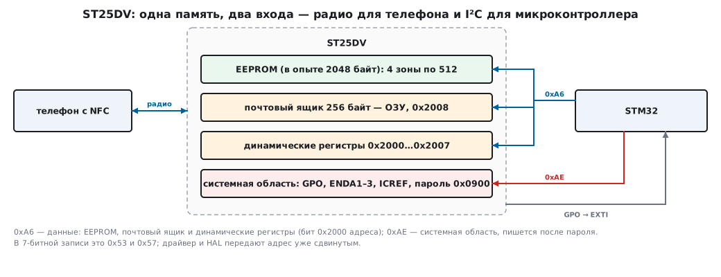
The device has no buttons and no screen, yet you need to configure it: an address, a threshold, a network key. Or the device is broken, and you still want to get its log out. For this there are NFC tags with two inputs. On one side, a phone accesses the tag memory over the radio; on the other, the microcontroller accesses it over I²C. ST25DV is such a tag from ST. This section is about how firmware works with it: which addresses it has on the bus, what lies at which address, why there is a password and how the tag reports that the phone has written something.
The reference values come from the ST25DV driver that ST ships in the support pack for
STM32L4 for Keil (st25dv.c, st25dv.h, st25dv_reg.h). Experiment: this
driver is built unchanged on a PC and connected to a tag model
that prints every I²C transaction. The check is _verify/nfc_st25_check.py.
The radio interface itself is not covered here. For 13.56 MHz, the near field and powering the tag from the reader's field, see section 89.
Terms used in the documentation
Term Meaning dual interface EEPROM an EEPROM with two inputs: radio and wired user memory / user area user memory / a zone of it system configuration area the system area: static settings dynamic register a dynamic register: the current value of a setting, not the stored one fast transfer mode, mailbox fast transfer through a mailbox in RAM GPO — General Purpose Output the tag's interrupt output I2C password, security session the I²C password, the session after it is presented energy harvesting taking energy from outside; in an NFC tag, power from the reader's field brought out to a separate pin for an external circuit
94а.1 Why a tag with two inputs
An ordinary NFC tag is passive memory: the phone writes, the phone reads. ST25DV has a second input, I²C, and its memory is visible to the microcontroller. This gives three typical uses:
- Configuration without buttons. The phone writes parameters into the tag, the firmware reads them at startup or on an interrupt.
- A log from a powered-off device. The firmware stores events in the tag's EEPROM; the phone reads them using the reader's field, even if the device battery is dead.
- Exchanging messages on the fly. The mailbox in the tag's RAM is a buffer of 256 bytes through which the phone and the firmware pass each other short messages without wearing out the EEPROM.
94а.2 Two addresses on the bus and the memory map
The tag answers on the I²C bus at two addresses. Different parts of the memory are visible through them, and the driver picks the address by one bit of the register number:
| Address (8-bit) | 7-bit | What is behind it |
|---|---|---|
0xA6 |
0x53 |
user EEPROM from 0x0000, dynamic registers 0x2000…0x2007, mailbox from 0x2008 |
0xAE |
0x57 |
system area: static settings, tag identity data, password |
The driver's rule for registers: if bit 0x2000 is set in the number, the request goes
to 0xA6, otherwise to 0xAE. The user EEPROM is read and written by separate
driver functions ReadData and WriteData (St25Dv_Drv.ReadData), and they always
go to 0xA6. STM32 HAL and this driver take the address
already shifted left, so the code has 0xA6, while in seven-bit notation
(section 17) the same address is 0x53.
The system area registers you need:
| Register | Address | What it holds |
|---|---|---|
GPO |
0x0000 |
which events to output on the GPO pin |
ENDA1, ENDA2, ENDA3 |
0x0005, 0x0007, 0x0009 |
boundaries of the user memory zones |
I2CSS |
0x000B |
zone protection on the I²C side |
MEM_SIZE |
0x0014–0x0015 |
number of blocks minus one |
BLK_SIZE |
0x0016 |
block size minus one |
ICREF |
0x0017 |
chip code |
UID |
0x0018 |
unique number, 8 bytes |
I2C_PWD |
0x0900 |
window for the password |
Dynamic: GPO_DYN 0x2000, EH_CTRL_DYN 0x2002, RF_MNGT_DYN
0x2003, I2C_SSO_DYN 0x2004 (whether the session is open), IT_STS_DYN 0x2005
(what happened), MB_CTRL_DYN 0x2006 (mailbox enable), MB_LEN_DYN
0x2007.
94а.3 Experiment: the real driver and a tag model
Testing a driver on a real tag means seeing only the outcome: it worked
or it did not. Here it is done differently. The driver files from the pack are built with gcc on
a PC without a single edit, and the bus functions — Read, Write, IsReady,
GetTick, which the driver receives through ST25DV_RegisterBusIO — are
a tag model that prints every transaction: W or R, address, register,
length and bytes.
The model exists only so that the driver has someone to talk to. Its behaviour is defined in the experiment and marked in the output as indented model remarks: an identity of 2048 bytes, a password of eight zeros, three refusals to the ready poll after every EEPROM write, refusal to write the system area without the password. The bytes on the bus are exactly what the driver produced.
The only substitution is an empty cmsis_compiler.h: the PC has no
CMSIS, and the driver needs only stdint.h from it.
94а.4 Identification and size
== 1. Init: опознание
R 0xAE 0x0017 [  1] 26
Init = 0
== 2. объём памяти
R 0xAE 0x0014 [  1] FF
R 0xAE 0x0015 [  1] 01
R 0xAE 0x0016 [  1] 03
Mem_Size = 511, BlockSize = 3 -> 2048 байт
Init reads one byte — ICREF — and compares it with two driver
constants: 0x24 is a 4 Kbit tag, 0x26 is a 16 or 64 Kbit tag. The size
is computed as (MEM_SIZE + 1) × (BLK_SIZE + 1): 512 blocks of 4 bytes —
2048 bytes, that is 16 Kbit.
The same header also has codes 0x25 and 0x27: the macro ST25DV_AM_I_CMOS
calls them CMOS variants, and ST25DV_AM_I_OPEN_DRAIN calls 0x24 and 0x26
open-drain variants. But Init accepts only 0x24 and 0x26:
this driver rejects a CMOS tag during identification.
94а.5 Password and I²C session
The system area holds settings that security depends on: zone boundaries, their protection, the mailbox mode. You can write there only after presenting the password. The driver comments on such functions all say the same thing: the write takes effect only after the I²C password has been presented. In the experiment, the model answered NACK without the password:
== 3. зоны без пароля
W 0xAE 0x0005 [  1] 0F
        модель: NACK — системная область без пароля не пишется
WriteEndZonex = -102
== 4. пароль
W 0xAE 0x0900 [ 17] 00 00 00 00 00 00 00 00 09 00 00 00 00 00 00 00 00
        модель: пароль верный, сессия I2C открыта
        опрос готовности: 1 раз, из них NACK 0
PresentI2CPassword = 0
R 0xA6 0x2004 [  1] 01
сессия = 1
The password is 64 bits. The driver builds a frame of 17 bytes: the password (8 bytes,
most significant byte first), the code 0x09, and the same password once more. Changing the password is
the same frame with the code 0x07, with the new password in both places, and it can be done
only inside an open session. Whether the session is open is shown by the
dynamic register I2C_SSO_DYN (0x2004); -102 is ST25DV_NACK.
A password in firmware is as much a secret as an encryption key: whoever reads it from Flash can reconfigure the tag.
94а.6 Memory zones
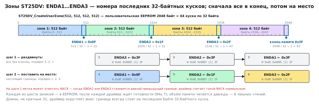
The user EEPROM can be split into four zones, each with
its own protection — separately for radio and for I²C. The boundaries are stored in ENDA1…
ENDA3 in units of 32 bytes: the number of the zone's last 32-byte chunk.
ST25DV_CreateUserZone(512, 512, 512, 512) in the experiment:
W 0xAE 0x0009 [  1] 3F
W 0xAE 0x0007 [  1] 3F
W 0xAE 0x0005 [  1] 3F
W 0xAE 0x0005 [  1] 0F
W 0xAE 0x0007 [  1] 1F
W 0xAE 0x0009 [  1] 2F
First all three boundaries are set to the end of memory: 2048 / 32 − 1 = 0x3F,
in the order 3, 2, 1. Then the real ones are written: 512 / 32 − 1 = 0x0F,
1024 / 32 − 1 = 0x1F, 1536 / 32 − 1 = 0x2F, now in the order 1, 2, 3.
On the first step the tag may answer NACK — when ENDA2 or ENDA3
becomes equal to the previous boundary. The driver comment calls such a
NACK normal, and the function carries on. Lengths that are not multiples of 32 the driver
rounds down.
Each of the six writes goes to EEPROM, and after each one the driver waits for ready
(94а.7). The memory size is read twice along the way: once in
CreateUserZone, the second time in the nested InitEndZone, six
extra reads in total.
94а.7 Writing EEPROM: chunks of 256 bytes and ready polling
== 6. запись 300 байт в EEPROM
W 0xA6 0x0000 [256] 00 01 02 03 04 05 06 07 08 09 0A 0B 0C 0D 0E 0F 10 …
        опрос готовности: 4 раз, из них NACK 3
W 0xA6 0x0100 [ 44] 00 01 02 03 04 05 06 07 08 09 0A 0B 0C 0D 0E 0F 10 …
        опрос готовности: 4 раз, из них NACK 3
WriteData = 0
The tag accepts no more than 256 bytes in one transaction, so
300 bytes went out in two chunks: 256 from address 0x0000 and 44 from 0x0100.
After each chunk the tag spends some time writing the EEPROM and does not answer
at its address. The driver calls IsReady in a loop until it gets an
ACK — this is ready polling (acknowledge polling). The wait limit is ST25DV_WRITE_TIMEOUT
= 320 ms; a comment in the driver derives it as 256 bytes / 4 bytes
per internal page × 5 ms per page. If the tag never answers,
the function returns ST25DV_TIMEOUT.
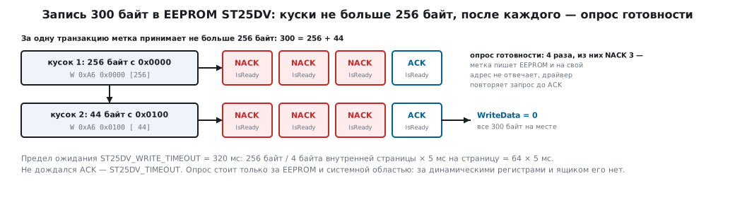
After writes to the dynamic registers and the mailbox the driver does not wait for ready: polling follows only writes to EEPROM and the system area.
94а.8 The mailbox and the GPO pin
== 7. почтовый ящик
R 0xA6 0x2006 [  1] 00
W 0xA6 0x2006 [  1] 01
W 0xA6 0x2008 [ 10] 74 65 6D 70 3D 32 33 2E 35 43
WriteMailboxData = 0
WriteMailboxData(257) = -1
== 8. вывод GPO
W 0xAE 0x0000 [  1] C8
        опрос готовности: 4 раз, из них NACK 3
ConfigIT = 0
ST25DV_SetMBEN_Dyn enables the mailbox in read-modify-write
fashion: it read MB_CTRL_DYN, set the MBEN bit (0x01), and wrote it back.
On a real tag this is not enough: MBEN is set only if fast
transfer is allowed by the static register MB_MODE (0x000D, bit 0), and from the
factory it holds 0 — so the tag does not accept the write to MB_CTRL_DYN. Therefore, once,
after PresentI2CPassword, you call
ST25DV_WriteMBMode(…, ST25DV_ENABLE): this is a write to the system area,
with ready polling, like for GPO. The value is stored in EEPROM, and from then on
SetMBEN_Dyn works at every power-up. The model in the experiment does not emulate this restriction,
so it does not show up in the log.
The message temp=23.5C is 10 bytes from address 0x2008. The driver does not write more than 256 bytes
into the mailbox: for 257 it returned -1 (ST25DV_ERROR) without going
out on the bus.
GPO is a tag pin that you can wire to an EXTI input of the microcontroller
(section 7). The GPO register selects which events toggle it. By the masks
from st25dv_reg.h:
| Bit | Mask | Event |
|---|---|---|
| 0 | 0x01 |
RFUSERSTATE — a state set over the radio |
| 1 | 0x02 |
RFACTIVITY — activity over the radio |
| 2 | 0x04 |
RFINTERRUPT — an interrupt requested over the radio |
| 3 | 0x08 |
FIELDCHANGE — the field appeared or disappeared |
| 4 | 0x10 |
RFPUTMSG — the phone put a message into the mailbox |
| 5 | 0x20 |
RFGETMSG — the phone took a message |
| 6 | 0x40 |
RFWRITE — a write over the radio |
| 7 | 0x80 |
ENABLE — the pin is enabled at all |
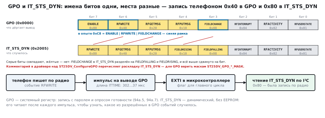
In the experiment 0xC8 = 0x80 | 0x40 | 0x08: the pin is enabled and reacts to
a write by the phone and to the field. GPO is a system register, so it needs
the password and ready polling. After the interrupt the firmware reads IT_STS_DYN
(0x2005) to find out what exactly happened. The pulse duration
is selected in ITTIME from eight values — from 302 down to 37 µs.
94а.9 What the phone sees
A phone without a special app reads from the tag not bytes but an NDEF
message — a standard wrapper for a link, text or an app record.
At the start of the tag memory lies a service file, CC (Capability Container):
from it the phone learns that the tag is formatted for NDEF and how much room
the message has. The driver can forbid writes to the blocks of the CC file — one or two
(LOCKCCFILE, 0x000C) — so that a stray write does not break the formatting.
The byte-level format of CC and NDEF is defined by the NFC Forum specifications; this section does not cover them. In practice a device does this: it gives the first blocks to the CC and an NDEF message (for example, a link to the device's page), and keeps its own data in a separate zone closed to radio writes.
94а.10 Pitfalls
The tag does not answer on I²C while a phone is nearby. The driver comment
on IsDeviceReady says exactly this: during a radio exchange I²C gets
NACK. The firmware must retry the request, not fail with a bus error.
Writing settings "does not work". The system area is not written without the password
(94а.5). First PresentI2CPassword, then everything else.
The wrong address. The code has 0xA6/0xAE, a bus scanner shows 0x53/0x57
(94а.2). The system registers need the second address: there is no single "tag
address".
The comment lies about GPO. Above ST25DV_GetGPOStatus and
ST25DV_ConfigureGPO the driver lists the bits RFBUSY = 0x02,
FIELDFALLING = 0x08, FIELDRISING = 0x10, RFPUTMSG = 0x20,
RFGETMSG = 0x40, RFWRITE = 0x80. This is the layout of IT_STS_DYN, not GPO:
in GPO a write by the phone is 0x40, and 0x80 is the pin enable (94а.8).
Trust the ST25DV_GPO_*_MASK masks.
A CMOS tag fails Init (94а.4): the driver knows its codes, but during
identification compares only with 0x24 and 0x26.
Extra write cycles. EEPROM wears out, while mailbox messages live in RAM. Frequent short exchanges go through the mailbox; to EEPROM only what must survive a power-off.
94а.11 Summary
- ST25DV is an EEPROM with two inputs: the phone over the radio, the microcontroller over I²C.
- There are two addresses on the bus:
0xA6(0x53) — data, dynamic registers and the mailbox;0xAE(0x57) — the system area. The driver picks the address by bit0x2000. - The system area is written only after the password: 17 bytes — password,
0x09, password; changing the password uses the code0x07. - EEPROM is written in chunks of up to 256 bytes with ready polling of up to 320 ms; the mailbox and dynamic registers — without waiting.
- Zones are set by boundaries in units of 32 bytes; the driver first moves them out to the end, then puts them in place.
- GPO to an EXTI input plus
IT_STS_DYN— and the firmware learns about a write by the phone without polling the bus.
Next: section 94б "Flipper Zero inside: STM32WB55, FreeRTOS and 433 MHz radio, NFC, RFID and IR in one firmware" — an open device where four more radio paths work alongside NFC.