 Embedded HandbookApps
57б. Motor current: shunt, amplifier, sampling at the right moment of the PWM
Section 57а drove a motor and on every PWM period it "measured the phase currents" — in a single line. This section shows how that is done: where the shunt goes, how its tens of millivolts are turned into the full ADC scale, at which moment of the period to take the sample so that you get the average current without a filter, and how the same signal shuts the PWM down on overload before the program notices anything.
The built-in op amps and comparators of the G4 are described in section 44, overcurrent protection built on them in 44.8. Here the same blocks work for a motor: a low-side shunt, current of both signs, sampling tied to the PWM.
References: the G474 datasheet (DS12288, table 80 — op amp, ADC characteristics,
absolute maximum ratings) and the reference manual RM0440 (interconnection tables 65,
71, 72, TIM1, ADC and DAC registers) from the Keil pack STM32G4xx_DFP 1.6.0, and the header
stm32g474xx.h from the same pack. The phase current and the amplifier are computed with a model on a PC:
ngspice in the stm-lab:1 image, the op amp macromodel from section 164 with the numbers
from DS12288, directory _verify/mcur57c. The setup code is built with armclang for the
G474. The 2 Ω / 1 mH winding and 12 V are the motor from 57.5; the 10 mΩ shunt is the same as
in 44.8; the 8 A threshold is an example.
Terms used in the documentation
Term Meaning shunt resistor, current sense a low-value resistor that turns current into voltage; current measurement low-side / in-line / single (DC-link) shunt a shunt under the low-side switch / in the phase line / in the common supply rail phase current the current in one motor phase programmable gain amplifier (PGA) with external bias an amplifier with selectable gain and an offset on its input injected channel, JSQR, JEXTSEL the injected ADC channel, its sequence register and its trigger source trigger output 2 (TRGO2, MMS2) the second trigger output of a timer center-aligned PWM PWM with the counter counting up and down trigger conversion latency (tLATR) the delay from the trigger to the start of sampling blanking masking the comparator output while the switches change state break input (BKIN, tim_brk_cmp) the emergency shutdown input of a timer
57б.1 Where to put the shunt
| Location | What it sees | Common-mode voltage on the shunt | What amplifies it |
|---|---|---|---|
| low side, a shunt under each low-side switch | the phase current while the low-side switch is on | near zero | the built-in G4 op amp |
| in the phase line, between the bridge and the winding | the phase current at all times | jumps from 0 to 12 V on every PWM edge | an external amplifier rated for that common-mode voltage |
| in the common rail, one per bridge | in each switch state, the current of one of the phases or zero | near zero | the built-in op amp, but the phase currents must be reconstructed from two samples per period |
The built-in G4 op amp accepts only 0…VDDA on its inputs (DS12288, table 80), so a shunt in the phase line is beyond it. A common shunt saves parts, but it requires shifting the PWM edges so that there is time to measure — a separate topic not covered here. From here on: a low-side shunt, 10 mΩ.
A low-side shunt has two properties, and the whole section follows from them. First: current flows through it only while the low-side switch is on — so the sample must be taken exactly then. Second: the sign. Current that flows out of the phase into the winding goes through the shunt from bottom to top, from ground, while the low-side switch is on — the voltage on the shunt is negative. In the model, at +1.5 A the shunt shows −14.992 mV, at −1.5 A it shows +15.006 mV. The amplifier needs both signs.
57б.2 Current ripple and where to take the sample
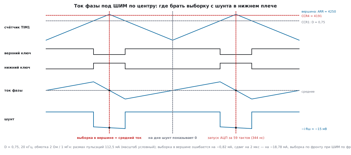
The model is one bridge phase at 12 V: a 2 Ω / 1 mH winding (the motor from 57.5) to a 6 V midpoint that stands in for the neutral of a three-phase motor. Center-aligned PWM at 20 kHz: the TIM1 counter counts up and down, the high-side switch is on around the "bottom" of the counter, the low-side one around the top. For comparison, the same current with edge-aligned PWM. ngspice computes 10 ms, and the last period is taken.
| D | Average current | Ripple, peak to peak | Sampling error at the top | Sampling error at the edge |
|---|---|---|---|---|
| 0.25 | −1.5000 A | 112.5 mA | −0.58 mA | −55.8 mA |
| 0.5 | 0 | 150.0 mA | −0.93 mA | −75.0 mA |
| 0.75 | +1.5000 A | 112.5 mA | −0.82 mA | −56.7 mA |
| 0.9 | +2.4000 A | 54.0 mA | −0.42 mA | −27.4 mA |
The 150 mA ripple at D = 0.5 is the same as in 57.5. What matters is in the last two columns. On each interval the current changes almost along a straight line, and for a straight line segment the midpoint equals the average. The middle of the low-side on-time is the counter top, and a sample there gives the average current over the period with an error below one milliampere — without any filter. The remaining error comes from the fact that, because of the winding resistance, the current follows an exponential rather than a straight line.
A sample at the edge — with edge-aligned PWM, at the counter update — lands on the kink of the ripple: the error is half the peak-to-peak ripple, up to 75 mA. On top of that, the edge is the moment the switches change state, and at that time the shunt shows a spike (section 44.6, blanking).
At the counter bottom, in the middle of the high-side on-time, the current also equals the
average, but the low-side shunt shows zero: no current flows through it. Hence the
trap with triggering on the counter update. In center-aligned mode
with RCR = 0 the update happens both at the top and at the bottom (RM0440:
the repetition counter decrements on both overflow and underflow) —
every second sample will be zero.
57б.3 Triggering the ADC from TIM1: TRGO2 and the sampling offset
You need to trigger once per period and slightly before the top. For
this TIM1 has a second trigger output TRGO2 with the MMS2 field in CR2: code 0111
puts tim_oc4refc on it — the reference signal of the fourth channel, which is not
connected to any pin. Channel 4 in PWM mode 2 is active while the counter is above
CCR4 — a pulse around the top, and its rising edge triggers the ADC. According to table
65 of RM0440, source 8 for the injected channels of ADC1/2 is tim1_trgo2.
How much before the top? The numbers for 170 MHz:
| What | Value |
|---|---|
| TIM1 center-aligned, 20 kHz | ARR = 4250: up and down — 8500 clocks, 50 µs |
| ADC clock | HCLK/4 = 42.5 MHz, CKMODE = 11 |
delay from trigger to sampling, tLATR |
at most 2.125 ADC clocks — 50.0 ns (DS12288, CKMODE = 11) |
| sampling | 12.5 clocks — 294.1 ns |
| trigger before the top | 344.1 ns — 59 TIM1 clocks: CCR4 = 4191 |
Sampling ends exactly at the top: after that the ADC converts the voltage it is already holding. The ADC clock is taken synchronous, from HCLK: according to RM0440, in the synchronous modes the delay from a timer trigger has no jitter, and 59 clocks are always 59.
And if you get it wrong? The sampling error for an offset after the top, based on what the ADC sees on the shunt:
| Offset | D = 0.75 | D = 0.9 |
|---|---|---|
| 0.344 µs | −3.91 mA | −4.14 mA |
| 1 µs | −9.81 mA | −11.21 mA |
| 2 µs | −18.78 mA | −21.98 mA |
| 5 µs | −45.58 mA | −2400.00 mA |
The error is the current slope at the top (−9.00 A/ms at D = 0.75) times the offset. Ignoring the delay and the sampling time altogether costs 344 ns — a few milliamperes at a current of one and a half amperes. The real danger is elsewhere: at D = 0.9 the low-side switch is on for only 5 µs, and an offset of 5 µs moves the sample out of the window — the ADC sees zero instead of 2.4 A.
    TIM1->PSC = 0;
    TIM1->ARR = PWM_ARR;
    TIM1->CR1 = (1u << TIM_CR1_CMS_Pos) | TIM_CR1_ARPE;       /* вверх-вниз, режим 1 */
    TIM1->CCR4 = PWM_CCR4;
    TIM1->CCMR2 = (TIM1->CCMR2 & ~(TIM_CCMR2_OC4M_Msk | TIM_CCMR2_CC4S_Msk))
                | (OC_PWM2 << TIM_CCMR2_OC4M_Pos) | TIM_CCMR2_OC4PE;
    TIM1->CR2 = (TIM1->CR2 & ~TIM_CR2_MMS2_Msk) | (MMS2_OC4REFC << TIM_CR2_MMS2_Pos);

    ADC12_COMMON->CCR = (ADC12_COMMON->CCR & ~ADC_CCR_CKMODE_Msk) | (CKMODE_HCLK_4 << ADC_CCR_CKMODE_Pos);
    ADC1->SMPR2 = (ADC1->SMPR2 & ~ADC_SMPR2_SMP12_Msk) | (SMP_12_5 << ADC_SMPR2_SMP12_Pos);
    ADC1->JSQR = (0u << ADC_JSQR_JL_Pos)                      /* одно преобразование */
               | (JEXTSEL_T1TRGO2 << ADC_JSQR_JEXTSEL_Pos)
               | (JEXTEN_RISING << ADC_JSQR_JEXTEN_Pos)
               | (12u << ADC_JSQR_JSQ1_Pos);                  /* ADC1_IN12 — PB1 */
The injected channel is convenient because it lives apart from the regular sequence:
scanning the other channels with DMA (section 14.6) runs on its own, and
the current sample interrupts it at the scheduled moment. Enabling the ADC — the regulator,
calibration, ADEN — is as in 15а.3.
57б.4 Amplifier: PGA −15 with a bias from DAC3
The shunt carries ±0.1 V, while the ADC needs a 0…3.3 V scale with zero current in the middle. This
is done by OPAMP3 in PGA mode with inverting gain and a bias
(RM0440, the section on PGA mode with external bias): the shunt goes to the VINM0 pin
(PB2) through the internal resistor R1, and the "+" input gets the voltage from DAC3_CH2.
For the inverting configuration with the ×16 divider:
Uout = 16·Ubias − 15·Ushunt.
A DAC3 bias of code 128 is 3.3 · 128 / 4096 = 0.103125 V, and at zero current the output is exactly 1.65 V. Current out of the phase gives a negative Ushunt — the output rises; reverse current makes it fall. The output does not come closer than 0.1 V to the rails (DS12288), so the scale is ±10.33 A. The step is 0.806 mV per ADC code, which is 5.37 mA.
Why inverting. In this configuration the inputs of the op amp itself sit at the 0.103 V bias,
inside the allowed 0…VDDA, and the shunt sees only the VINM0 pin through a
10 kΩ resistor. The −0.1 V on the pin is within the absolute
maximum of VSS − 0.3 V (DS12288). In the non-inverting configuration the shunt would go
straight to the op amp input, and the negative sign of the current would be out of range.
What the model says (ngspice, R1 = 10 kΩ, R2 = 150 kΩ from table 80,
open-loop gain 95 dB): at zero current 1.6498 V, at −0.1 V on the
shunt 3.1493 V, gain 14.996. Each resistor has a spread of ±15 %, but
the datasheet holds the −15 gain within ±1 %. The op amp offset of ±1.5 mV (44.2) is
multiplied by 16 at the output: ±24 mV, that is ±160 mA. That is why the zero code
code_zero is taken with the motor standing still and subtracted from every sample.
    DAC3->MCR = (DAC_MODE_INT << DAC_MCR_MODE1_Pos) | (DAC_MODE_INT << DAC_MCR_MODE2_Pos)
              | DAC_MCR_HFSEL_1;                             /* AHB 170 МГц */
    DAC3->DHR12R1 = DAC_TRIP;
    DAC3->DHR12R2 = DAC_BIAS;
    DAC3->CR |= DAC_CR_EN1 | DAC_CR_EN2;

    OPAMP3->CSR = (VPSEL_DAC << OPAMP_CSR_VPSEL_Pos)          /* «+» — смещение 0,103 В */
                | (VMSEL_PGA << OPAMP_CSR_VMSEL_Pos)
                | (PGA_INV_15 << OPAMP_CSR_PGGAIN_Pos)        /* выход = 16·Uсм − 15·Uш */
                | OPAMP_CSR_OPAMPxEN;                         /* выход на PB1: и в АЦП, и в COMP1 */
Why OPAMP3. According to tables 71 and 72 of RM0440 its output is PB1, and PB1 is
both the ADC input ADC1_IN12 and the "+" input of comparator COMP1. One signal goes to both
the controller and the protection. The bias is DAC3_CH2: of all DAC channels, it is the only one
OPAMP3 has on its "+" input. DAC mode 011 — output to internal blocks only, no buffer.
Converting the code to milliamperes — with integers:
static inline int32_t phase_mA(uint16_t code, uint16_t code0)
{
    return ((int32_t)code - (int32_t)code0) * 22000 / 4095;
}
The function was built with gcc on a PC and checked against the model: 1.5 A is code 2327 and 1498 mA, −10 A is code 186 and −10003 mA.
57б.5 Measurement window and filter
When the low-side switch turns on, the shunt sees a step — from zero to −i·Rshunt, and the op amp output must settle to it before sampling. The model is a step of −0.1 V (10 A); the output swings 1.5 V and must settle to within half an ADC code, 0.403 mV:
| Op amp | GBW, slew rate | Settling | Low-side switch on at least | Maximum D |
|---|---|---|---|---|
| typical | 13 MHz, 6.5 V/µs | 1.01 µs | 2.61 µs | 0.948 |
| worst case per the datasheet | 7 MHz, 2.5 V/µs | 2.46 µs | 5.51 µs | 0.890 |
The window is calculated like this: sampling ends at the top, so from the moment the low-side switch turns on to the start of sampling there is half of its on-time minus the sampling time, and the settling has to fit in there. At a higher duty cycle the current of this phase cannot be measured in this period. For three phases this is not a problem: two currents are enough (57а.7), and the phase with the highest duty cycle has the shortest low-side on-time of all — that is the one computed from the other two. The dead time narrows the window further — calculate with the real edges.
Filter. A hardware RC is practically impossible here. In PGA mode the
capacitor goes on the VINM1 pin in parallel with R2 = 150 kΩ, and its
time constant must fit into the window with a margin for settling to
half a code — ln(8190) times: at D = 0.9 the window is 2.206 µs, the time constant at most
0.245 µs, the capacitor at most 1.63 pF. The filter is the mid-point
sampling itself: it already gives the average current. The controller smooths out the rest of the noise.
57б.6 Overcurrent protection: COMP1 shuts the PWM down
The same op amp output on PB1 goes to the "+" input of COMP1; the threshold is DAC3_CH1. A current out of the phase of 8 A is 1.65 + 15 · 0.01 · 8 = 2.85 V at the output, DAC code 2.85 / 3.3 · 4096 = 3537; with this code the threshold is 7.9976 A. The hysteresis of 20 mV at the op amp output is 133 mA of current.
    COMP1->CSR = (INM_DAC3_CH1 << COMP_CSR_INMSEL_Pos)
               | (INP_PB1 << COMP_CSR_INPSEL_Pos)
               | (HYST_20MV << COMP_CSR_HYST_Pos)
               | (BLANK_TIM1_OC5 << COMP_CSR_BLANKING_Pos)    /* выброс при переключении не считается */
               | COMP_CSR_EN;
    TIM1->AF1 |= TIM1_AF1_BKCMP1E;
    TIM1->BDTR |= TIM_BDTR_BKP | TIM_BDTR_BKE;               /* авария — единицей (раздел 44.8) */
Through BKCMP1E the comparator output reaches the TIM1 break input, and
MOE is cleared without the core (57а.6). The BKP polarity and blanking
with the TIM1 OC5 pulse are as in 44.6 and 44.8.
Two caveats. The comparator here catches only current out of the phase — the op amp output above the threshold. Reverse current drives the output down, and that needs a second comparator; in table 71 PB1 is an input of COMP1 only, so the op amp output is routed to the second comparator by a trace on the board. And most importantly: the low-side shunt is blind while the high-side switch is on — it will not see a phase short to ground during that time. Against such a short you need a shunt in the common rail or the protection of the gate driver.
57б.7 Pitfalls
Every second sample is zero. The ADC is triggered by the TIM1 update in
center-aligned mode with RCR = 0: the update happens both at the top and at the bottom, and at the bottom
the low-side switch is off. Trigger from TRGO2 on the OC4REF edge, once per
period.
The current "drifts" by half the ripple. The sample is taken at the PWM edge: an error of up to 75 mA in the model. Sample in the middle of the low-side on-time.
At high duty cycle the phase current is zero or garbage. The low-side switch is on for less time than the amplifier needs to settle: 2.61 µs for a typical op amp, 5.51 µs for the worst case. Compute this phase from the other two.
The current with the motor standing still is not zero. The op amp offset ×16 is up to ±160 mA. Take the zero code when stopped and subtract it.
The current sign is inverted. Current out of the phase makes the low-side shunt negative; the inverting PGA restores the sign. In the non-inverting configuration the negative voltage goes beyond the op amp input range.
A capacitor "against noise" in the PGA feedback. Already 1.63 pF with R2 = 150 kΩ eats the whole window at D = 0.9.
The protection did not trip on a short to ground. The low-side shunt does not see current while the high-side switch is on. You need a second line of protection.
The protection threshold is calculated from 1.65 V, but the zero has drifted. The threshold is a DAC code; it knows nothing about the op amp offset. The threshold margin must cover ±160 mA.
57б.8 Summary
- Low-side shunt — 10 mΩ, common-mode voltage near zero, the built-in op amp handles it; the current is visible only while the low-side switch is on, and current out of the phase gives a negative voltage on the shunt.
- Center-aligned PWM and a sample at the counter top give the average current: an error below 1 mA versus 27…75 mA for a sample at the edge.
- Trigger:
TRGO2=OC4REF(MMS2= 0111), injected channel of ADC1 with source 8;CCR4= 4191 withARR= 4250 — 344 ns before the top. - OPAMP3 in PGA −15 mode with a DAC3 bias of code 128: zero current is 1.65 V, scale ±10.33 A, 5.37 mA per code; the op amp offset of up to ±160 mA is removed by zero calibration.
- Settling after the low-side switch turns on is 1.01…2.46 µs: maximum duty cycle 0.948 for a typical op amp and 0.890 for the worst case.
- COMP1 with threshold 3537 (8 A) shuts the PWM down through
BKCMP1Ewithout the core; the low-side shunt is blind while the high-side switch is on.
Full source code
mc57c.c — phase current on the STM32G474: PGA, sampling by TIM1, COMP1 protection.
/* 57б: ток фазы на STM32G474 — шунт в нижнем плече, OPAMP3 в режиме PGA −15 со смещением от DAC3,
   выборка инжектированным каналом ADC1 по TIM1 TRGO2 в вершине счётчика, защита COMP1 → авария TIM1.
   Шунт — на PB2 (OPAMP3_VINM0), выход ОУ — PB1: он же ADC1_IN12 и COMP1_INP (RM0440, табл. 71 и 72).
   Собирается armclang: -DSTM32G474xx -include stm32g4xx.h. */
#include <stdint.h>
#include "mc57c.h"

/* ── биты, на которые опирается код: из заголовка пака ───────────────── */
_Static_assert(TIM_CR2_MMS2_Pos == 20u && TIM_CR2_MMS2_Msk == (0xFu << 20), "MMS2 — биты 23:20 TIMx_CR2");
_Static_assert(ADC_JSQR_JL_Pos == 0u && ADC_JSQR_JEXTSEL_Pos == 2u && ADC_JSQR_JEXTEN_Pos == 7u && ADC_JSQR_JSQ1_Pos == 9u,
               "JSQR: JL, JEXTSEL, JEXTEN, JSQ1");
_Static_assert(ADC_CCR_CKMODE_Pos == 16u && ADC_SMPR2_SMP12_Pos == 6u, "CKMODE — 17:16 CCR, SMP12 — 8:6 SMPR2");
_Static_assert(OPAMP_CSR_VPSEL_Pos == 2u && OPAMP_CSR_VMSEL_Pos == 5u && OPAMP_CSR_PGGAIN_Pos == 14u, "OPAMP_CSR");
_Static_assert(COMP_CSR_INMSEL_Pos == 4u && COMP_CSR_INPSEL_Pos == 8u && COMP_CSR_HYST_Pos == 16u
               && COMP_CSR_BLANKING_Pos == 19u, "COMP_CSR");
_Static_assert(DAC_MCR_MODE1_Pos == 0u && DAC_MCR_MODE2_Pos == 16u, "DAC_MCR: MODE1, MODE2");
_Static_assert(TIM_CCMR2_OC4M_Pos == 12u, "OC4M[2:0] — биты 14:12 CCMR2");

#define MMS2_OC4REFC    7u      /* 0111: tim_oc4refc — на tim_trgo2 */
#define JEXTSEL_T1TRGO2 8u      /* ADC1/2, инжектированные: 8 — tim1_trgo2 */
#define JEXTEN_RISING   1u
#define CKMODE_HCLK_4   3u      /* синхронно, HCLK/4 = 42,5 МГц: без дрожания от запуска таймером */
#define SMP_12_5        2u      /* 12,5 такта = 294 нс */
#define OC_PWM2         7u      /* 0111: вверх — активен при CNT > CCR, вниз — при CNT > CCR */
#define VPSEL_DAC       3u      /* у OPAMP3 — DAC3_CH2 */
#define VMSEL_PGA       2u
#define PGA_INV_15      11u     /* 01011: −15, вход через R1 с VINM0 (PB2) */
#define DAC_MODE_INT    3u      /* 011: только на внутренние блоки, без буфера */
#define INM_DAC3_CH1    4u      /* у COMP1 — DAC3_CH1 (раздел 44.6) */
#define INP_PB1         1u      /* второй вход COMP1: PB1 */
#define HYST_20MV       2u
#define BLANK_TIM1_OC5  1u
_Static_assert(PGA_INV_15 == (8u | 3u), "+8 — инвертирующее с VINM0, 3 — делитель ×16");
_Static_assert(PWM_CCR4 == 4191u && DAC_BIAS == 128u && DAC_TRIP == 3537u, "числа — из модели");

/* Усилитель и опоры: DAC3_CH2 — смещение, DAC3_CH1 — порог защиты. */
void current_amp_init(void)
{
    RCC->AHB2ENR |= RCC_AHB2ENR_GPIOBEN | RCC_AHB2ENR_DAC3EN | RCC_AHB2ENR_ADC12EN;
    RCC->APB2ENR |= RCC_APB2ENR_SYSCFGEN | RCC_APB2ENR_TIM1EN;
    GPIOB->MODER |= (3u << (1 * 2)) | (3u << (2 * 2));        /* PB1, PB2 — аналоговые */

    DAC3->MCR = (DAC_MODE_INT << DAC_MCR_MODE1_Pos) | (DAC_MODE_INT << DAC_MCR_MODE2_Pos)
              | DAC_MCR_HFSEL_1;                             /* AHB 170 МГц */
    DAC3->DHR12R1 = DAC_TRIP;
    DAC3->DHR12R2 = DAC_BIAS;
    DAC3->CR |= DAC_CR_EN1 | DAC_CR_EN2;

    OPAMP3->CSR = (VPSEL_DAC << OPAMP_CSR_VPSEL_Pos)          /* «+» — смещение 0,103 В */
                | (VMSEL_PGA << OPAMP_CSR_VMSEL_Pos)
                | (PGA_INV_15 << OPAMP_CSR_PGGAIN_Pos)        /* выход = 16·Uсм − 15·Uш */
                | OPAMP_CSR_OPAMPxEN;                         /* выход на PB1: и в АЦП, и в COMP1 */
}

/* ШИМ по центру и запуск АЦП в вершине счётчика — в середине открытого нижнего ключа. */
void pwm_adc_sync_init(void)
{
    TIM1->PSC = 0;
    TIM1->ARR = PWM_ARR;
    TIM1->CR1 = (1u << TIM_CR1_CMS_Pos) | TIM_CR1_ARPE;       /* вверх-вниз, режим 1 */
    TIM1->CCR4 = PWM_CCR4;
    TIM1->CCMR2 = (TIM1->CCMR2 & ~(TIM_CCMR2_OC4M_Msk | TIM_CCMR2_CC4S_Msk))
                | (OC_PWM2 << TIM_CCMR2_OC4M_Pos) | TIM_CCMR2_OC4PE;
    TIM1->CR2 = (TIM1->CR2 & ~TIM_CR2_MMS2_Msk) | (MMS2_OC4REFC << TIM_CR2_MMS2_Pos);

    ADC12_COMMON->CCR = (ADC12_COMMON->CCR & ~ADC_CCR_CKMODE_Msk) | (CKMODE_HCLK_4 << ADC_CCR_CKMODE_Pos);
    ADC1->SMPR2 = (ADC1->SMPR2 & ~ADC_SMPR2_SMP12_Msk) | (SMP_12_5 << ADC_SMPR2_SMP12_Pos);
    ADC1->JSQR = (0u << ADC_JSQR_JL_Pos)                      /* одно преобразование */
               | (JEXTSEL_T1TRGO2 << ADC_JSQR_JEXTSEL_Pos)
               | (JEXTEN_RISING << ADC_JSQR_JEXTEN_Pos)
               | (12u << ADC_JSQR_JSQ1_Pos);                  /* ADC1_IN12 — PB1 */
    ADC1->IER |= ADC_IER_JEOCIE;
    /* включение АЦП (регулятор, калибровка, ADEN) — раздел 15а; затем: */
    ADC1->CR |= ADC_CR_JADSTART;
    NVIC_EnableIRQ(ADC1_2_IRQn);
}

/* Перегрузка: COMP1 сравнивает выход ОУ с порогом и через аварийный вход гасит ШИМ. */
void overcurrent_init(void)
{
    COMP1->CSR = (INM_DAC3_CH1 << COMP_CSR_INMSEL_Pos)
               | (INP_PB1 << COMP_CSR_INPSEL_Pos)
               | (HYST_20MV << COMP_CSR_HYST_Pos)
               | (BLANK_TIM1_OC5 << COMP_CSR_BLANKING_Pos)    /* выброс при переключении не считается */
               | COMP_CSR_EN;
    TIM1->AF1 |= TIM1_AF1_BKCMP1E;
    TIM1->BDTR |= TIM_BDTR_BKP | TIM_BDTR_BKE;               /* авария — единицей (раздел 44.8) */
}

volatile uint16_t code_zero = 2048;                           /* снимается при стоящем двигателе */
volatile int32_t i_phase_mA;

void ADC1_2_IRQHandler(void)
{
    ADC1->ISR = ADC_ISR_JEOC;
    i_phase_mA = phase_mA((uint16_t)ADC1->JDR1, code_zero);
}
Next: section 57в "VESC and OpenInverter: power electronics controlled over CAN" — how to command motor controllers and inverters over the bus.