 Embedded HandbookApps
2г. Milandr K1986VE92: a domestic Cortex-M3 next to the STM32
Section 1.9 put the K1986VE9x next to the STM32F103 in one table, and 8.7 said in one sentence that its ports are organised differently. Here it is in detail: what changes in the code when a program for the F103 is ported to the K1986VE92QI. The core is the same, a Cortex-M3, but the clocking, the ports, peripheral enabling and the library are its own. It is chosen when a product needs a domestic component base and acceptance inspection.
Prerequisites: the Milandr.MDR32FxQI 1.3.2 pack for Keil — the device description (pdsc),
the header MDR32F9Q2I.h (this is what the K1986VE92QI is called in the library),
the SPL MDR32FxQI 1.3.0 library and the examples RST_CLK/CPU_Clock and
PORT/Joystick_LEDs; the same files lie unchanged in MDR32_SPL_v1.5.0.
STM32F103 — the Keil pack STM32F1xx_DFP 2.4.1. The LED blink is built with
armclang in four variants, the core frequency is computed by the pack functions on a PC.
QEMU does not model this microcontroller, and nothing was run on a board.
Terms used in the documentation
Term Meaning RST_CLK the reset and clock block — the counterpart of RCC CPU_C1, CPU_C2, CPU_C3 the three stages of core clock selection: source, PLL, divider HCLK_SEL the switch that selects where the core clock comes from PER_CLOCK the peripheral clock enable register, one for all blocks PORT: RXTX, OE, FUNC, ANALOG, PWR data, direction, function, digital mode, pin driver MDR_EEPROM Milandr's controller of the on-chip Flash memory (the block is named EEPROM) DUcc the built-in core voltage regulator SSP synchronous serial port — this is SPI
2г.1 One core, different peripherals
The descriptions from the Keil packs:
| K1986VE92QI (MDR32F9Q2I) | STM32F103C8 | |
|---|---|---|
| core | Cortex-M3 r2p0, has an MPU | Cortex-M3 |
| frequency | up to 80 MHz | up to 72 MHz |
| Flash | 128 KB from address 0x0800 0000 | 64 KB from address 0x0800 0000 |
| RAM | 32 KB from address 0x2000 0000 | 20 KB from address 0x2000 0000 |
| oscillators | HSI 8 MHz, LSI 40 kHz, external HSE 2…16 MHz | not given in the pack description |
| NVIC priority bits | 3 | 4 |
The memory map is the same: Flash and RAM are in the same place, the peripherals also start at 0x4000 0000,
there is bit-banding (PERIPH_BB_BASE = 0x4200 0000). The core registers, SysTick,
the NVIC and the instruction set itself are the same. But already the number of priority bits is not
a property of the core but a decision of the chip vendor: 3 against 4. Beyond that,
everything that lies past address 0x4000 0000 diverges.
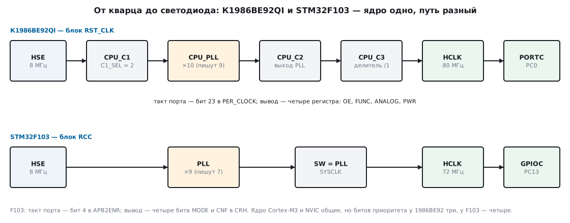
2г.2 Clocking: RST_CLK instead of RCC
The RST_CLK block is at address 0x4002 0000. The registers needed: CLOCK_STATUS
(0x00, ready flags), PLL_CONTROL (0x04), HS_CONTROL (0x08, the crystal),
CPU_CLOCK (0x0C) and PER_CLOCK (0x1C). The core clock passes through three stages:
CPU_C1— the source: HSI, HSI/2, HSE, HSE/2 (theC1_SELfield, values 0…3);CPU_C2—CPU_C1as is or theCPU_PLLoutput;CPU_C3— the divider: values 0…7 mean division by 1, 8 by 2, 9 by 4 and so on up to 15 — by 256.
The final switch HCLK_SEL selects what goes to the core: HSI,
CPU_C3, LSE or LSI. The PLL multiplier is written as "N − 1": ×10
is 9 (on the F103 ×9 is written as 7).
Before raising the clock to 80 MHz two more steps are needed that the F103 either does not have or
does differently. The Flash read latency is set in the controller named
EEPROM: according to the SPL comments, 2 cycles — up to 75 MHz, 3 — up to 100 MHz, so
80 MHz needs 3. And the built-in core regulator DUcc (a field in BKP->REG_0E)
is switched to the "up to 80 MHz" mode — value 6. The CPU_Clock example sets
the Flash latency before raising the frequency. All of it at register level:
void mdr_clock_80mhz(void)
{
    MDR_RST_CLK->PER_CLOCK |= RST_CLK_PER_CLOCK_PCLK_EN_EEPROM    /* иначе не записать CMD */
                            | RST_CLK_PER_CLOCK_PCLK_EN_BKP;      /* и REG_0E */
    MDR_RST_CLK->HS_CONTROL = RST_CLK_HS_CONTROL_HSE_ON;          /* кварц 8 МГц */
    while ((MDR_RST_CLK->CLOCK_STATUS & RST_CLK_CLOCK_STATUS_HSE_RDY) == 0) { }

    MDR_RST_CLK->CPU_CLOCK = 2u << RST_CLK_CPU_CLOCK_CPU_C1_SEL_Pos;   /* CPU_C1 = HSE, ядро пока от HSI */
    MDR_RST_CLK->PLL_CONTROL = (9u << RST_CLK_PLL_CONTROL_PLL_CPU_MUL_Pos)   /* x10 */
                             | RST_CLK_PLL_CONTROL_PLL_CPU_ON;
    while ((MDR_RST_CLK->CLOCK_STATUS & RST_CLK_CLOCK_STATUS_PLL_CPU_RDY) == 0) { }

    MDR_EEPROM->CMD = 3u << EEPROM_CMD_DELAY_Pos;                 /* Flash: 3 такта, до 100 МГц */
    MDR_BKP->REG_0E = (MDR_BKP->REG_0E & ~(BKP_REG_0E_LOW_Msk | BKP_REG_0E_SELECTRI_Msk))
                    | (6u << BKP_REG_0E_LOW_Pos) | (6u << BKP_REG_0E_SELECTRI_Pos);  /* регулятор: до 80 МГц */

    MDR_RST_CLK->CPU_CLOCK = (2u << RST_CLK_CPU_CLOCK_CPU_C1_SEL_Pos)  /* C1 = HSE */
                           | RST_CLK_CPU_CLOCK_CPU_C2_SEL               /* C2 = выход PLL */
                           | (0u << RST_CLK_CPU_CLOCK_CPU_C3_SEL_Pos)   /* C3 = C2 / 1 */
                           | (1u << RST_CLK_CPU_CLOCK_HCLK_SEL_Pos);    /* HCLK = CPU_C3 */
}
The first write to CPU_CLOCK prepares CPU_C1 but leaves the core on HSI;
the last one switches everything at once. The result is 8 MHz × 10 = 80 MHz, 0x106 in
CPU_CLOCK.
2г.3 Ports: four registers instead of CRL and CRH
On the F103 the pin mode is four bits MODE and CNF in CRL or CRH. On the
K1986VE92 a port is eight registers in a row: RXTX (0x00), OE (0x04),
FUNC (0x08), ANALOG (0x0C), PULL, PD, PWR (0x18) and GFEN.
Each property of a pin is in its own register:
OE: 1 — output, 0 — input;FUNC: two bits per pin, 00 — port, 01 — main function, 10 — alternate, 11 — redefined; there is no separate AFIO block;ANALOG: 1 — digital, 0 — analog;PWR: two bits per pin, 00 — driver off, 01 — slow edge, 10 — fast, 11 — fastest.
The VD3 LED of the development board is on PC0 (the description of the
PORT/Joystick_LEDs example):
void mdr_led_init(void)
{
    MDR_RST_CLK->PER_CLOCK |= RST_CLK_PER_CLOCK_PCLK_EN_PORTC;    /* без такта порт не отвечает */
    MDR_PORTC->OE     |=  (1u << LED_PIN);                        /* 1 — выход */
    MDR_PORTC->FUNC   &= ~PORT_FUNC_MODE0_Msk;                    /* 00 — функция «порт» */
    MDR_PORTC->ANALOG |=  (1u << LED_PIN);                        /* 1 — цифровой, 0 — аналоговый */
    MDR_PORTC->PWR     = (MDR_PORTC->PWR & ~PORT_PWR0_Msk)
                       | (1u << PORT_PWR0_Pos);                   /* 01 — драйвер включён, медленный фронт */
}

void mdr_led_toggle(void)
{
    MDR_PORTC->RXTX ^= (1u << LED_PIN);       /* чтение-изменение-запись: регистра вроде BSRR нет */
}
The same on the F103 (section 8.4, PC13 of the BluePill board):
void f103_led_init(void)
{
    RCC->APB2ENR |= RCC_APB2ENR_IOPCEN;                       /* такт порта C */
    GPIOC->CRH = (GPIOC->CRH & ~(GPIO_CRH_MODE13 | GPIO_CRH_CNF13))
               | GPIO_CRH_MODE13_1;                           /* выход 2 МГц, двухтактный */
}
The K1986VE92 port has no atomic set and reset register like BSRR:
the structure has exactly eight registers, and the SPL function PORT_SetBits for this
model does a read-modify-write of RXTX. The library uses the SETTX and CLRTX registers
only on other models of the series.
The debug pins share the ports: JTAG_A — PB0…PB4, JTAG_B —
PD0…PD4. The SPL protects them with a mask on every write to the port, but only
the interface selected in MDR32FxQI_config.h; by default JTAG_B is
enabled there.
2г.4 PER_CLOCK and the block correspondence table
On the F103 the peripheral clock is enabled by three registers — AHBENR, APB1ENR,
APB2ENR. On the K1986VE92 by one, PER_CLOCK, and the bit number in it matches
bits 19:15 of the block's base address. The SPL computes it exactly that way: the macro
PCLK_BIT(BASE) is 1 << ((BASE >> 15) & 0x1F). Port C at address
0x400B 8000 is bit 23. After RST_CLK_DeInit() only RST_CLK itself and BKP
are enabled in PER_CLOCK, everything else is disabled.
The correspondence of blocks from the two headers:
| STM32F103 | Address | Clock | K1986VE92 | Address | PER_CLOCK bit |
|---|---|---|---|---|---|
| RCC | 0x4002 1000 | — | RST_CLK | 0x4002 0000 | 4 |
| FLASH | 0x4002 2000 | — | EEPROM | 0x4001 8000 | 3 |
| GPIOC | 0x4001 1000 | APB2ENR, bit 4 | PORTC | 0x400B 8000 | 23 |
| AFIO | 0x4001 0000 | APB2ENR, bit 0 | none, the function is in the port's FUNC |
— | — |
| USART1 | 0x4001 3800 | APB2ENR, bit 14 | UART1 | 0x4003 0000 | 6 |
| SPI1 | 0x4001 3000 | APB2ENR, bit 12 | SSP1 | 0x4004 0000 | 8 |
| I2C1 | 0x4000 5400 | APB1ENR, bit 21 | I2C | 0x4005 0000 | 10 |
| TIM1 | 0x4001 2C00 | APB2ENR, bit 11 | TIMER1 | 0x4007 0000 | 14 |
| ADC1 | 0x4001 2400 | APB2ENR, bit 9 | ADC | 0x4008 8000 | 17 |
| CAN1 | 0x4000 6400 | APB1ENR, bit 25 | CAN1 | 0x4000 0000 | 0 |
| DMA1 | 0x4002 0000 | AHBENR, bit 0 | DMA | 0x4002 8000 | 5 |
| BKP | 0x4000 6C00 | APB1ENR, bit 27 | BKP | 0x400D 8000 | 27 |
| IWDG | 0x4000 3000 | — | IWDG | 0x4006 8000 | 13 |
| not in the header | — | — | COMP | 0x4009 8000 | 19 |
Not a single address matches in meaning, but one matches numerically:
0x4002 0000 is DMA1 on the F103 and RST_CLK on the K1986VE92. Code with "hard-coded"
addresses will not fail at build time, but will silently write to the wrong block.
The header MDR32F9Q2I.h also contains an outright error: the macro
RST_CLK_PER_CLOCK_PCLK_EN_COMP refers to a non-existent
RST_CLK_PER_CLOCK_PCLK_EN_TIMER4_Msk, and the line
PER_CLOCK |= RST_CLK_PER_CLOCK_PCLK_EN_COMP does not build. The comparator
is enabled with the SPL macro RST_CLK_PCLK_COMP — it gives the correct bit 19.
2г.5 Milandr's SPL versus HAL and ST's SPL
The Milandr pack has neither a HAL nor a code generator like CubeMX: the
Libraries directory contains only CMSIS and the SPL. On the other hand, the SPL is organised the same way as ST's Standard
Peripheral Library (StdPeriph_Driver in the F1 pack) — the same structures
…_InitTypeDef, functions …_Init, …_StructInit, …_SetBits:
| Action | ST's SPL for the F103 | Milandr's SPL |
|---|---|---|
| port clock | RCC_APB2PeriphClockCmd(RCC_APB2Periph_GPIOC, ENABLE) |
RST_CLK_PCLKcmd(RST_CLK_PCLK_PORTC, ENABLE) |
| crystal | RCC_HSEConfig(RCC_HSE_ON) |
RST_CLK_HSEconfig(RST_CLK_HSE_ON) |
| PLL | RCC_PLLConfig(RCC_PLLSource_HSE_Div1, RCC_PLLMul_9) |
RST_CLK_CPU_PLLconfig(RST_CLK_CPU_PLLsrcHSEdiv1, RST_CLK_CPU_PLLmul10) |
| Flash latency | FLASH_SetLatency(FLASH_Latency_2) |
EEPROM_SetLatency(EEPROM_Latency_3) |
| core regulator | — | BKP_DUccMode(BKP_DUcc_upto_80MHz) |
| clock source | RCC_SYSCLKConfig(RCC_SYSCLKSource_PLLCLK) |
RST_CLK_CPUclkSelection(RST_CLK_CPUclkCPU_C3) |
| pin | GPIO_Init(GPIOC, &g) |
PORT_Init(MDR_PORTC, &p) |
Pin configuration in Milandr's SPL is the same four registers, only as fields of a structure:
void mdr_spl_led_init(void)
{
    PORT_InitTypeDef p;

    RST_CLK_PCLKcmd(RST_CLK_PCLK_PORTC, ENABLE);
    PORT_StructInit(&p);
    p.PORT_Pin   = PORT_Pin_0;
    p.PORT_OE    = PORT_OE_OUT;
    p.PORT_FUNC  = PORT_FUNC_PORT;
    p.PORT_MODE  = PORT_MODE_DIGITAL;
    p.PORT_SPEED = PORT_SPEED_SLOW;
    PORT_Init(MDR_PORTC, &p);
}
The microcontroller model and the crystal frequency are set by MDR32FxQI_config.h
(HSE_Value — 8 MHz); the model is selected by the line #define USE_MDR32F9Q2I,
which in Keil the pack itself writes into RTE_Components.h, and outside Keil — you do.
The pack has two ways of finding out the core frequency, and they disagree.
SystemCoreClockUpdate() from system_MDR32F9Q2I.c divides by "the CPU_C3 field
plus one", while RST_CLK_GetClocksFreq() from the SPL reads the same field as a
divider of 1…256. Both functions are taken from the pack unchanged and run on a PC over
"registers" in memory:
| Setting | CPU_CLOCK | RST_CLK_GetClocksFreq | SystemCoreClock |
|---|---|---|---|
| ×10, divider 1 | 0x106 | 80 000 000 Hz | 80 000 000 Hz |
×7, divider 2 (the CPU_Clock example) |
0x186 | 28 000 000 Hz | 6 222 222 Hz |
| ×10, divider 4 | 0x196 | 20 000 000 Hz | 8 000 000 Hz |
| ×10, divider 256 | 0x1F6 | 312 500 Hz | 5 000 000 Hz |
With divider 1 they agree, with any other SystemCoreClock is wrong. The UART in the
SPL computes the baud rate via RST_CLK_GetClocksFreq() and gets it right, while
the software delays of DELAY_Init() take SystemCoreClock — and
miss.
2г.6 Building and code size
Four variants of the same blink — register-level and via the library, for
both microcontrollers — are built with armclang (-mcpu=cortex-m3 -Os) with
the headers from the packs. _Static_assert at the start of the files checks against the
headers the addresses, register offsets and bits: MDR_PORTC_BASE =
0x400B 8000, PER_CLOCK at offset 0x1C, port C is bit 23, ×10
is written as 9. Our files build without warnings; the library file
MDR32FxQI_eeprom.c gives one warning about an unused
variable.
Program code after linking (our objects and the peripheral library, without the C library):
| Variant | K1986VE92QI | STM32F103C8 |
|---|---|---|
| register-level | 180 bytes | 152 bytes |
| via SPL | 936 bytes | 696 bytes |
By function: clock setup — 84 bytes against 80, pin setup — 58
against 36 (four registers against one CRH), toggling the LED —
18 and 18. The difference in the clock is the steps with EEPROM and the regulator, in the port —
four read-writes instead of one.
The startup files in the pack are only for the ARM and IAR compilers
(startup/arm, startup/iar). mdr_blink.c also builds with
arm-none-eabi-gcc 12.2.1 from the stm-arm:1 image without warnings, but
the startup code and the linker script for gcc will have to be written yourself
(section 4в). gcc does not build the SPL header MDR32FxQI_eeprom.h: the macro
__RAMFUNC is defined only for the ARM, IAR and Phyton compilers.
How one and the same CMSIS call behaves on the two cores can be seen from the listing. Priority 8 for the UART interrupt — a line familiar from the F103:
mdr_uart_prio8
    MOV      r0,#0xe406
    MOVT     r0,#0xe000
    MOVS     r1,#0
    STRB     r1,[r0,#0]
    BX       lr
NVIC_SetPriority(UART1_IRQn, 8) wrote 0 into the priority byte: with three
bits the number is shifted by 5, and 8 << 5 = 0x100 does not fit in a byte.
The interrupt got the highest priority. On the F103 the same line writes 0x80.
2г.7 Pitfalls
A checklist for porting code from the STM32F103 to the K1986VE92QI; everything is confirmed by the headers and by building:
- The port does not respond. Its bit in
PER_CLOCKis not set. The bit is computed from the address: bits 19:15 of the base. - The pin is configured as an output but stays silent.
ANALOGhas a zero — the pin is analog; orPWRhas 00 — the driver is off. All four registers are needed:OE,FUNC,ANALOG,PWR. - The connection to the debugger is lost. A whole-word write to
RXTXorOEof port B or D touched the JTAG pins (0…4). The SPL protects only the JTAG selected in the config. - There is no
BSRR. Toggling a pin is a read-modify-write ofRXTX; if an interrupt touches the same port, protection against the race is needed. - Priority 8 became the highest. There are 3 priority bits, not 4: values of 8 and above are truncated. Priorities for the K1986VE92 are 0…7.
- Delays and timeouts of the wrong length.
SystemCoreClockis wrong when theCPU_C3divider differs from 1; take the frequency fromRST_CLK_GetClocksFreq(). - Enabling the comparator does not build. The macro
RST_CLK_PER_CLOCK_PCLK_EN_COMPin the header is broken; useRST_CLK_PCLK_COMPfrom the SPL. - A failure after raising the clock. The Flash latency (
EEPROM->CMD, 3 cycles for 80 MHz) and theDUccregulator mode are set before switching to the PLL. - The multiplier is off by one.
PLL_CONTROLtakes N − 1, on the F103 it is N − 2. - A write to a "hard-coded" address. 0x4002 0000 is DMA1 on the F103, here it is the clock block. Only names from the header.
2г.8 Summary
- The Cortex-M3 core is shared, the peripherals are its own: K1986VE92QI — 80 MHz, 128 KB Flash, 32 KB RAM; F103C8 — 72 MHz, 64 KB, 20 KB.
- Clock:
CPU_C1→CPU_PLL→CPU_C3→HCLK_SEL; for 80 MHz also 3 Flash cycles and mode 6 of theDUccregulator. - A port is eight registers; a pin is configured with
OE,FUNC,ANALOG,PWR; there is noBSRR. - The peripheral clock is a single
PER_CLOCK, bit = bits 19:15 of the address; port C is 23. - Milandr's SPL follows the style of ST's SPL;
SystemCoreClockfrom the pack is wrong with a divider other than 1. - A register-level blink is 180 bytes against 152, via SPL 936 against 696.
- 3 priority bits:
NVIC_SetPriority(…, 8)gives the highest priority.
Full sources
mdr_blink.c — a register-level LED blink on the K1986VE92QI: an 80 MHz clock from RST_CLK and the port.
/* Раздел 2г: мигание светодиодом по регистрам на К1986ВЕ92QI (в библиотеке — MDR32F9Q2I).
   Заголовки — из пака Milandr.MDR32FxQI 1.3.2, модель задаёт RTE_Components.h (USE_MDR32F9Q2I).
   Такт 80 МГц: кварц 8 МГц, CPU_PLL x10. Светодиод VD3 отладочной платы — PC0
   (readme примера PORT/Joystick_LEDs). Библиотека SPL не линкуется: из её заголовков
   берутся только макросы и константы для проверок (MDR32FxQI_eeprom.h не подключается:
   с gcc он не собирается — __RAMFUNC определён только для компиляторов ARM, IAR и Phyton). */
#include <stddef.h>
#include "MDR32FxQI_config.h"
#include "MDR32FxQI_rst_clk.h"
#include "MDR32FxQI_port.h"
#include "MDR32FxQI_bkp.h"

/* адреса, смещения и биты — по заголовкам пака */
_Static_assert(MDR_RST_CLK_BASE == 0x40020000u, "RST_CLK");
_Static_assert(MDR_PORTC_BASE == 0x400B8000u, "PORTC");
_Static_assert(offsetof(MDR_RST_CLK_TypeDef, CPU_CLOCK) == 0x0C, "CPU_CLOCK");
_Static_assert(offsetof(MDR_RST_CLK_TypeDef, PER_CLOCK) == 0x1C, "PER_CLOCK");
_Static_assert(offsetof(MDR_PORT_TypeDef, OE) == 0x04 && offsetof(MDR_PORT_TypeDef, FUNC) == 0x08
               && offsetof(MDR_PORT_TypeDef, ANALOG) == 0x0C && offsetof(MDR_PORT_TypeDef, PWR) == 0x18, "PORT");
_Static_assert(sizeof(MDR_PORT_TypeDef) == 8 * 4, "PORT: восемь регистров");
_Static_assert(RST_CLK_PER_CLOCK_PCLK_EN_PORTC == (1u << 23), "PORTC: бит 23 в PER_CLOCK");
_Static_assert(PCLK_BIT(MDR_PORTC_BASE) == RST_CLK_PER_CLOCK_PCLK_EN_PORTC
               && PCLK_BIT(MDR_EEPROM_BASE) == RST_CLK_PER_CLOCK_PCLK_EN_EEPROM
               && PCLK_BIT(MDR_BKP_BASE) == RST_CLK_PER_CLOCK_PCLK_EN_BKP, "номер бита = биты 19:15 адреса");
_Static_assert(RST_CLK_CPU_PLLmul10 == 9u, "множитель 10 записывается как 9");
_Static_assert(RST_CLK_CPU_C1srcHSEdiv1 == 2u && RST_CLK_CPUclkCPU_C3 == (1u << RST_CLK_CPU_CLOCK_HCLK_SEL_Pos), "CPU_CLOCK");
_Static_assert(EEPROM_CMD_DELAY_Pos == 3 && EEPROM_CMD_DELAY_Msk == 0x38u, "EEPROM: поле задержки — биты 5:3");
_Static_assert(RST_CLK_PCLK_COMP == (1u << RST_CLK_PER_CLOCK_PCLK_EN_COMP_Pos), "компаратор: бит 19 — через макрос SPL");
_Static_assert(BKP_DUcc_upto_80MHz == ((6u << BKP_REG_0E_LOW_Pos) | (6u << BKP_REG_0E_SELECTRI_Pos)), "регулятор: до 80 МГц");
_Static_assert(PORT_OE_OUT == 1 && PORT_FUNC_PORT == 0 && PORT_MODE_DIGITAL == 1 && PORT_SPEED_SLOW == 1, "PORT: значения полей");

#define LED_PIN 0u                                            /* PC0 */

void mdr_clock_80mhz(void)
{
    MDR_RST_CLK->PER_CLOCK |= RST_CLK_PER_CLOCK_PCLK_EN_EEPROM    /* иначе не записать CMD */
                            | RST_CLK_PER_CLOCK_PCLK_EN_BKP;      /* и REG_0E */
    MDR_RST_CLK->HS_CONTROL = RST_CLK_HS_CONTROL_HSE_ON;          /* кварц 8 МГц */
    while ((MDR_RST_CLK->CLOCK_STATUS & RST_CLK_CLOCK_STATUS_HSE_RDY) == 0) { }

    MDR_RST_CLK->CPU_CLOCK = 2u << RST_CLK_CPU_CLOCK_CPU_C1_SEL_Pos;   /* CPU_C1 = HSE, ядро пока от HSI */
    MDR_RST_CLK->PLL_CONTROL = (9u << RST_CLK_PLL_CONTROL_PLL_CPU_MUL_Pos)   /* x10 */
                             | RST_CLK_PLL_CONTROL_PLL_CPU_ON;
    while ((MDR_RST_CLK->CLOCK_STATUS & RST_CLK_CLOCK_STATUS_PLL_CPU_RDY) == 0) { }

    MDR_EEPROM->CMD = 3u << EEPROM_CMD_DELAY_Pos;                 /* Flash: 3 такта, до 100 МГц */
    MDR_BKP->REG_0E = (MDR_BKP->REG_0E & ~(BKP_REG_0E_LOW_Msk | BKP_REG_0E_SELECTRI_Msk))
                    | (6u << BKP_REG_0E_LOW_Pos) | (6u << BKP_REG_0E_SELECTRI_Pos);  /* регулятор: до 80 МГц */

    MDR_RST_CLK->CPU_CLOCK = (2u << RST_CLK_CPU_CLOCK_CPU_C1_SEL_Pos)  /* C1 = HSE */
                           | RST_CLK_CPU_CLOCK_CPU_C2_SEL               /* C2 = выход PLL */
                           | (0u << RST_CLK_CPU_CLOCK_CPU_C3_SEL_Pos)   /* C3 = C2 / 1 */
                           | (1u << RST_CLK_CPU_CLOCK_HCLK_SEL_Pos);    /* HCLK = CPU_C3 */
}

void mdr_led_init(void)
{
    MDR_RST_CLK->PER_CLOCK |= RST_CLK_PER_CLOCK_PCLK_EN_PORTC;    /* без такта порт не отвечает */
    MDR_PORTC->OE     |=  (1u << LED_PIN);                        /* 1 — выход */
    MDR_PORTC->FUNC   &= ~PORT_FUNC_MODE0_Msk;                    /* 00 — функция «порт» */
    MDR_PORTC->ANALOG |=  (1u << LED_PIN);                        /* 1 — цифровой, 0 — аналоговый */
    MDR_PORTC->PWR     = (MDR_PORTC->PWR & ~PORT_PWR0_Msk)
                       | (1u << PORT_PWR0_Pos);                   /* 01 — драйвер включён, медленный фронт */
}

void mdr_led_toggle(void)
{
    MDR_PORTC->RXTX ^= (1u << LED_PIN);       /* чтение-изменение-запись: регистра вроде BSRR нет */
}

/* приоритет 8 из кода для F103 (4 бита приоритета); в main не вызывается — только для листинга */
void mdr_uart_prio8(void)
{
    NVIC_SetPriority(UART1_IRQn, 8);
}

static void delay(volatile uint32_t n)
{
    while (n--) { }
}

int main(void)
{
    mdr_clock_80mhz();
    mdr_led_init();
    for (;;) {
        mdr_led_toggle();
        delay(4000000u);
    }
}
mdr_spl.c — the same blink via Milandr's SPL library.
/* Раздел 2г: то же мигание на К1986ВЕ92QI через библиотеку SPL «Миландра» (MDR32FxQI 1.3.0 из пака 1.3.2).
   Линкуется с MDR32FxQI_rst_clk.c, _port.c, _bkp.c, _eeprom.c. Порядок шагов — как в примере RST_CLK/CPU_Clock. */
#include "MDR32FxQI_config.h"
#include "MDR32FxQI_rst_clk.h"
#include "MDR32FxQI_port.h"
#include "MDR32FxQI_bkp.h"
#include "MDR32FxQI_eeprom.h"

void mdr_spl_clock_80mhz(void)
{
    RST_CLK_PCLKcmd(RST_CLK_PCLK_EEPROM | RST_CLK_PCLK_BKP, ENABLE);
    RST_CLK_HSEconfig(RST_CLK_HSE_ON);
    while (RST_CLK_HSEstatus() != SUCCESS) { }
    RST_CLK_CPU_PLLconfig(RST_CLK_CPU_PLLsrcHSEdiv1, RST_CLK_CPU_PLLmul10);
    RST_CLK_CPU_PLLcmd(ENABLE);
    while (RST_CLK_CPU_PLLstatus() != SUCCESS) { }
    RST_CLK_CPUclkPrescaler(RST_CLK_CPUclkDIV1);
    RST_CLK_CPU_PLLuse(ENABLE);
    BKP_DUccMode(BKP_DUcc_upto_80MHz);
    EEPROM_SetLatency(EEPROM_Latency_3);
    RST_CLK_CPUclkSelection(RST_CLK_CPUclkCPU_C3);
}

void mdr_spl_led_init(void)
{
    PORT_InitTypeDef p;

    RST_CLK_PCLKcmd(RST_CLK_PCLK_PORTC, ENABLE);
    PORT_StructInit(&p);
    p.PORT_Pin   = PORT_Pin_0;
    p.PORT_OE    = PORT_OE_OUT;
    p.PORT_FUNC  = PORT_FUNC_PORT;
    p.PORT_MODE  = PORT_MODE_DIGITAL;
    p.PORT_SPEED = PORT_SPEED_SLOW;
    PORT_Init(MDR_PORTC, &p);
}

void mdr_spl_led_toggle(void)
{
    if (PORT_ReadInputDataBit(MDR_PORTC, PORT_Pin_0))
        PORT_ResetBits(MDR_PORTC, PORT_Pin_0);
    else
        PORT_SetBits(MDR_PORTC, PORT_Pin_0);
}

static void delay(volatile uint32_t n)
{
    while (n--) { }
}

int main(void)
{
    mdr_spl_clock_80mhz();
    mdr_spl_led_init();
    for (;;) {
        mdr_spl_led_toggle();
        delay(4000000u);
    }
}
f103_blink.c — the same register-level blink on the STM32F103C8 — for comparison.
/* Раздел 2г: то же мигание по регистрам на STM32F103C8 (пак Keil STM32F1xx_DFP 2.4.1, -DSTM32F10X_MD).
   Такт 72 МГц: кварц 8 МГц, PLL x9, APB1 / 2. Светодиод BluePill — PC13 (раздел 8.4). */
#include <stddef.h>
#include "stm32f10x.h"

_Static_assert(RCC_BASE == 0x40021000u, "RCC");
_Static_assert(GPIOC_BASE == 0x40011000u, "GPIOC");
_Static_assert(offsetof(GPIO_TypeDef, CRH) == 0x04 && offsetof(GPIO_TypeDef, ODR) == 0x0C
               && offsetof(GPIO_TypeDef, BSRR) == 0x10, "GPIO");
_Static_assert(RCC_APB2ENR_IOPCEN == (1u << 4), "GPIOC: бит 4 в APB2ENR");
_Static_assert(RCC_CFGR_PLLMULL9 == (7u << 18), "множитель 9 записывается как 7");
_Static_assert(FLASH_ACR_LATENCY_2 == 2u, "Flash: 2 такта ожидания");

#define LED_PIN 13u                                           /* PC13 */

void f103_clock_72mhz(void)
{
    RCC->CR |= RCC_CR_HSEON;                                  /* кварц 8 МГц */
    while ((RCC->CR & RCC_CR_HSERDY) == 0) { }

    FLASH->ACR = FLASH_ACR_PRFTBE | FLASH_ACR_LATENCY_2;      /* Flash: 2 такта */
    RCC->CFGR = RCC_CFGR_PLLSRC | RCC_CFGR_PLLMULL9           /* PLL = HSE x9 */
              | RCC_CFGR_PPRE1_DIV2;                          /* APB1 не выше 36 МГц */
    RCC->CR |= RCC_CR_PLLON;
    while ((RCC->CR & RCC_CR_PLLRDY) == 0) { }

    RCC->CFGR |= RCC_CFGR_SW_PLL;                             /* SYSCLK = PLL */
    while ((RCC->CFGR & RCC_CFGR_SWS) != RCC_CFGR_SWS_PLL) { }
}

void f103_led_init(void)
{
    RCC->APB2ENR |= RCC_APB2ENR_IOPCEN;                       /* такт порта C */
    GPIOC->CRH = (GPIOC->CRH & ~(GPIO_CRH_MODE13 | GPIO_CRH_CNF13))
               | GPIO_CRH_MODE13_1;                           /* выход 2 МГц, двухтактный */
}

void f103_led_toggle(void)
{
    GPIOC->ODR ^= (1u << LED_PIN);
}

/* приоритет 8 из кода для F103 (4 бита приоритета); в main не вызывается — только для листинга */
void f103_uart_prio8(void)
{
    NVIC_SetPriority(USART1_IRQn, 8);
}

static void delay(volatile uint32_t n)
{
    while (n--) { }
}

int main(void)
{
    f103_clock_72mhz();
    f103_led_init();
    for (;;) {
        f103_led_toggle();
        delay(4000000u);
    }
}
Next: section 2д "The STM32U585CIU6 in a 48-pin package: what remains of the U585 and what to put it in" — which U585 peripherals are brought out on 48 pins, SMPS or LDO, and three products on one chip.