 Embedded HandbookApps
2в. STM8: the eight-bit relative — what to take and what not
Sections 2–2б are about the 32-bit STM32. ST also has an eight-bit family — the STM8: STM8S for ordinary tasks and STM8L for battery-powered ones. Its peripherals and those of the STM32 were made from the same blocks, so the STM8 looks familiar, but the core is different — eight-bit, with its own instructions. Here: how the STM8 resembles the STM32, how it does not, and what that means in code: one and the same blink and one and the same arithmetic built for both cores and compared by their listings.
Prerequisites: the STM8S105 datasheet (DocID14771), ST note AN2945 on migrating between the
STM8S and the STM32, the ST library header for the STM8L15x (stm8l15x.h, V1.5.0),
the STM8 description files in OpenOCD, the STM32F103 datasheet (DocID13587) from the Keil pack.
The STM8 code is built with the SDCC 4.2 compiler in the Docker image stm-sdcc:1, the F103 code with
armclang. There is no STM8 simulator in the image, and no board either: everything is checked
against listings and documents.
Terms used in the documentation
Term Meaning accumulator (A) an eight-bit register for arithmetic index registers X, Y 16-bit index registers condition code register (CC) the flags register SWIM — single wire interface module a single-wire debug and programming interface ICP / IAP programming via SWIM / from your own program option bytes configuration bytes (protection, bootloader, pin remapping) data EEPROM on-chip EEPROM for data ROP — read-out protection protection against reading the memory
2в.1 The STM8 next to the STM32
AN2945 compares the STM8 core with the Cortex-M3 of the first STM32 generation (table 1):
| STM8 | Cortex-M3 | |
|---|---|---|
| Data width | 8 bits | 32 bits |
| Dhrystone, DMIPS, zero wait states | 0.29 | 1.22 |
| Instructions | CISC | RISC |
| Average instruction length | 2 bytes | 2 bytes |
| Interrupt entry latency | 9 cycles | 12 cycles |
| Debug | one wire (SWIM) | two wires or JTAG |
| Frequency | up to 24 MHz on the STM8S | up to 72 MHz |
By Dhrystone the STM8 is 4.2 times weaker, and its maximum frequency is three times lower. On the other hand, the code is just as dense, and an interrupt starts three cycles earlier. The peripherals share their design: in AN2945 the SPI registers of the STM8S and the STM32 almost match in names and bits; what differs is the register width, DMA and details such as the ports. Whoever knows the timers and SPI of the STM32 (sections 13 and 18) will quickly find their way around the STM8 too.
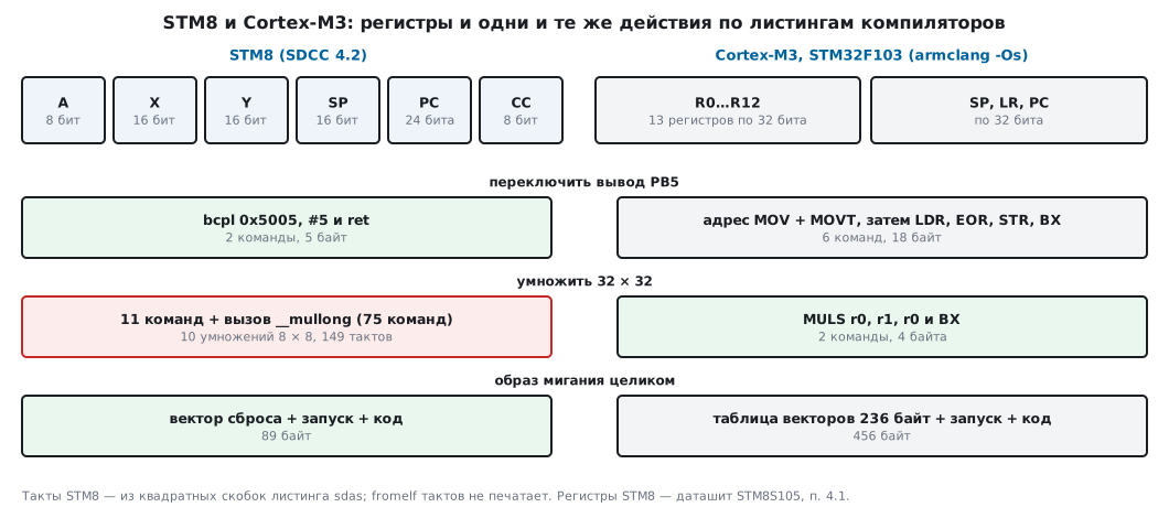
2в.2 The core: A, X, Y and a 24-bit program counter
According to the STM8S105 datasheet (section 4.1) the core has six registers:
- A — the eight-bit accumulator, arithmetic goes through it;
- X and Y — 16-bit index registers, also a pair for 16-bit numbers;
- SP — the stack pointer, 16 bits;
- PC — the program counter, 24 bits: an address space of 16 MB;
- CC — the flags, 8 bits, of which 7 are flags: 5 result flags and 2 interrupt mask bits.
80 instructions, 20 addressing modes, 8 × 8 multiplication and division 16 by 8 and 16 by 16 bits. For comparison: the Cortex-M3 has sixteen 32-bit registers (section 1.3), and multiplication on the F103, according to its datasheet, takes one cycle.
The SDCC listing shows how the compiler distributes numbers over these registers. A 16-bit sum: the first argument arrives in X, the second on the stack:
_add16:
  000000  72 FB 03  [2]  addw x, (0x03, sp)
  000003  90 85     [2]  popw y
  000005  5B 02     [2]  addw sp, #2
  000007  90 FC     [2]  jp (y)
The result stays in X. The last three instructions are the return: the function itself
removes its argument from the stack (it takes the return address into Y, moves SP
and jumps via Y). The figures in brackets are the instruction cycles, printed by the SDCC assembler.
A 32-bit sum lives in the Y:X pair — the low word in X, the high word in Y;
the carry between them is a conditional branch jrnc and the instruction incw y.
In SDCC for the STM8 an int is 2 bytes, a long 4, a pointer 2 bytes; this is
confirmed by _Static_assert in the experiment. As on the AVR (section 80): the expression
1000 * 60 already overflows in an int.
2в.3 Memory and the clock after reset
The STM8S105 memory map (datasheet, the memory map figure and table 7):
| Addresses | What is there |
|---|---|
| 0x0000–0x07FF | RAM, 2 KB; the top of the stack is the end of RAM |
| 0x4000–0x43FF | data EEPROM, 1 KB |
| 0x4800–0x487F | option bytes |
| 0x5000–0x57FF | ports and peripherals |
| 0x6000–0x67FF | boot ROM, 2 KB |
| 0x7F00… | core, SWIM, debug and interrupt registers |
| 0x8000–0x807F | 32 interrupt vectors |
| 0x8000–0xFFFF | program Flash, up to 32 KB |
The core registers are visible to the debugger at addresses: A at 0x7F00, SP at 0x7F08 and 0x7F09. After reset SP = 0x07FF — the top of RAM, so the startup code does not need to set up the stack. The EEPROM withstands 300 thousand write cycles (datasheet) — the F103 has no separate EEPROM, the pack description of the F103C8 has only Flash and RAM.
Other chips — from the files on disk:
| Flash | EEPROM | Source | |
|---|---|---|---|
| STM8S103 | 0x8000–0x9FFF, 8 KB | 0x4000–0x427F, 640 bytes | OpenOCD configuration |
| STM8L15x low density | 0x8000–0x9FFF, 8 KB | 0x1000–0x10FF, 256 bytes | stm8l15x_flash.h |
| STM8L15x medium density | 0x8000–0xFFFF, 32 KB | 0x1000–0x13FF, 1 KB | stm8l15x_flash.h |
| STM8L15x high density | 0x8000–0x17FFF, 64 KB | 0x1000–0x17FF, 2 KB | stm8l15x_flash.h |
On the larger STM8L the Flash goes beyond 0xFFFF — that is what the 24-bit program counter is for. A pointer in SDCC is still 2 bytes, though: data beyond 64 KB cannot be reached that way.
The clock after reset is the same on the STM8S and the STM8L — HSI 16 MHz divided by 8, that is 2 MHz — but the prescaler register is in different places:
| STM8S105 (datasheet) | STM8L15x (stm8l15x.h) |
|
|---|---|---|
CLK_CKDIVR |
0x50C6, 0x18 after reset | 0x50C0, 0x03 after reset |
Peripheral clocks CLK_PCKENR1 after reset |
0xFF — all enabled | 0x00 — all disabled |
| Clock bit for the ports | none | none |
| Slow internal oscillator | 128 kHz | 38 kHz |
On both the ports have no separate clock: there is nothing to enable, unlike the STM32 (section 8.4). The port addresses match — port B from 0x5005 on both.
2в.4 A register-level blink: SDCC versus armclang
ST's library for the STM8 does not suit SDCC: stm8l15x.h knows only the
Cosmic, Raisonance and IAR compilers, and on all others it stops the build
with the line #error "Unsupported Compiler!". So the addresses are our own, from the
STM8S105 datasheet (tables 8 and 9). The LED is on PB5:
#define PB_ODR     (*(volatile uint8_t *)0x5005)
#define PB_DDR     (*(volatile uint8_t *)0x5007)
#define PB_CR1     (*(volatile uint8_t *)0x5008)
#define PB_CR2     (*(volatile uint8_t *)0x5009)
#define CLK_CKDIVR (*(volatile uint8_t *)0x50C6)

#define LED (1u << 5)                   /* светодиод на PB5 */

void clock_16mhz(void)
{
    CLK_CKDIVR = 0x00;                  /* после сброса 0x18: HSI / 8 = 2 МГц */
}

void led_init(void)
{
    PB_DDR |= LED;                      /* выход */
    PB_CR1 |= LED;                      /* двухтактный */
    PB_CR2 &= (uint8_t)~LED;            /* медленный фронт */
}

void led_toggle(void)
{
    PB_ODR ^= LED;
}
The build is sdcc -mstm8 --std-c11 blink_stm8.c, with no warnings.
The .rst listing after linking:
_led_init:
  008029  72 1A 50 07  [1]  bset 0x5007, #5
  00802D  72 1A 50 08  [1]  bset 0x5008, #5
  008031  72 1B 50 09  [1]  bres 0x5009, #5
  008035  81           [4]  ret
_led_toggle:
  008036  90 1A 50 05  [1]  bcpl 0x5005, #5
  00803A  81           [4]  ret
Each |=, &= ~ and ^= became a single instruction on a bit right in memory:
bset, bres, bcpl. An interrupt cannot squeeze in between the read and the
write — it is one instruction. On the F103 the same needs BSRR or
bit-banding (sections 8.2 and 1.5). The same led_toggle from armclang:
led_toggle:
  f640400c  MOV r0,#0xc0c
  f2c40001  MOVT r0,#0x4001
  6801  LDR r1,[r0,#0]
  f0810120  EOR r1,r1,#0x20
  6001  STR r1,[r0,#0]
  4770  BX lr
Two 32-bit words go just to assembling the address 0x4001 0C0C
(GPIOB->ODR), then come the read, the "exclusive or", the write. The totals by
function and for the whole image:
| STM8S, SDCC | STM32F103, armclang -Os | |
|---|---|---|
led_init |
4 instructions, 13 bytes | 12 instructions, 36 bytes |
led_toggle |
2 instructions, 5 bytes | 6 instructions, 18 bytes |
| Blink image | 89 bytes | 456 bytes |
| Of which vectors | 4 bytes (reset only) | 236 bytes (59 words) |
The STM8 image: the reset vector and the jump to main — 7 bytes, zeroing and
copying data — 26, the jump to start — 3, the code — 53. The reset vector is 82 00 80 07:
the int instruction and a 24-bit address. SDCC writes only the vectors used into the table.
The F103 image is built with the Keil pack startup file and microlib; it contains
236 bytes of vector table. On the 8 KB STM8S103 a blink is 89 bytes,
on the 64 KB F103 it is 456: the difference is noticeable only on the smallest chips.
2в.5 Arithmetic from the listings
One source file arith.c is built by both compilers. A PC model
(stm8_2c.py) counts instructions and bytes from the listings, and for the STM8 also the sum of
cycles from the square brackets. fromelf has no cycles in its listing. Everything is counted together
with the function return; where the STM8 calls a library, its subroutine is built
from the SDCC sources and added:
| Operation | STM8: instructions | bytes | cycles | Cortex-M3: instructions | bytes |
|---|---|---|---|---|---|
| 16 + 16 bits | 4 | 9 | 8 | 3 | 6 |
| 32 + 32 bits | 7 | 15 | 14 | 2 | 4 |
| 8 × 8 bits | 6 | 9 | 11 | 2 | 4 |
8 × 8 with a cast to uint16_t |
32 | 51 | 56 | 2 | 4 |
| 16 × 16 bits | 25 | 42 | 50 | 3 | 6 |
| 32 × 32 bits | 86 | 142 | 149 | 2 | 4 |
- Addition. 16 bits is the native width of the X pair, one
addwinstruction. 32 bits — two additions and a carry. - 8 × 8 — one
mul x, ainstruction (4 cycles according to the listing). - 16 × 16 — a call to
__mulint: 19 instructions, threemul x, ainside. - 32 × 32 — a call to
__mullong: 75 instructions, 124 bytes, tenmul x, a, 149 cycles together with argument preparation. On the Cortex-M3 — a singleMULS. - A cast before multiplication.
(uint16_t)a * binstead ofa * bturns an 8 × 8 multiplication into 16 × 16: 6 instructions become 32 with a call to__mulint, although the result is the same.
Conclusion: on the STM8 keep data in 8 and 16 bits. Every uint32_t, and even
more so every float, is a library call.
2в.6 Debugging, programming and when the STM8 is appropriate
SWIM. One data wire instead of SWD's two: on the STM8S105 it is pin PD1.
According to the datasheet SWIM works in all chip modes and transfers up to 145 bytes
per millisecond; the debug module provides software breakpoints on any
instruction and two complex ones. The protocol is described in UM0470. The programmer is an ST-LINK:
in OpenOCD the STM8 connects only via SWIM (transport select swim),
and the networked ST-Link server does not support SWIM (OpenOCD manual).
For the STM8S103 OpenOCD has a ready file: 8 KB Flash, 64-byte write block.
Protection and the bootloader. Read protection is enabled with the ROP byte = 0xAA and
can be changed only via SWIM; any attempt to remove it erases the Flash and the EEPROM.
There is no BOOT0 pin as on the STM32 (section 4.9): after reset the boot ROM
looks at the bytes 0x487E, 0x487F and the reset vector and decides by itself whether to go
into the bootloader.
Environment. ST provides STVD and the STVP programmer; in the 2010 datasheet the free Cosmic and Raisonance are limited to 16 KB of code. SDCC has no limits, but no ST library: you describe the registers yourself, as in 2в.4. There is no CubeMX, HAL or LL for the STM8 — all of this exists only for the STM32.
When the STM8 is appropriate:
- a 5 V supply: the STM8S105 works from 2.95 to 5.5 V, the F103 from 2.0 to 3.6 V;
- you need real EEPROM rated for 300 thousand cycles, not writes to Flash;
- the task is small: polling buttons, relays, simple PWM, UART — 8 KB of Flash on the STM8S103 or 32 KB and 2 KB of RAM on the STM8S105 is enough, and the chip is the simplest;
- continuing an old product on the STM8: AN2945 directly offers migration in both directions.
When not:
- 32-bit arithmetic, filters, floating point — see 2в.5;
- you need USB, Ethernet, lots of RAM, an RTOS;
- a new project with no supply constraints: the STM32 has one environment, HAL and examples for the whole family, the STM8 has an old 2011 library and separate compilers.
There are no prices on disk, so there is no price comparison here: check it with the supplier at the time of ordering (section 2.5).
2в.7 Pitfalls
STM8S code does not start the clock on an STM8L. The port addresses are shared, but CLK_CKDIVR
is at 0x50C6 on the S and at 0x50C0 on the L. A write to the wrong address lands in a different
register.
A timer or the UART is silent on an STM8L. After reset CLK_PCKENR1 = 0x00 —
the peripheral clock is off, unlike on the STM8S (0xFF). The ports still work:
they have no separate clock.
The ST library does not build in SDCC. stm8l15x.h understands only
Cosmic, Raisonance and IAR: #error "Unsupported Compiler!". For SDCC —
your own register definitions from the datasheet.
An unnecessary type cast. (uint16_t)a * b for two uint8_t is a call to
__mulint instead of one mul instruction: 32 instructions instead of 6.
A 16-bit int. 1000 * 60 overflows, millisecond counters
in an int end at 32 767. Use uint32_t where it is really
needed, and remember that multiplying it is a library call.
Read protection erases everything. ROP cannot be removed without erasing the Flash and the EEPROM
— the data in the EEPROM will be lost too.
2в.8 Summary
- The STM8 is an eight-bit CISC core: A 8 bits, X and Y 16 each, PC 24 bits; according to AN2945 — 0.29 against 1.22 by Dhrystone and 9 cycles to an interrupt against 12 on the Cortex-M3.
- STM8S105: up to 16 MHz, 32 KB Flash, 2 KB RAM, 1 KB EEPROM, supply 2.95–5.5 V; 2 MHz after reset (HSI / 8), SP = 0x07FF.
- The ports on the STM8S and the STM8L are at the same addresses and have no clock; the clock prescaler and peripheral enabling differ.
- Blinking:
bset,bres,bcpl— one instruction per bit;led_toggleis 2 instructions and 5 bytes against 6 and 18 on the F103; the image is 89 bytes against 456. - Arithmetic: a 16-bit addition is 4 instructions, 32 × 32 is 86 instructions
and 149 cycles with
__mullongagainst a singleMULS. - Debugging is SWIM over one wire; the bootloader is selected by option bytes, not by a pin.
Full sources
blink_stm8.c — a register-level LED blink on the STM8S, built with SDCC.
/* Раздел 2в: мигание светодиодом на STM8S по регистрам, компилятор SDCC.
   Адреса — даташит STM8S105 (DocID14771): таблица 8 (порты) и таблица 9 (CLK). */
#include <stdint.h>

_Static_assert(sizeof(int) == 2 && sizeof(long) == 4 && sizeof(void *) == 2,
               "SDCC для STM8: int 2 байта, long 4, указатель 2");

#define PB_ODR     (*(volatile uint8_t *)0x5005)
#define PB_DDR     (*(volatile uint8_t *)0x5007)
#define PB_CR1     (*(volatile uint8_t *)0x5008)
#define PB_CR2     (*(volatile uint8_t *)0x5009)
#define CLK_CKDIVR (*(volatile uint8_t *)0x50C6)

#define LED (1u << 5)                   /* светодиод на PB5 */

void clock_16mhz(void)
{
    CLK_CKDIVR = 0x00;                  /* после сброса 0x18: HSI / 8 = 2 МГц */
}

void led_init(void)
{
    PB_DDR |= LED;                      /* выход */
    PB_CR1 |= LED;                      /* двухтактный */
    PB_CR2 &= (uint8_t)~LED;            /* медленный фронт */
}

void led_toggle(void)
{
    PB_ODR ^= LED;
}

static void delay(uint16_t n)
{
    while (n--) {
        __asm__("nop");
    }
}

void main(void)
{
    clock_16mhz();
    led_init();
    for (;;) {
        led_toggle();
        delay(50000u);
    }
}
blink_f103.c — the same blink on the STM32F103 via CMSIS, built with armclang.
/* Раздел 2в: то же мигание на STM32F103 по регистрам CMSIS, компилятор armclang. */
#include "stm32f10x.h"

#define LED (1u << 5)                   /* светодиод на PB5 */

void led_init(void)
{
    RCC->APB2ENR |= RCC_APB2ENR_IOPBEN;                     /* у STM32 порту нужен такт */
    GPIOB->CRL = (GPIOB->CRL & ~(0xFu << 20)) | (0x2u << 20); /* PB5: выход 2 МГц, двухтактный */
}

void led_toggle(void)
{
    GPIOB->ODR ^= LED;
}

static void delay(uint32_t n)
{
    while (n--) {
        __asm volatile("nop");
    }
}

int main(void)
{
    led_init();
    for (;;) {
        led_toggle();
        delay(50000u);
    }
}
Next: section 2г "Milandr K1986VE92: a domestic Cortex-M3 next to the STM32" — how a domestic chip on a familiar core differs from the F103 and what carries over without changes.