 Embedded HandbookApps
2д. The STM32U585CIU6 in a 48-pin package: what remains of the U585 and what to put it in
Section 2б compared the U585 with the F405 and took TrustZone apart, 10а covered its sleep modes.
There the U585 was the whole die: 2 MB of Flash, 786 KB of RAM, dozens of blocks.
Here it is its smallest package, UFQFPN48 (the letter C in the part number, 2б.1).
The die is the same, but fewer than half of the signals come out. The question of this section
is practical: which peripherals are really available on 48 pins, what to power it with,
how to start it at 160 MHz and what to build from all this.
Prerequisites: the datasheet DS13086 (rev. 8) and the reference manual RM0456 (rev. 4)
from the Keil pack STM32U5xx_DFP 2.2.1, the header stm32u585xx.h from the same place;
the device descriptions STM32U585CIUx.xml and STM32U585CIUxQ.xml from the
STM32CubeMX database; the board package B-U585I-IOT02A_BSP 1.1.0. The peripherals by pin
and the three products are computed by a script on a PC from the CubeMX files. The startup code is built with
armclang and run on a PC over "registers" in memory. QEMU does not model the U5,
and nothing was run on a board.
Terms used in the documentation
Term Meaning UFQFPN48 a leadless 7×7 mm package, 48 contacts along the sides Dedicated pinout supporting SMPS (Q) a pinout for the switching regulator — the letter Qat the end of the part numberLDO / SMPS step-down converter the linear regulator / the switching step-down regulator of the core VCAP, VDD11 the core pin for a capacitor: VCAPwith the LDO, twoVDD11with the SMPSVoltage scaling range 1…4 the core voltage range: 1 is the fastest, 4 the most economical EPOD booster the core supply booster: without it nothing above 55 MHz is allowed MSIS, MSIK the two outputs of the internal MSI oscillator: for the core and for the peripherals OCTOSPIM the pin switch of the two OCTOSPI controllers Linked-list item (GPDMA) a description of the next transfer kept in memory
2д.1 Two dies under one part number
The datasheet lists eight packages for the U585, from 48 to 169 pins. The 48-pin one has two variants, and CubeMX keeps them as separate files:
| STM32U585CIU6 | STM32U585CIU6Q | |
|---|---|---|
| Core regulator | LDO, pin VCAP |
SMPS and LDO, pins VLXSMPS, VDDSMPS, VSSSMPS, two VDD11 |
| I/O | 37 | 33 |
| Supply and reset | 11 | 15 |
| Wakeup pins | 17 | 15 |
| ADC inputs (pins) | 11 | 10 |
| TSC touch sensing channels | 5 | 4 |
The letter Q in the ordering scheme means "pinout for the SMPS". Pins 20…25 and 46 go to the inductor and the second
core supply; together with them PB2,
PB10, PB12 and PB9 disappear. The other 41 pins are the same.
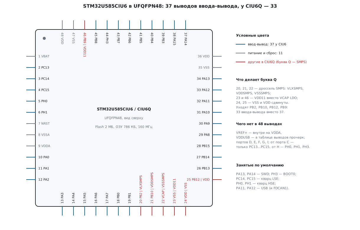
The figure also shows what is missing entirely on 48 pins: ports D, E, F, G and I;
of port C only PC13…PC15 remain, of port H PH0, PH1 and PH3
(which is also BOOT0). Five pins are almost always taken: PA13 and PA14 — SWD,
PH3 — boot selection, PC14 and PC15 — the watch crystal.
2д.2 What is brought out: peripherals by instance
The script pins2f.py takes from the CubeMX file the list of signals of each pin
and for each block looks for a complete set on different pins: TX
and RX for a UART, SCK, MISO, MOSI for SPI, SCL and SDA for I2C. A signal on a pin does not yet
mean that the block works: USART3 has its RX input only on PA5,
and if PA5 is taken, there is no USART3.
| Block | CIU6 (LDO) | CIU6Q (SMPS) |
|---|---|---|
| USART1, USART2, USART3, UART4, LPUART1 | all five | all five |
| SPI1, SPI2, SPI3 | all three | all three |
| I2C1…I2C4 | all four | all four |
| FDCAN1 | PA11/PA12 or PB8/PB9 |
only PA11/PA12 |
| USB OTG FS, UCPD1 | yes | yes |
| SAI1 | blocks A and B | blocks A and B |
| OCTOSPI | Quad: CLK, NCS, IO0…IO3; no IO4…IO7 | the same, CLK only on PA3 |
| SDMMC, DCMI, FMC, UART5 | no | no |
| TIM1…TIM5 | 4 channels each | TIM4 has 3 |
| TIM8 | only CH1N…CH4N | only CH1N…CH3N |
| TIM15, TIM16, TIM17 | 2, 1 and 1 channel | 2, 1 and 1 channel |
| LPTIM1…LPTIM3 / LPTIM4 | 2 channels each / no pins | the same |
| ADC inputs | 11: ADC1 — 11, ADC4 — 6 | 10 |
| DAC1 | PA4, PA5 |
PA4, PA5 |
The totals matched table 2 of the datasheet for STM32U585CI: 37/33
I/O, 17/15 wakeup pins, 11/10 ADC channels, SPI — 3,
I2C — 4, USART — 3, UART — 1, SAI — 1, SDMMC — 0. There are enough timers and
serial ports; on 48 pins what is lost is the parallel buses
(FMC, camera, SDMMC), the second SAI and the eight-line OCTOSPI.
2д.3 Power: SMPS or LDO, VBAT, VDDA and USB
The core. The U585 has two core regulators connected in parallel. The LDO
asks for a 4.7 µF capacitor on VCAP, the SMPS for a 2.2 µH inductor,
2.2 µF on each of the two VDD11 and 10 µF on VDDSMPS; the SMPS switching
frequency is 3 MHz with VDD above 1.9 V. After reset the LDO runs in range 4; switching to the SMPS
is done by the REGSEL bit in PWR_CR3 — in any range and on the fly.
The benefit is in the current. The core at 160 MHz from the PLL, peripherals off, 25 °C, typical values:
| Regulator | VDD | Current |
|---|---|---|
| LDO | 3.0 V | 13.50 mA |
| SMPS | 3.0 V | 7.15 mA |
| SMPS | 1.8 V | 10.50 mA |
From 3 V the switching regulator is almost twice as economical. The price is noise:
the RM states directly that the SMPS disturbs some applications, and then
they switch to the LDO. And in the package without Q the REGSEL bit is reserved
and must stay zero: the CIU6 has only the LDO.
VBAT (pin 1): 1.65…3.6 V, powers the RTC, the TAMP block, the 32 kHz clock oscillators, 2 KB of backup RAM and 32 backup registers. There are three tamper inputs on 48 pins, two of them active. Sleep modes and battery life are in 10а.
VDDA and VREF+. There is no separate VREF+ on 48 pins: it is connected to VDDA
inside the package, VREF− to VSSA. So the reference voltage of the ADC and DAC is
VDDA itself, and the built-in VREFBUF buffer is unavailable and must stay
off. The ADC accuracy here equals the accuracy of the analog supply.
USB. According to the datasheet VDDUSB is 3.0…3.6 V, but in the pinout table of both
48-pin packages there is a dash in its place. It cannot be supplied separately, so
for USB the whole supply of the chip is kept within these limits; the datasheet does not say this
directly, it is a conclusion from the tables. The USV bit in PWR_SVMCR is set all the same:
without it USB is isolated from its supply.
2д.4 External flash and GPDMA
On 48 pins the OCTOSPI has one port P1 and four data lines: IO0 — PB1,
IO1 — PB0, IO2 — PA7, IO3 — PA6, the clock — PA3 or PB10,
chip select — PA2 or PA4. This is enough for the Quad-SPI flash from section 41в,
but eight-line memory cannot be connected. Port P2 has only
its chip select brought out (PA0 or PA12). The datasheet says so: the two OCTOSPI
controllers in this package work only in multiplexed mode. They share the P1 lines
in turn, but each has its own chip select: this way two
chips are put on one bus.
For comparison — the B-U585I-IOT02A development board: on it the U585 is in a
169-ball package, the MX25LM51245G flash on OCTOSPI2 works on eight
lines at double data rate (the OPI and DTR modes in the board package),
the pins are ports F, H and I. An example from this board does not port to 48 pins.
Transfers between the flash, RAM and peripherals are handled by GPDMA1: 16 channels, each with its own data FIFO and a linked list — a chain of transfer descriptions in memory that the controller walks through by itself. The channels are not equal:
| Channels | Buffer | Addressing | What for |
|---|---|---|---|
| 0…11 | 8 bytes | linear | APB and AHB peripherals ↔ RAM |
| 12…15 | 32 bytes | two-dimensional | heavy AHB peripherals, external memory |
For OCTOSPI a channel from 12…15 is taken. GPDMA1 works on its own in Sleep, Stop 0 and Stop 1; in Stop 2 only LPDMA1 remains.
2д.5 A 160 MHz clock and a minimal start
After reset the core runs from MSIS at 4 MHz, the Flash has no wait states, the regulator is the LDO in range 4. The path to 160 MHz according to RM0456 (10.5.4) is:
- The PLL1 source is MSIS: 4 MHz at the PLL input fall into the 4…8 MHz window
(
PLL1RGE= 00). The booster prescaler is 1 (PLL1MBOOST= 0): the booster wants 4…16 MHz. - Range 1 (
VOS= 11) and theBOOSTENbooster; wait forVOSRDYandBOOSTRDY. Without a ready booster you must not go above 55 MHz. - Flash wait states: in range 1 — 4 cycles up to 160 MHz (3 — up to 128 MHz). RAM in range 1 needs no wait states up to 160 MHz.
- PLL1: ×80 → VCO 320 MHz (window 128…544), output R ÷2 → 160 MHz.
- Switch
SWto PLL1 and wait forSWS.
For the U59x/5Ax/5Fx/5Gx the RM additionally requires going above 80 MHz through the AHB prescaler; this does not apply to the U585.
/* Раздел 2д: минимальный старт STM32U585CIU6 / CIU6Q — стабилизатор, 160 МГц от MSIS, задержки Flash.
   Порядок — RM0456, 10.5.4 (повышение диапазона напряжения) и 7.3.3 (задержки Flash).
   USE_SMPS = 1 — только для корпуса с буквой Q (CIU6Q): в CIU6 бит REGSEL зарезервирован. */
#include "stm32u5xx.h"

#ifndef USE_SMPS
#define USE_SMPS 0
#endif

#define MSIS_HZ   4000000u          /* MSIS после сброса */
#define PLL_M     1u                /* 4 МГц на вход PLL1: окно 4…8 МГц, PLL1RGE = 00 */
#define PLL_N     80u               /* VCO 320 МГц: окно 128…544 МГц */
#define PLL_R     2u                /* PLL1R: только 1 или чётное */
#define REF_HZ    (MSIS_HZ / PLL_M)
#define VCO_HZ    (REF_HZ * PLL_N)
#define SYSCLK_HZ (VCO_HZ / PLL_R)
#define FLASH_WS  4u                /* диапазон 1: 4 такта ожидания — до 160 МГц */

_Static_assert(SYSCLK_HZ == 160000000u, "частота ядра");
_Static_assert(REF_HZ >= 4000000u && REF_HZ <= 8000000u, "вход PLL1 при PLL1RGE = 00");
_Static_assert(VCO_HZ >= 128000000u && VCO_HZ <= 544000000u, "VCO в диапазоне 1");
_Static_assert(SYSCLK_HZ > 128000000u && SYSCLK_HZ <= 160000000u, "4 такта Flash только для 128…160 МГц");
_Static_assert(RCC_PLL1CFGR_PLL1M_Msk == 0x00000F00u, "PLL1M — биты 11:8");
_Static_assert(RCC_PLL1CFGR_PLL1MBOOST_Msk == 0x0000F000u, "PLL1MBOOST — биты 15:12");

void clock_160mhz(void)
{
    RCC->AHB3ENR |= RCC_AHB3ENR_PWREN;                  /* такт блока PWR */
    (void)RCC->AHB3ENR;

#if USE_SMPS
    PWR->CR3 |= PWR_CR3_REGSEL;                         /* LDO -> SMPS */
    while (!(PWR->SVMSR & PWR_SVMSR_REGS)) {
    }
#endif

    /* 1. Источник PLL1 и делитель для бустера: 4 МГц / 1 */
    RCC->PLL1CFGR = RCC_PLL1CFGR_PLL1SRC_0              /* 01: MSIS */
                  | ((PLL_M - 1u) << RCC_PLL1CFGR_PLL1M_Pos);   /* PLL1MBOOST = 0, PLL1RGE = 00 */

    /* 2. Диапазон 1 и бустер: без BOOSTRDY выше 55 МГц нельзя */
    PWR->VOSR = PWR_VOSR_VOS_1 | PWR_VOSR_VOS_0 | PWR_VOSR_BOOSTEN;
    while ((PWR->VOSR & (PWR_VOSR_VOSRDY | PWR_VOSR_BOOSTRDY)) != (PWR_VOSR_VOSRDY | PWR_VOSR_BOOSTRDY)) {
    }

    /* 3. Задержки Flash до повышения частоты */
    FLASH->ACR = (FLASH->ACR & ~FLASH_ACR_LATENCY_Msk) | FLASH_WS | FLASH_ACR_PRFTEN;
    while ((FLASH->ACR & FLASH_ACR_LATENCY_Msk) != FLASH_WS) {
    }

    /* 4. PLL1: N и R пишутся минус один; выход R -> SYSCLK */
    RCC->PLL1DIVR = ((PLL_N - 1u) << RCC_PLL1DIVR_PLL1N_Pos)
                  | (1u << RCC_PLL1DIVR_PLL1P_Pos) | (1u << RCC_PLL1DIVR_PLL1Q_Pos)
                  | ((PLL_R - 1u) << RCC_PLL1DIVR_PLL1R_Pos);
    RCC->PLL1CFGR |= RCC_PLL1CFGR_PLL1REN;
    RCC->CR |= RCC_CR_PLL1ON;
    while (!(RCC->CR & RCC_CR_PLL1RDY)) {
    }

    /* 5. Переключение SYSCLK на PLL1 (11) */
    RCC->CFGR1 = (RCC->CFGR1 & ~RCC_CFGR1_SW_Msk) | (3u << RCC_CFGR1_SW_Pos);
    while ((RCC->CFGR1 & RCC_CFGR1_SWS_Msk) != (3u << RCC_CFGR1_SWS_Pos)) {
    }
}
armclang (-std=c11 -Os -Wall -Wextra -pedantic) builds both variants
without warnings: clock_160mhz is 140 bytes with the LDO and 152 bytes with the SMPS.
A copy with PLL_N = 90 (180 MHz) does not build: _Static_assert catches
the frequency already at compile time.
A check on a PC. model2f.c includes this file unchanged, but RCC,
PWR and FLASH are structures in PC memory, and a second thread plays the hardware:
it sets a ready flag only when the program has enabled the block, and records
the registers at that moment. In both variants PLL1 is enabled already with
LATENCY = 4 and range 1 with the booster, SW after PLL1RDY. The result:
PLL1CFGR = 0x00040001, PLL1DIVR = 0x0101024F, ACR = 0x00000104;
by the RM formula this is 4 MHz × 80 / 2 = 160 MHz.
2д.6 Three products on one chip
The script distributes the required signals over different pins by exhaustive search and counts what is left. Every project keeps SWD.
| Product | Chip | What is taken | Taken / free |
|---|---|---|---|
| Battery-powered sensor | CIU6Q | LSE, I2C3, LPUART1, wakeup pin PA0 |
9 / 24 |
| Crystal-less USB device | CIU6Q | LSE, USB, UCPD1 (CC1, CC2), USART1 | 10 / 23 |
| Node with external flash | CIU6 | HSE, OCTOSPI Quad, USB, FDCAN1, USART1 | 16 / 21 |
The sensor. CIU6Q — for the sake of the SMPS. I2C3 and LPUART1 were not chosen at random: according to the datasheet, in Stop 2 only ADC4, DAC1, LPTIM1, LPTIM3, LPTIM4, LPUART1, SPI3, I2C3, ADF1 and LPDMA1 work on their own. The sensor is read over I2C3, the data goes to the radio module over LPUART1, the core sleeps. 6 ADC inputs remain free, and SPI1 and SPI2 are free too.
USB without a crystal. No HSE is needed: MSIK in range 0 (about 48 MHz,
MSIKRANGE = 0000 with MSIRGSEL = 1) is trimmed against the watch crystal —
MSIPLLSEL = 0, then MSIPLLEN = 1, and only after LSERDY. USB takes
its clock through ICLKSEL = 11. Accuracy is better than ±0.25 % according to the datasheet; the mechanism
and the USB tolerance are covered in 20а. The PH0 and PH1 pins are freed;
on the 23 free pins there is still room for OCTOSPI Quad, SPI1, SPI3,
all four I2C and 10 ADC inputs.
The node with flash. The CIU6 is needed here: FDCAN1 and USB fit together only
in it — FDCAN1 goes to PB8/PB9. In the CIU6Q FDCAN1 has its transmitter
only on PA12, and that is USB D+, so the search finds no solution. The HSE crystal
is needed for CAN. OCTOSPI takes PA2, PA3, PA6, PA7, PB0, PB1,
so 5 ADC inputs remain.
2д.7 Pitfalls
A board for the CIU6, but a CIU6Q is soldered on. The part numbers differ by one letter,
but pins 20…25 and 46 differ more. A CIU6 board supplies VDD to pin 24, while on the CIU6Q
that is VSS; pin 25 is expected to be PB12, but there is a supply there. The letter Q is checked
in the bill of materials and at incoming inspection.
REGSEL on the CIU6. In the package without the SMPS the bit is reserved. Code
with USE_SMPS = 1 for such a chip is a mistake; one project
for both variants can be kept only through this build flag.
A failure after leaving Stop. BOOSTEN is cleared in all Stop
modes, and after exit the range is 4 again. Raising the clock to 160 MHz is repeated
in full, starting with the range and the booster.
USB and CAN on the same pins. In the CIU6Q FDCAN1_TX exists only on PA12.
The choice between the CIU6 and the CIU6Q is made before layout, by a search as in 2д.6.
The comment on a mask lies. In stm32u585xx.h, for 226 of the 7306 definitions
of the form (0x…UL << …_Pos) the number in the comment is not equal to the mask. For PLL1M
and PLL1MBOOST it says 0x000003F0, while in fact they are 0x00000F00
and 0x0000F000. Trust the name, not the comment; in the code above this is checked by
_Static_assert.
USB lost its accuracy. If the watch crystal stops, MSI leaves the trimming mode and drifts. On all U5 except the U575/585 revision X this event is routed to an EXTI line; on revision X it cannot be caught by an interrupt.
VREFBUF was enabled. On 48 pins VREF+ is connected to VDDA, the buffer
must stay off.
2д.8 Summary
- STM32U585CIU6 — 48 pins, 37 of them I/O; the CIU6Q with the SMPS has 33:
PB2,PB9,PB10,PB12go away, pins 20…25 and 46 change. - On 48 pins there are all the USARTs, SPIs, I2Cs, USB, UCPD, FDCAN1 and SAI1; there is no SDMMC, FMC, camera or eight-line OCTOSPI — only Quad on P1.
- SMPS: a 2.2 µH inductor, 2 × 2.2 µF on
VDD11; at 160 MHz and 3 V — 7.15 mA against 13.50 mA with the LDO. VREF+is connected toVDDAinside,VREFBUFis unavailable;VDDUSBhas no pin of its own.- GPDMA1: 16 channels, 12…15 have a 32-byte buffer and two-dimensional addressing — they are given to external memory.
- 160 MHz from MSIS: ×80 ÷2, range 1 with the booster, 4 Flash cycles; the code is 140 bytes (LDO) and 152 bytes (SMPS).
- The sensor takes 9 pins of 33, crystal-less USB 10 of 33, the node with flash, USB and CAN 16 of 37 and only on the CIU6.
Next: section 2е "TrustZone in practice: SAU, GTZC, the call gateway and two projects on the STM32U585" — how the U585 is partitioned with TrustZone enabled and how to build the secure and non-secure projects.