 Embedded HandbookApps
11. Memory, linking, loading
Quite a lot happens between applying power and the first line of main.
While everything works, you do not need to know this — but only until the first stack
overflow or "the variable changed by itself". This section is about where everything lies
and who put it there.
Terms used in the documentation
Term Meaning linker script the file that tells the linker where to place everything section a named part of the program image startup code the code that runs before mainstack pointer the register that points to the top of the stack heap the area for mallocvector table the array of handler addresses option bytes the bytes that configure the chip itself read protection protection of Flash against reading boot mode where the chip starts from stack overflow the stack growing beyond its area log-structured storage storage as a log of records erased state the erased state: all bits are ones power-loss safe robust against power loss
11.1 Where everything lies
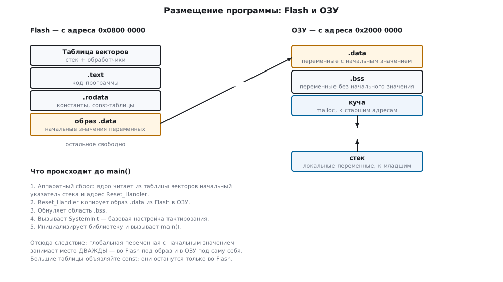
The build lays the program out into sections, and each has its own place:
| Section | What is in it | Where it lives |
|---|---|---|
.text |
code | Flash |
.rodata |
constants, const tables, string literals |
Flash |
.data |
variables with an initial value | RAM, image in Flash |
.bss |
variables without an initial value | RAM |
| stack | local variables, return addresses | RAM, from the top edge |
| heap | malloc |
RAM, after .bss |
A consequence that saves memory. A global variable
with an initial value takes space twice: in Flash for the image of the initial
value and in RAM for itself. A large table declared without const
eats kilobytes of scarce RAM:
uint8_t  font[2048] = { /* ... */ };   /* 2 КБ Flash + 2 КБ ОЗУ */
const uint8_t font[2048] = { /* ... */ };  /* только 2 КБ Flash */
On a chip with 20 KB of RAM the difference is decisive.
A variable without initialisation goes into .bss and costs only space in RAM:
it has no image in Flash, because the start-up code simply fills
this area with zeros.
11.2 What happens before main
- Hardware reset. The core reads the first two words from the vector table:
the initial value of the stack pointer and the address of
Reset_Handler. SystemInit. Basic clock configuration and, if needed, relocation of the vector table. In the Keil start-up file this is the first call ofReset_Handler, even before the library__main.- Copying
.data. The start-up code moves the image of the initial values from Flash to RAM. - Zeroing
.bss. The area is filled with zeros — this is why uninitialised global variables are guaranteed to be zero, while local ones are not. In Keil both steps are done by__main. - Library initialisation and the call to
main.
⚠️ Global variables are not ready yet in
SystemInit. In KeilSystemInitis called before__main: whatever is written to a global variable will later be overwritten by the.dataimage or the.bsszeros. In ST start-up files for GCC the order depends on the family: on F0, F3 and F4SystemInitcomes after the copying, on G0, G4, L4, H7 and U5 before it. It is safer not to touch global variables inSystemInitat all.
All this lies in the start-up file, which is added to the project together with the device pack. It is usually not touched, but it is useful to know it is there: it is exactly where the weak stubs of the interrupt handlers are declared, which are replaced by your functions (section 7).
⚠️ Local variables are not zeroed. Global ones are, by the start-up code. A local variable gets whatever was left at that place on the stack by previous calls. The classic mistake is to count on a zero initial value of a local counter.
11.3 The linker script
The file that says where to put which section. It is usually generated by the environment, and it rarely has to be edited — but it is useful to understand it.
There are two key parts. The description of the memory regions:
MEMORY
{
  FLASH (rx)  : ORIGIN = 0x08000000, LENGTH = 64K
  RAM   (rwx) : ORIGIN = 0x20000000, LENGTH = 20K
}
And the placement of sections into these regions — where .text goes into FLASH,
and .data is declared in RAM, but with a reference to an image in FLASH.
When the script has to be edited:
- to place a buffer in a particular region (for example, to move data out of CCM, which is inaccessible to DMA — section 9);
- to leave room at the end of Flash for your own settings storage, so that the linker does not fill it with code;
- to shift the start of the program if your own bootloader stands in front of it;
- to set the stack and heap sizes.
A variable can be placed in a specific section with an attribute:
uint8_t dma_buffer[512] __attribute__((section(".sram2")));
The attribute works only together with the script: in MEMORY you create an SRAM2 region
(on F407 — 16 KB from 0x2001C000, and RAM is shortened to 112 KB), in SECTIONS —
.sram2 (NOLOAD) : { *(.sram2) } > SRAM2. Without this GNU ld will put the section
wherever it ends up. The start-up code does not zero such a section — the initial value
is set in the program.
11.4 The stack and the heap
Both areas live in the same RAM and grow towards each other: the stack from the top
boundary towards lower addresses, the heap from the end of .bss towards higher ones.
Between them is free space, and if they meet, the program corrupts
its own data.
How much stack is needed. Every function call puts the return address, registers and local variables there. An interrupt adds its own frame on top. Deep recursion or a large local array eat the stack instantly:
void parse(void)
{
    uint8_t buffer[4096];   /* 4 КБ на стеке при 20 КБ ОЗУ — почти наверняка крах */
}
Such buffers are made static or global.
⚠️ A stack overflow gives no error — on Cortex-M3/M4 without an MPU. The stack simply runs over
.bssand corrupts variables. It shows up as "data changes by itself", and at a place in no way connected with the real cause. One of the most elusive classes of faults — debugging techniques are in section 35. An overflow can be caught with an MPU guard (section 11а), and on Cortex-M33 with the stack limit registersMSPLIMandPSPLIM.
About malloc on a microcontroller. Dynamic memory is rarely appropriate here:
the heap fragments, and there is usually nowhere to handle an allocation failure.
The standard approach is pre-allocated static buffers of fixed
size. If dynamics are needed after all, it is better to take them from an RTOS (section 25),
where at least the behaviour on shortage is predictable.
11.5 🔧 Writing to the internal Flash
A microcontroller can write to its own Flash — this is how settings, calibrations and operating hour counters are stored.
The order: unlock, erase the page, write, lock.
static void flash_unlock(void)
{
    if (FLASH->CR & FLASH_CR_LOCK) {
        FLASH->KEYR = FLASH_KEY1;      /* 0x4567 0123 */
        FLASH->KEYR = FLASH_KEY2;      /* 0xCDEF 89AB */
    }
}

uint8_t flash_erase_page(uint32_t addr)
{
    flash_unlock();
    flash_wait();
    FLASH->SR = FLASH_SR_PGERR | FLASH_SR_WRPRTERR | FLASH_SR_EOP;  /* флаги сбрасываются единицей */

    FLASH->CR |= FLASH_CR_PER;         /* режим стирания страницы */
    FLASH->AR = addr;                  /* любой адрес внутри страницы */
    FLASH->CR |= FLASH_CR_STRT;        /* пуск */
    flash_wait();
    FLASH->CR &= ~FLASH_CR_PER;        /* обязательно снять режим */

    flash_lock();
    return (FLASH->SR & (FLASH_SR_PGERR | FLASH_SR_WRPRTERR)) ? 1u : 0u;
}

uint8_t flash_write(uint32_t addr, const uint16_t *data, uint32_t count)
{
    if (addr & 1u) {
        return 1u;                     /* адрес обязан быть чётным */
    }

    flash_unlock();
    flash_wait();
    FLASH->SR = FLASH_SR_PGERR | FLASH_SR_WRPRTERR | FLASH_SR_EOP;
    FLASH->CR |= FLASH_CR_PG;

    for (uint32_t i = 0; i < count; i++) {
        *(volatile uint16_t *)(addr + i * 2u) = data[i];
        flash_wait();
        if (FLASH->SR & FLASH_SR_PGERR) {
            FLASH->CR &= ~FLASH_CR_PG;
            flash_lock();
            return 1u;                 /* писали в нестёртую память */
        }
    }

    FLASH->CR &= ~FLASH_CR_PG;
    flash_lock();
    return 0u;
}
⚠️ On F1 you can write only in half-words. Not in bytes and not in words — exactly 16 bits at a time, at even addresses. A byte or word write with
PGset is a bus error and a HardFault. ThePGERRflag means something else: the cell at the address is not erased. On F4 the width is selected by thePSIZEfield, but it depends on the supply voltage: 32 bits are not always available.⚠️ The unlock keys go strictly in order. If you write a wrong one, the programming block locks until reset, and further attempts are useless.
Reading requires no ceremony: Flash is mapped into memory, read it as an ordinary variable at an address.
The difference between families: on F1 the erase unit is a page of 1 KB (2 KB on the senior ones), on F4 a sector, and of different sizes: the first four are 16 KB, then one of 64 KB, then 128 KB each. Setting aside "the last page for settings" on F4 means sacrificing 128 KB at once.
How to store settings so that the page does not wear out and a power loss spoils nothing — in 11.8.
11.6 Option bytes and protection
A separate small area that configures the behaviour of the chip itself:
| Parameter | What it does |
|---|---|
| RDP | protection of Flash against reading through the debugger |
| WRP | write protection of individual pages |
nRST_STOP, nRST_STDBY |
whether to reset the chip on entering sleep modes |
WDG_SW |
hardware or software watchdog |
⚠️ Read protection is removed only together with erasing the whole Flash. This is not a side effect but the intent: otherwise the protection would make no sense. By enabling it during debugging you will not "lock the board forever" — but you will start every reflash with a full erase. The second protection level on some families, however, is irreversible: the debug interface is disabled for good.
The protection level is set by the value of the RDP byte:
| Level | F1 | F4 | What it means |
|---|---|---|---|
| 0 | 0xA5 |
0xAA |
no protection |
| 1 | any other | any except 0xAA and 0xCC |
the debugger cannot read Flash; removal only with erasing the whole Flash |
| 2 | none | 0xCC |
forever: debugging and booting from system memory are disabled, the option bytes can no longer be changed |
On both series "no protection" is one special value, and all the others protect.
That is why erased option bytes (0xFF) give a protected chip, not an open one.
11.7 How the chip chooses where to start from
This was already covered in section 4 with regard to flashing; here it is from the memory side:
| BOOT1 | BOOT0 | Where it starts from |
|---|---|---|
| × | 0 | from Flash — normal operation |
| 0 | 1 | from system memory — the factory bootloader |
| 1 | 1 | from RAM |
In a normal boot Flash is aliased at address 0x0000 0000, so
the vector table ends up where the core expects it. When starting from system
memory, the factory bootloader is mapped to address zero.
Your own bootloader is built on the same mechanism: the program occupies the start of Flash, checks a condition (a button is pressed, a command has arrived), if necessary receives new firmware and writes it further on, and then passes control to the main application. The main application then has to relocate the vector table:
SCB->VTOR = 0x08008000u; /* если приложение начинается с 32 КБ */
On F1 SystemInit itself writes SCB->VTOR = FLASH_BASE | VECT_TAB_OFFSET —
instead of the line you can set VECT_TAB_OFFSET = 0x8000 there. And the jump
from the bootloader to the application is not one line: disable interrupts,
stop SysTick, load MSP from the first word of the application's table
and jump to the address from the second (section 48).
The forgotten line gives the most confusing effect: the program works until the first interrupt comes — and then goes into the bootloader's handler.
11.8 🔧 Settings in Flash: a log of records
Writing as in 11.5 works, but if you erase the page and write the settings anew on every save, three troubles arise.
- Wear. The guaranteed endurance of a page on F1 and F4 is 10 000 erases. A "save" button pressed 100 times a day will use it up in 100 days.
- Power loss. Between the erase and the write the settings exist nowhere: if the power goes off at that moment, after power-up there is nothing.
- New firmware. You added a field to the structure — the old bytes are read with the new layout and turn into garbage.
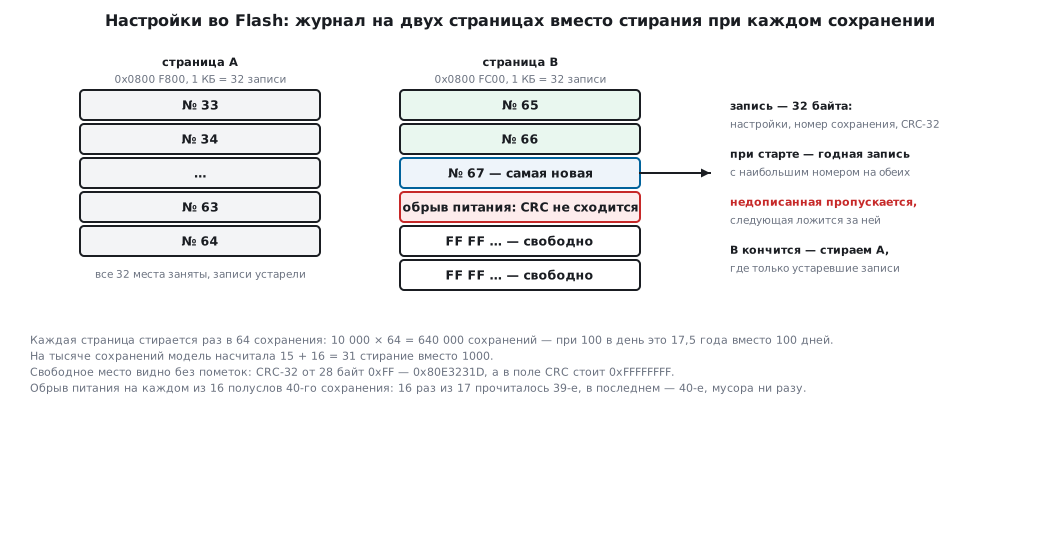
The solution is a log on two pages. A record is 32 bytes: the settings, a save number and a CRC-32. New records go one after another into free space; a page is erased only when space has run out — and not the current one but the other, where only outdated records lie. At start-up the valid record with the highest number is taken.
typedef struct {
    uint16_t version;                   /* раскладка структуры */
    uint16_t brightness;
    int16_t  offset_mv;
    uint16_t flags;
    uint32_t baud;
    char     name[12];
} cfg_t;

typedef struct {
    cfg_t    cfg;
    uint32_t seq;                       /* номер сохранения */
    uint32_t crc;                       /* CRC-32 от cfg и seq */
} rec_t;

/* годная запись с наибольшим номером на обеих страницах */
static const rec_t *newest(uint32_t *page_of)
{
    const rec_t *best = NULL;
    for (uint32_t p = CFG_BASE; p < CFG_BASE + 2u * PAGE; p += PAGE)
        for (uint32_t i = 0; i < SLOTS; i++) {
            const rec_t *r = slot(p, i);
            if (r->crc == crc32(r, offsetof(rec_t, crc)) && (best == NULL || r->seq > best->seq)) {
                best = r;
                *page_of = p;
            }
        }
    return best;
}

int cfg_save(const cfg_t *in)
{
    uint32_t page = CFG_BASE, i;
    const rec_t *old = newest(&page);
    rec_t rec;
    uint16_t buf[sizeof(rec_t) / 2];

    for (i = 0; i < SLOTS && !is_free(slot(page, i)); i++) { }
    if (i == SLOTS) {                   /* страница кончилась: стираем другую — */
        page = (page == CFG_BASE) ? CFG_BASE + PAGE : CFG_BASE;
        if (flash_erase_page(page))     /* там только устаревшие записи */
            return 1;
        i = 0;
    }
    memcpy(&rec.cfg, in, sizeof rec.cfg);
    rec.seq = old ? old->seq + 1u : 1u;
    rec.crc = crc32(&rec, offsetof(rec_t, crc));
    memcpy(buf, &rec, sizeof buf);      /* запись — полусловами */
    return flash_write(page + i * sizeof(rec_t), buf, sizeof buf / 2u);
}

/* при старте: сохранённое, а если его нет или раскладка другая — умолчания */
void cfg_get(cfg_t *out)
{
    if (!cfg_load(out) || out->version != CFG_VERSION)
        *out = cfg_defaults;
}
The log occupies the last two pages of F103C8 — 0x0800 F800 and 0x0800 FC00;
erasing and half-word writing are the functions from 11.5. crc32 is an ordinary bitwise
CRC-32 with the polynomial 0xEDB88320, the same as in archivers.
Wear. A page holds 32 records, the pages alternate, and each is erased once every 64 saves: 10 000 × 64 = 640 000 saves. At 100 saves a day this is 6400 days, 17.5 years instead of 100 days. The model counted 15 + 16 = 31 erases instead of 1000 over a thousand saves.
Power loss. Erased Flash is all ones, so free space can be seen without separate marks. It will not pass for a valid record: the CRC-32 of 28 bytes of 0xFF is 0x80E3231D, while the CRC field holds 0xFFFFFFFF. A half-written record is neither free nor valid — it is skipped, and the next one goes after it.
The model cut the power at 17 points of the 40th save: before the first of the 16 half-words and after each of them. 16 times out of 17 the 39th save was read after power-up, and in the last case, when all 16 half-words had been written, the 40th; there was never any garbage, and the next save went through every time. A cut in the middle of an erase is not dangerous either: the page being erased is the one without the latest record, which lies on the other one — after such a cut the model read the 64th save.
Version. The version field distinguishes a record of the previous firmware with a different
layout: cfg_get returns the defaults instead of it. In the model a saved
brightness of 77 with version 0 gave the default 500 at start-up.
On F4 it is the same, only a sector is erased. For the log you set aside either two 16 KB sectors right after the vector table — 16 384 / 32 = 512 records in each, but then the program image skips them in the linker script (11.3), — or the last two 128 KB sectors: simple, but expensive.
⚠️ While an erase is in progress, code from Flash is not executed. F1 has one bank, and instruction fetches wait for the page erase to finish — that is tens of milliseconds. Interrupts are delayed all that time. Save when it does no harm, or keep the urgent handler in RAM. On F407 erasing takes longer: a 16 KB sector — 0.25 s typically and up to 0.5 s, a 128 KB sector — 1 s and up to 2 s (when writing by word; by byte it is even longer). The watchdog timeout (12.2) is chosen with a margin for erasing.
⚠️ F1 writes and erases Flash only with HSI enabled. Whoever switched off the internal oscillator to save power after moving to the crystal will get Flash that does not write.
⚠️ A block larger than a page. On F103C8 a page is 1 KB. A structure written as a 2 KB block runs onto the neighbouring page, which nobody erased, and the write breaks off with a programming error in the middle.
11.9 F0 and G0: half-words on F0, double words on G0
F0 writes to Flash like F1: only in half-words, a page is erased
at any address inside it through FLASH->AR, the unlock keys are the same.
Recipe 11.5 ports without changes; only the page size differs —
on F072 2 KB (on F03x–F05x 1 KB), 64 pages per 128 KB:
    FLASH->CR |= FLASH_CR_PER;
    FLASH->AR = addr;                           /* любой адрес внутри страницы */
    FLASH->CR |= FLASH_CR_STRT;
*(volatile uint16_t *)(addr + i * 2u) = data[i]; /* полусловами, как у F1 */
G0 has a different controller, shared with L4, G4 and the H7 family: the registers
are shifted (KEYR at 0x08, CR at 0x14), there is no AR register — a page is
erased by number in the PNB field of the CR register, and writing is done in double
words: the address is a multiple of 8, two 32-bit words in a row. A byte or a half-word
the controller rejects with the size error SIZERR, and two words not from the same
double word with the alignment error PGAERR. The keys are not declared in the chip
header — they are in HAL, with the same values 0x45670123 and 0xCDEF89AB.
Busy is not BSY but BSY1 and CFGBSY; the errors are SIZERR, PGAERR,
PGSERR, PROGERR, WRPERR. Before a new operation they are cleared by writing
ones to FLASH->SR: with an uncleared flag the controller will set PGSERR,
and the write will not start. F1/F0 code does not build on G0: no member named 'AR' in
'FLASH_TypeDef'.
    FLASH->CR = (FLASH->CR & ~FLASH_CR_PNB) | (page << FLASH_CR_PNB_Pos) | FLASH_CR_PER;   /* номер, не адрес */
    FLASH->CR |= FLASH_CR_STRT;
        *(volatile uint32_t *)(addr + i * 8u) = (uint32_t)data[i];
        __ISB();
        *(volatile uint32_t *)(addr + i * 8u + 4u) = (uint32_t)(data[i] >> 32);
        flash_wait();
For the settings log from 11.8 this means: on G0 writing goes in portions of 8 bytes, and the log record size should be made a multiple of eight, not two. The page on G071 is the same 2 KB, 64 pages per 128 KB.
11.10 Pitfalls
A local counter does not start from zero. Local variables are not zeroed by the start-up code (11.2).
Variables change "by themselves". The stack overflowed and ran over .bss; there is no error (11.4).
HardFault when writing to F1 Flash. You wrote a byte or a word, but only half-words at even addresses are allowed (11.5).
A write to F1 Flash raises PGERR. You wrote to a cell that was not erased: erase the page before writing (11.5).
The programming block locked until reset. The unlock keys were written in the wrong order (11.5).
Read protection can be removed only by erasing the whole Flash, and the second protection level on some families is irreversible (11.6).
Interrupts are late by tens of milliseconds when saving settings. While an erase is in progress, code from Flash is not executed (11.8).
F1 Flash does not write after moving to the crystal. Writing and erasing require HSI to be enabled (11.8).
A write breaks off in the middle of a block. A block larger than a page (on F103C8 — 1 KB) ran onto the unerased neighbouring one (11.8).
11.11 Summary
- A variable with an initial value takes space twice: in Flash for the image
and in RAM for itself.
conston large tables keeps them only in Flash. - Global variables are zeroed by the start-up code, local ones are not.
- The stack and the heap grow towards each other; a stack overflow gives no error but quietly corrupts neighbouring data.
- Make large buffers static, not local.
- On F1 Flash is programmed only in half-words at even addresses.
- The Flash unlock keys go strictly in order; a mistake locks the block until reset.
- The erase unit: on F1 a 1 KB page, on F4 a sector from 16 to 128 KB.
- Read protection is removed only by a full erase; the second level
on some families is irreversible. No protection is only
RDP= 0xA5 (F1) or 0xAA (F4); on F4 the value 0xCC disables debugging forever. - Settings are stored as a log on two pages: records in a row, only the page with outdated records is erased, a record has a number and a CRC. Endurance grows 64 times, a power loss spoils nothing, the version field protects against a change of layout.
- An application behind a bootloader must relocate
SCB->VTOR, otherwise interrupts will go to someone else's handlers.
Full sources
flash_f0.c — writing to STM32F072 Flash in half-words.
/* Раздел 11.9: запись во Flash STM32F072 — как у F1: полусловами, стирание по адресу. */
#include <stddef.h>
#include "stm32f0xx.h"

_Static_assert(offsetof(FLASH_TypeDef, KEYR) == 0x04u && offsetof(FLASH_TypeDef, AR) == 0x14u, "KEYR и AR как у F1");
_Static_assert(FLASH_BANK1_END == 0x0801FFFFu, "128 КБ Flash у F072");
#define PAGE_SIZE 2048u                         /* у F072 страница 2 КБ (у F03x/F04x/F05x — 1 КБ) */
_Static_assert((FLASH_BANK1_END + 1u - FLASH_BASE) / PAGE_SIZE == 64u, "64 страницы");

static void flash_unlock(void)
{
    if (FLASH->CR & FLASH_CR_LOCK) {
        FLASH->KEYR = FLASH_KEY1;
        FLASH->KEYR = FLASH_KEY2;
    }
}

static void flash_wait(void)
{
    while (FLASH->SR & FLASH_SR_BSY) {
    }
    if (FLASH->SR & FLASH_SR_EOP) {
        FLASH->SR = FLASH_SR_EOP;
    }
}

uint8_t flash_erase_page_f0(uint32_t addr)
{
    flash_unlock();
    flash_wait();
    FLASH->CR |= FLASH_CR_PER;
    FLASH->AR = addr;                           /* любой адрес внутри страницы */
    FLASH->CR |= FLASH_CR_STRT;
    flash_wait();
    FLASH->CR &= ~FLASH_CR_PER;
    FLASH->CR |= FLASH_CR_LOCK;
    return (FLASH->SR & (FLASH_SR_PGERR | FLASH_SR_WRPRTERR)) ? 1u : 0u;
}

uint8_t flash_write_f0(uint32_t addr, const uint16_t *data, uint32_t count)
{
    if (addr & 1u) {
        return 1u;
    }
    flash_unlock();
    flash_wait();
    FLASH->CR |= FLASH_CR_PG;
    for (uint32_t i = 0; i < count; i++) {
        *(volatile uint16_t *)(addr + i * 2u) = data[i];   /* полусловами, как у F1 */
        flash_wait();
    }
    FLASH->CR &= ~FLASH_CR_PG;
    FLASH->CR |= FLASH_CR_LOCK;
    return (FLASH->SR & (FLASH_SR_PGERR | FLASH_SR_WRPRTERR)) ? 1u : 0u;
}
flash_g0.c — writing to STM32G071 Flash in double words.
/* Раздел 11.9: запись во Flash STM32G071 — двойными словами, стирание по номеру страницы. */
#include <stddef.h>
#include "stm32g0xx.h"

_Static_assert(offsetof(FLASH_TypeDef, KEYR) == 0x08u && offsetof(FLASH_TypeDef, CR) == 0x14u, "KEYR на 0x08, CR на 0x14");
#define PAGE_SIZE 2048u                         /* страница 2 КБ */
#define FLASH_KB  128u                          /* G071xB */
_Static_assert(FLASH_KB * 1024u / PAGE_SIZE == 64u, "64 страницы");
_Static_assert(FLASH_CR_PNB_Pos == 3u, "номер страницы — поле PNB в CR");
/* ключи в заголовке камня G0 не объявлены — они в HAL (stm32g0xx_hal_flash.h); значения те же, что у F1 и F0 */
#define FLASH_KEY1 0x45670123u
#define FLASH_KEY2 0xCDEF89ABu

static void flash_unlock(void)
{
    if (FLASH->CR & FLASH_CR_LOCK) {
        FLASH->KEYR = FLASH_KEY1;
        FLASH->KEYR = FLASH_KEY2;
    }
}

static void flash_wait(void)
{
    while (FLASH->SR & (FLASH_SR_BSY1 | FLASH_SR_CFGBSY)) {   /* BSY1 и CFGBSY, не BSY */
    }
    if (FLASH->SR & FLASH_SR_EOP) {
        FLASH->SR = FLASH_SR_EOP;
    }
}

uint8_t flash_erase_page_g0(uint32_t page)
{
    flash_unlock();
    flash_wait();
    FLASH->CR = (FLASH->CR & ~FLASH_CR_PNB) | (page << FLASH_CR_PNB_Pos) | FLASH_CR_PER;   /* номер, не адрес */
    FLASH->CR |= FLASH_CR_STRT;
    flash_wait();
    FLASH->CR &= ~FLASH_CR_PER;
    FLASH->CR |= FLASH_CR_LOCK;
    return (FLASH->SR & (FLASH_SR_PGAERR | FLASH_SR_PGSERR | FLASH_SR_WRPERR)) ? 1u : 0u;
}

/* Запись двойными словами: адрес кратен 8, каждая запись — два слова подряд. */
uint8_t flash_write_g0(uint32_t addr, const uint64_t *data, uint32_t count)
{
    if (addr & 7u) {
        return 1u;
    }
    flash_unlock();
    flash_wait();
    FLASH->CR |= FLASH_CR_PG;
    for (uint32_t i = 0; i < count; i++) {
        *(volatile uint32_t *)(addr + i * 8u) = (uint32_t)data[i];
        __ISB();
        *(volatile uint32_t *)(addr + i * 8u + 4u) = (uint32_t)(data[i] >> 32);
        flash_wait();
    }
    FLASH->CR &= ~FLASH_CR_PG;
    FLASH->CR |= FLASH_CR_LOCK;
    return (FLASH->SR & (FLASH_SR_PGAERR | FLASH_SR_PGSERR | FLASH_SR_WRPERR)) ? 1u : 0u;
}
Next: section 11а "MPU: protecting memory from your own mistakes".