 Embedded HandbookApps
10б. LPBAM on STM32U5: peripherals work in Stop 2 while the core sleeps
Section 10а ended with a conclusion: the battery is eaten not by sleep but by wake-ups. On L4 LPUART1 and LPTIM1 live in Stop 2, but every received byte and every measurement still wakes the core. U5 takes the next step: a timer starts the ADC, the ADC hands a sample to the transfer controller, which puts it into memory — and all this in Stop 2, without a single program instruction. ST calls this LPBAM. Here — what it is built from, what it looks like in the registers and when it pays off.
Prerequisites: the reference manual RM0456 (rev. 4) — sections 10.7.2, 11.4.24,
chapters 18 (LPDMA), 34 (ADC4) and 58 (LPTIM); the datasheet DS13086 (rev. 8);
the header stm32u585xx.h and the HAL 1.3.0 driver from the STM32U5xx_DFP 2.2.1 pack;
the STM32CubeMX database. The firmware was built with arm-none-eabi-gcc 12.2.1 and armclang
for Cortex-M33. The node table from the object file is executed by a model of
the channel on a PC. QEMU does not model U5, nothing was run on a board, and the current
was not measured.
Terms used in the documentation
Term Meaning Low-power background autonomous mode (LPBAM) peripherals working on their own in low-power modes autonomous mode a block's mode in which it works in Stop and requests a clock itself SmartRun domain (SRD) the SmartRun domain: the AHB3 and APB3 buses, LPDMA1 and SRAM4 kernel clock the clock of the block itself, independent of the bus bus clock request the block wakes the oscillator for the duration of an exchange linked-list item (LLI) a list node: the description of one transfer in memory link transfer loading the next node into the channel registers run-to-completion / link step mode walk the whole list / stop after one node transfer complete event (TC) the end-of-transfer event analog watchdog (AWD) the ADC window threshold auto-off, deep-power-down switching the ADC and its regulator off between measurements
10б.1 What LPBAM is
LPBAM is neither a block nor a sleep mode. It is three mechanisms that work together while the chip is in Stop 2 (RM0456, section 10.7.2).
Autonomous peripherals. A block of the SmartRun domain requests a clock itself when it has work to do. The block's kernel clock is switched on only for it. The bus clock is switched on when a transfer is needed, and goes off when nobody asks for it any more. The oscillator — HSI16 or MSI — starts and stops by itself.
LPDMA1 with a linked list. A four-channel transfer controller lives in the same domain. The transfer descriptions — nodes — lie in memory, and the channel walks through them by itself, including in Stop 2.
Hardware triggers. A timer, the RTC alarm, a pin, a comparator start the ADC or a transfer without the program.
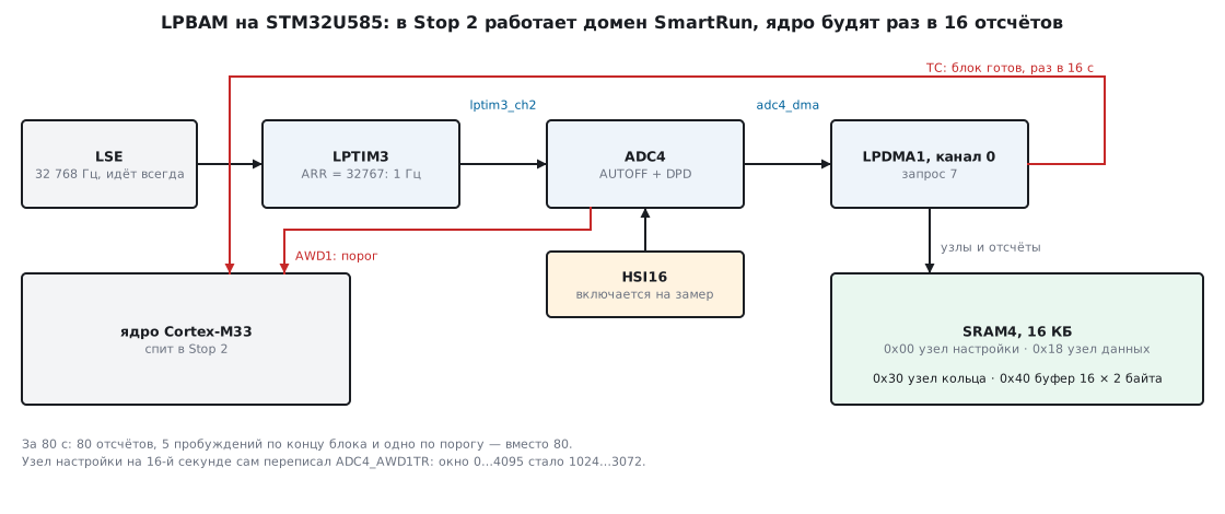
The core does not take part. It is woken by two events: the channel has collected a block, or a sample has gone beyond the threshold. The rest of the time the timer on the watch crystal works and, for microseconds once a second, the ADC with the oscillator.
A transfer to a peripheral register and a data transfer have the same mechanics. Hence the technique LPBAM rests on: a list node can write a word from memory into a configuration register of a block. RM0456 says this directly: a chain of transfers can write peripheral registers and change their configuration without leaving Stop. This is how, without the core, the ADC threshold, the timer period, the level of a pin are changed.
Stop 3 does not have this: the datasheet says that LPBAM is not supported in Stop 3.
10б.2 Who works in Stop 2 and what to enable for it
Only blocks on the AHB3 and APB3 buses are autonomous in Stop 2 (RM0456, table 116):
| Block | What it can do in Stop 2 |
|---|---|
| LPUART1, SPI3, I2C3 | exchange with transfer through LPDMA1 |
| ADC4 | measurement on a trigger, a transfer request or a threshold |
| DAC1 | output of samples from memory |
| LPTIM1, LPTIM3 | counting, PWM, capture, transfer requests |
| LPTIM4 | counting and triggering other blocks; no transfer requests |
| ADF1 | an audio filter: a stream to memory, wake-up on sound |
| LPDMA1 and SRAM4 | transfers and memory for them |
Besides these, comparators, operational amplifiers, VREFBUF, the RTC and LPGPIO1
have their own enable bit in RCC_SRDAMR. The other USART, SPI,
I²C and GPDMA1 are autonomous only in Stop 0 and Stop 1.
The documents disagree about LPTIM4: the datasheet puts it in the Stop 2 list,
section 10.7.2 of the manual does not, and table 593 clarifies: it has no autonomous
mode and no transfer requests. Its output lptim4_out, however,
is routed to the LPDMA1 trigger.
Memory. LPDMA1 is a master only on the bus of its own domain. Of memory it sees only SRAM4 — 16 KB at address 0x2800 0000. The list nodes, the buffers and the words for writing into registers lie there. It cannot reach ordinary RAM either in Stop 2 or in Run.
Three bits per block. xxEN gives the clock in Run. xxSMEN keeps it
in Sleep and Stop. xxAMEN in RCC_SRDAMR allows the block to request a clock
in Stop 2. All three are needed, and not only for the peripherals but also for LPDMA1
and SRAM4.
The block clock. In Stop 2 only oscillators that can
switch on on request or that always run are suitable. For LPTIM3 this is LSE or LSI
(LPTIM34SEL), for ADC4 HSI16 or MSIK (ADCDACSEL = 100 or 101).
LSE is given to the peripherals only with LSESYSEN = 1 in RCC_BDCR: without this
bit the crystal goes to the RTC alone.
The bus clock. Which oscillator wakes up for a transfer is selected by
STOPWUCK — the same bit that selects the core clock after Stop (10а.5).
If the oscillator start-up delay is a problem, SRDRUN in PWR_CR2 keeps
the AHB3 and APB3 clock on, and HSIKERON and MSIKERON keep the oscillator.
This is paid for in current.
10б.3 LPDMA1: request, trigger and list node
LPDMA1 has four channels without a buffer, and addressing is only linear.
The request number is put into REQSEL of the CxTR2 register (RM0456, table 146):
REQSEL |
Request | REQSEL |
Request |
|---|---|---|---|
| 0, 1 | LPUART1: receive, transmit | 8, 9 | DAC1: channels 1 and 2 |
| 2, 3 | SPI3: receive, transmit | 10 | ADF1 |
| 4, 5, 6 | I2C3: receive, transmit, event | 11, 12, 13 | LPTIM1: capture 1, capture 2, update |
| 7 | ADC4 | 14, 15, 16 | LPTIM3: capture 1, capture 2, update |
A transfer can also be held back until a trigger: TRIGSEL selects one
of 32 signals, TRIGPOL the edge. Among them are EXTI lines 0…4 (numbers
0…4), lptim1_ch1 (8), lptim3_ch1 (10), lptim4_out (11), the comparator
outputs (12, 13), RTC alarms A and B (14, 15), the threshold adc4_awd1
(17) and the transfer ends of the LPDMA1 channels themselves (18…21). This way one channel
starts another.
The node. A channel has six list registers: CTR1, CTR2, CBR1, CSAR,
CDAR, CLLR. A node in memory is the same words in the same order, but not
necessarily all of them. What to read is told by the CLLR bits of the current node:
CLLR bit |
What to load from the next node |
|---|---|
UT1, UT2 |
CTR1 (width, address step), CTR2 (request, trigger, event) |
UB1 |
CBR1 — the block length in bytes |
USA, UDA |
the source and destination addresses |
ULL |
CLLR itself — the link onward |
LA |
the offset of the next node from the CLBAR base, a multiple of 4 |
A full node is six words. If an update bit is cleared, the word is not in the node,
and the register stays as it was. CBR1 is restored by itself in this case:
the block counter returns to the programmed value. The channel
is finished when CLLR = 0. If ULL = 0 but the offset is not zero,
the link does not change, and the last node repeats forever — this is how a ring
is made.
The event. The TCEM field in CTR2 decides when to set the TCF flag:
00 — at the end of each block, 10 — at the end of a node, 11 — at the end of the whole
list. An endless list with TCEM = 11 has no event at all. Since
each node has its own CTR2, some nodes wake the core and others do not.
A configuration node. Width 4 bytes, the source is a word in SRAM4, the destination is
a register address, SWREQ = 1. Such a node does not wait for a request: the channel requests
the bus clock at once, writes the word and goes on. This is writing a register
without the core.
10б.4 Example: a measurement once a second, a wake-up once every sixteen
A sensor on input ADC4_IN1. LPTIM3 from LSE counts up to 32 767 — a period of
one second. The edge of its second channel lptim3_ch2 is the adc_trg6 trigger
of ADC4 (RM0456, table 325). The ADC is in autonomous mode: between measurements
both it and its regulator are off. Channel 0 of LPDMA1 on request 7 puts
the sample into the buffer. After 16 samples — an event and a wake-up.
To show a configuration node, the list is made of three nodes. The first
block runs with a threshold window of 0…4095: the sensor is warming up, outliers do not
wake anyone. Then the configuration node writes the working window
1024…3072 into ADC4_AWD1TR, and from then on the data block repeats in a ring. The manual
explicitly allows changing AWD1TR on the fly.
The SRAM4 layout and the node table:
#include <stddef.h>
#include "stm32u5xx.h"

#define N_SAMPLES   16u                         /* отсчётов в блоке: одно пробуждение на 16 замеров */
#define LSE_HZ      32768u
#define ARR_1HZ     (LSE_HZ - 1u)               /* период LPTIM3 — 1 с */
#define AWD_WIDE    0x0FFF0000u                 /* окно порога 0…4095: первый блок не будит */
#define AWD_TIGHT   0x0C000400u                 /* рабочее окно 1024…3072 */

/* Раскладка SRAM4: всё, что читает и пишет LPDMA1 в Stop 2, лежит здесь */
#define LLI_BASE    SRAM4_BASE                  /* в CLBAR — старшие 16 бит адреса узлов */
#define OFF_CFG     0x00u                       /* узел настройки: 6 слов */
#define OFF_DATA    0x18u                       /* узел данных: 6 слов */
#define OFF_RING    0x30u                       /* узел кольца: 1 слово, новый CDAR */
#define OFF_AWD     0x34u                       /* слово, которое узел настройки пишет в ADC4_AWD1TR */
#define OFF_BUF     0x40u                       /* буфер отсчётов, N_SAMPLES по 16 бит */

#define ADC4_DR_ADDR      (ADC4_BASE + offsetof(ADC_TypeDef, DR))
#define ADC4_AWD1TR_ADDR  (ADC4_BASE + offsetof(ADC_TypeDef, AWD1TR))

#define REQ_ADC4    7u                          /* adc4_dma, RM0456 таблица 146 */
#define TR1_DATA    (DMA_CTR1_SDW_LOG2_0 | DMA_CTR1_DDW_LOG2_0 | DMA_CTR1_DINC)   /* 16 бит -> 16 бит, приёмник с шагом */
#define TR2_DATA    (REQ_ADC4 << DMA_CTR2_REQSEL_Pos)                             /* TCEM = 00: событие в конце блока */
#define TR1_CFG     (DMA_CTR1_SDW_LOG2_1 | DMA_CTR1_DDW_LOG2_1)                   /* слово -> слово, адреса на месте */
#define TR2_CFG     (DMA_CTR2_SWREQ | DMA_CTR2_TCEM)                              /* без запроса; TCEM = 11: события нет */
#define LLR_ALL     (DMA_CLLR_UT1 | DMA_CLLR_UT2 | DMA_CLLR_UB1 | DMA_CLLR_USA | DMA_CLLR_UDA | DMA_CLLR_ULL)

/* Узлы связного списка. Порядок слов в узле — порядок регистров: TR1, TR2, BR1, SAR, DAR, LLR */
const uint32_t lli_tab[14] = {
    /* 0x00 узел настройки: 4 байта из SRAM4 в регистр порога АЦП, дальше — узел данных */
    TR1_CFG, TR2_CFG, 4u, LLI_BASE + OFF_AWD, ADC4_AWD1TR_ADDR, LLR_ALL | OFF_DATA,
    /* 0x18 узел данных: N отсчётов из ADC4_DR в буфер, дальше — узел кольца */
    TR1_DATA, TR2_DATA, 2u * N_SAMPLES, ADC4_DR_ADDR, LLI_BASE + OFF_BUF, DMA_CLLR_UDA | OFF_RING,
    /* 0x30 узел кольца: только CDAR. ULL = 0, поэтому CLLR остаётся на нём — блок повторяется вечно */
    LLI_BASE + OFF_BUF,
    /* 0x34 данные узла настройки */
    AWD_TIGHT,
};

volatile uint32_t lp_blocks;                    /* сколько блоков собрано */
volatile uint32_t lp_alarm;                     /* сработал порог */
volatile uint32_t lp_error;                     /* флаги ошибок канала */
The ring node takes one word: the data node has only
UDA and the offset 0x30 in CLLR. After each block the channel reads the buffer
address from there, restores the block length itself and leaves the link untouched.
Clocks and the domain power:
void srd_clocks_init(void)
{
    RCC->AHB3ENR |= RCC_AHB3ENR_PWREN;
    PWR->DBPR |= PWR_DBPR_DBP;                              /* открыть резервный домен: там LSE */
    RCC->BDCR |= RCC_BDCR_LSEON;
    while (!(RCC->BDCR & RCC_BDCR_LSERDY)) { }
    RCC->BDCR |= RCC_BDCR_LSESYSEN;                         /* без этого LSE достаётся только RTC */
    while (!(RCC->BDCR & RCC_BDCR_LSESYSRDY)) { }
    RCC->CR |= RCC_CR_HSION;                                /* HSI16: такт АЦП и шины в Stop 2 */
    while (!(RCC->CR & RCC_CR_HSIRDY)) { }
    RCC->CFGR1 |= RCC_CFGR1_STOPWUCK;                       /* шину в Stop будит HSI16 */

    RCC->CCIPR3 = (RCC->CCIPR3 & ~(RCC_CCIPR3_LPTIM34SEL | RCC_CCIPR3_ADCDACSEL))
                | RCC_CCIPR3_LPTIM34SEL                     /* 11: LPTIM3 от LSE */
                | RCC_CCIPR3_ADCDACSEL_2;                   /* 100: АЦП от HSI16 */

    /* три бита на каждый блок: EN — такт в Run, SMEN — в Sleep и Stop, AMEN — в Stop 2 */
    RCC->AHB3ENR   |= RCC_AHB3ENR_ADC4EN | RCC_AHB3ENR_LPDMA1EN | RCC_AHB3ENR_SRAM4EN;
    RCC->APB3ENR   |= RCC_APB3ENR_LPTIM3EN;
    RCC->AHB3SMENR |= RCC_AHB3SMENR_ADC4SMEN | RCC_AHB3SMENR_LPDMA1SMEN | RCC_AHB3SMENR_SRAM4SMEN;
    RCC->APB3SMENR |= RCC_APB3SMENR_LPTIM3SMEN;
    RCC->SRDAMR    |= RCC_SRDAMR_ADC4AMEN | RCC_SRDAMR_LPDMA1AMEN | RCC_SRDAMR_SRAM4AMEN
                    | RCC_SRDAMR_LPTIM3AMEN;

    PWR->CR2 &= ~PWR_CR2_SRAM4PDS;                          /* SRAM4 в Stop не выключать */
}
The timer and the ADC:
void lptim3_init(void)
{
    LPTIM3->CFGR = 0;                                       /* внутренний такт, делитель 1, пуск программный */
    LPTIM3->CCMR1 = 0;                                      /* канал 2 — выход, полярность прямая */
    LPTIM3->CR = LPTIM_CR_ENABLE;                           /* ARR и CCR2 пишут только при ENABLE = 1 */
    LPTIM3->ICR = LPTIM_ICR_ARROKCF | LPTIM_ICR_CMP2OKCF;
    LPTIM3->ARR = ARR_1HZ;
    while (!(LPTIM3->ISR & LPTIM_ISR_ARROK)) { }
    LPTIM3->CCR2 = ARR_1HZ / 2u;                            /* фронт lptim3_ch2 раз в период */
    while (!(LPTIM3->ISR & LPTIM_ISR_CMP2OK)) { }
    LPTIM3->CCMR1 |= LPTIM_CCMR1_CC2E;
    LPTIM3->CR |= LPTIM_CR_CNTSTRT;                         /* непрерывный счёт */
}

void adc4_init(void)
{
    ADC4->ISR = ADC_ISR_LDORDY;                             /* флаги сбрасывают записью 1 */
    ADC4->CR = ADC_CR_ADVREGEN;
    while (!(ADC4->ISR & ADC_ISR_LDORDY)) { }
    ADC4->CR |= ADC_CR_ADCAL;                               /* калибровка: ADEN = 0, AUTOFF = 0, DMAEN = 0 */
    while (ADC4->CR & ADC_CR_ADCAL) { }

    ADC4->CFGR1 = ADC4_CFGR1_DMAEN | ADC4_CFGR1_DMACFG      /* запрос на каждый отсчёт, без остановки */
                | ADC_CFGR1_EXTEN_0                         /* запуск по фронту */
                | ADC4_CFGR1_EXTSEL_2 | ADC4_CFGR1_EXTSEL_1 /* 110: adc_trg6 = lptim3_ch2 */
                | ADC_CFGR1_AWD1EN | ADC_CFGR1_AWD1SGL | ADC_CFGR1_AWD1CH_0;   /* порог на канале 1 */
    ADC4->SMPR1 = ADC4_SMPR_SMP1_2;                         /* ADC_SMPR в RM0456; 100: выборка 19,5 такта */
    ADC4->CHSELR = ADC_CHSELR_CHSEL1;                       /* ADC4_IN1 */
    ADC4->AWD1TR = AWD_WIDE;
    ADC4->ISR = ADC_ISR_AWD1;
    ADC4->IER = ADC_IER_AWD1IE;                             /* будить по порогу, а не по каждому отсчёту */
    ADC4->PWRR = ADC4_PWRR_AUTOFF | ADC4_PWRR_DPD;          /* автономный режим: между замерами выключен */
    ADC4->CR |= ADC_CR_ADEN;                                /* ADRDY при AUTOFF = 1 не взводится — не ждём */
    ADC4->CR |= ADC_CR_ADSTART;                             /* дальше замеры идут по lptim3_ch2 */
    NVIC_EnableIRQ(ADC4_IRQn);
}
For ADC4 the CMSIS header calls the sampling register SMPR1, although
in the manual it is ADC_SMPR: the ADC_TypeDef structure is shared by ADC1 and ADC4.
The ADC4 fields, however, have the prefix ADC4_: EXTSEL in ADC4 has three
bits from the sixth, ADC1 has five from the fifth.
The channel and interrupts:
void lpdma_start(void)
{
    uint32_t *mem = (uint32_t *)LLI_BASE;
    uint32_t i;

    for (i = 0; i < sizeof lli_tab / sizeof lli_tab[0]; i++) {
        mem[i] = lli_tab[i];                                /* узлы — в SRAM4: другой памяти LPDMA1 не видит */
    }

    LPDMA1_Channel0->CCR = DMA_CCR_RESET;
    LPDMA1_Channel0->CFCR = DMA_CFCR_TCF | DMA_CFCR_HTF | DMA_CFCR_DTEF | DMA_CFCR_ULEF
                          | DMA_CFCR_USEF | DMA_CFCR_SUSPF | DMA_CFCR_TOF;
    LPDMA1_Channel0->CLBAR = LLI_BASE;
    /* нулевой элемент списка живёт прямо в регистрах канала: первый блок данных */
    LPDMA1_Channel0->CTR1 = TR1_DATA;
    LPDMA1_Channel0->CTR2 = TR2_DATA;
    LPDMA1_Channel0->CBR1 = 2u * N_SAMPLES;
    LPDMA1_Channel0->CSAR = ADC4_DR_ADDR;
    LPDMA1_Channel0->CDAR = LLI_BASE + OFF_BUF;
    LPDMA1_Channel0->CLLR = LLR_ALL | OFF_CFG;              /* после блока — узел настройки */
    LPDMA1_Channel0->CCR = DMA_CCR_TCIE | DMA_CCR_DTEIE | DMA_CCR_ULEIE | DMA_CCR_USEIE;
    NVIC_EnableIRQ(LPDMA1_Channel0_IRQn);
    LPDMA1_Channel0->CCR |= DMA_CCR_EN;
}

void LPDMA1_Channel0_IRQHandler(void)
{
    uint32_t sr = LPDMA1_Channel0->CSR;

    if (sr & DMA_CSR_TCF) {
        lp_blocks++;                                        /* буфер полон: N отсчётов */
    }
    if (sr & (DMA_CSR_DTEF | DMA_CSR_ULEF | DMA_CSR_USEF)) {
        lp_error = sr;                                      /* канал остановлен аппаратно */
    }
    /* пока флаг не сброшен, LPDMA1 держит запрос такта и Stop 2 остаётся с включённым генератором */
    LPDMA1_Channel0->CFCR = sr & (DMA_CFCR_TCF | DMA_CFCR_DTEF | DMA_CFCR_ULEF | DMA_CFCR_USEF);
}

void ADC4_IRQHandler(void)
{
    if (ADC4->ISR & ADC_ISR_AWD1) {
        ADC4->ISR = ADC_ISR_AWD1;
        lp_alarm = 1;
    }
}
Entering Stop 2 and the main loop:
void stop2_enter(void)
{
    PWR->CR1 = (PWR->CR1 & ~PWR_CR1_LPMS) | PWR_CR1_LPMS_1; /* 010 — Stop 2; в Stop 3 LPBAM нет */
    SCB->SCR |= SCB_SCR_SLEEPDEEP_Msk;
    __DSB();
    __WFI();
    SCB->SCR &= ~SCB_SCR_SLEEPDEEP_Msk;
}

uint32_t block_mean(void)
{
    const volatile uint16_t *buf = (const volatile uint16_t *)(LLI_BASE + OFF_BUF);
    uint32_t sum = 0, i;

    for (i = 0; i < N_SAMPLES; i++) {
        sum += buf[i];
    }
    return sum / N_SAMPLES;
}

int main(void)
{
    uint32_t done = 0;
    volatile uint32_t mean = 0;

    srd_clocks_init();
    lptim3_init();
    adc4_init();
    lpdma_start();

    for (;;) {
        stop2_enter();                                      /* 16 замеров проходят без ядра */
        if (lp_blocks != done) {
            done = lp_blocks;
            mean = block_mean();                            /* здесь — обработка блока */
        }
        if (lp_alarm || lp_error) {
            lp_alarm = 0;                                   /* здесь — реакция на порог или ошибку */
        }
        (void)mean;
    }
}
10б.5 A run: what the channel does second by second
A board is not needed to check the list itself. The check builds the firmware,
extracts the lli_tab array from the object file and gives it to a model of the channel:
six registers, loading by the CLLR bits, restoring CBR1, TCEM,
alignment checks and checks that all addresses are in SRAM4 or in the
SmartRun domain. The compiler put 14 words, 56 bytes, into the table:
| Node | TR1 |
TR2 |
BR1 |
SAR |
DAR |
LLR |
|---|---|---|---|---|---|---|
| configuration, 0x00 | 0x00020002 | 0xC0000200 | 4 | 0x28000034 | 0x46021020 | 0xF8010018 |
| data, 0x18 | 0x00090001 | 0x00000007 | 32 | 0x46021040 | 0x28000040 | 0x08000030 |
| ring, 0x30 | — | — | — | — | 0x28000040 | — |
0x46021020 is ADC4_AWD1TR, 0x46021040 is ADC4_DR. The model feeds
a sample once a second, and at the 5th and 50th second an outlier of 3500:
  5 с  отсчёт 3500 в окне 0…4095: порог молчит
 16 с  блок из 16 отсчётов готов
    подгрузка узла 0x00: TR1=0x00020002, TR2=0xC0000200, BR1=0x00000004, SAR=0x28000034, DAR=0x46021020, LLR=0xF8010018
 16 с  событие TC: ядро разбужено
 16 с  узел настройки: ADC4_AWD1TR <- 0x0C000400 (окно 1024…3072)
    подгрузка узла 0x18: TR1=0x00090001, TR2=0x00000007, BR1=0x00000020, SAR=0x46021040, DAR=0x28000040, LLR=0x08000030
 32 с  блок из 16 отсчётов готов
    подгрузка узла 0x30: DAR=0x28000040
 32 с  событие TC: ядро разбужено
 48 с  блок из 16 отсчётов готов
    подгрузка узла 0x30: DAR=0x28000040
 48 с  событие TC: ядро разбужено
 50 с  отсчёт 3500 вне окна 1024…3072: прерывание AWD1, ядро разбужено
 64 с  блок из 16 отсчётов готов
    подгрузка узла 0x30: DAR=0x28000040
 64 с  событие TC: ядро разбужено
 80 с  блок из 16 отсчётов готов
    подгрузка узла 0x30: DAR=0x28000040
 80 с  событие TC: ядро разбужено

за 80 с: отсчётов 80, пробуждений по TC 5 (секунды 16,32,48,64,80), по порогу 1 (секунда 50)
без LPDMA1 пробуждений было бы 80
регистры канала в конце: BR1=32 DAR=0x28000040 LLR=0x08000030 EN=1
Eighty measurements — five wake-ups by block and one by threshold.
The outlier at the 5th second fell into the wide window and woke no one.
At the 16th the configuration node narrowed the window, and the same outlier at the 50th woke
the core at once, without waiting for the end of the block. After five blocks the channel
registers hold CLLR = 0x08000030 and CDAR = 0x28000040: the ring is closed.
The firmware builds with gcc and armclang without warnings; with gcc -Os
the code together with the table is 828 bytes, the variables 12 bytes. The node tables
of both compilers matched byte for byte.
Comparison with ST. The word order in a node is the same as in the HAL driver
(stm32u5xx_hal_dma_ex.h). License: BSD-3-Clause. The offsets there are:
CTR1 — 0, CTR2 — 1, CBR1 — 2, CSAR — 3, CDAR — 4, CLLR with
linear addressing — 5. The pack does not contain the LPBAM utility itself. The
STM32CubeMX database has its calls for eleven blocks — ADC, COMP, DAC,
I2C, LPDMA, LPGPIO, LPTIM, LPUART, OPAMP, SPI, VREFBUF — of three kinds:
…_SetConfigQ, …_SetDataQ and …_SetFullQ, for example
ADV_LPBAM_ADC_Conversion_SetConfigQ. Judging by the names these are queues of configuration
nodes, data nodes and both together. There is nothing to check the layout of its nodes
against: the sources of the utility are not in the pack.
10б.6 The budget: when LPBAM pays off
Let us compare two devices on the same chip. Both sleep in Stop 2 and measure at a rate f. The first wakes the core for every sample, the second once every N samples. Processing a sample costs the same whenever it is done, so the difference is only in the overhead of waking up:
Q_п  = Q_wu + I_run · t_н                 заряд одного пробуждения
I_А  = I_0 + f · Q_п                      будить на каждый отсчёт
I_Б  = I_0 + I_SRAM4 + f · Q_отсч + (f / N) · Q_п
I_А − I_Б = f · Q_п · (1 − 1/N) − I_SRAM4 − f · Q_отсч
From the datasheet, 3 V, 25 °C, the LDO regulator: Stop 2 — 9.05 µA; SRAM4 in Stop 2 — another 0.3 µA; the wake-up charge from Stop 2 on HSI16 — 30 nA·s; Run at 16 MHz in range 4 — 1.30 mA; LPTIM3 from an independent clock — 2.19 µA/MHz, on LSE this is 0.072 µA. The common part I_0 is 9.12 µA.
Two numbers are not in the datasheet. t_n is how long the core stays awake for one wake-up beyond the processing itself: interrupt entry, flags, returning to Stop. This is an assumption; 100 µs and 1 ms are taken. Q_otsch is the charge of one autonomous measurement with its transfer; it is not specified, and the model calculates the reverse: at what Q_otsch the second device still wins.
| t_n and Q_p | f | Wake for every sample | Gain ceiling, N = 16 | Threshold Q_otsch |
|---|---|---|---|---|
| 100 µs, 160 nA·s | 1 Hz | 9.28 µA | −0.15 µA | no gain |
| 100 µs, 160 nA·s | 10 Hz | 10.72 µA | +1.20 µA | 120.0 nA·s |
| 100 µs, 160 nA·s | 100 Hz | 25.12 µA | +14.70 µA | 147.0 nA·s |
| 1 ms, 1330 nA·s | 1 Hz | 10.45 µA | +0.95 µA | 946.9 nA·s |
| 1 ms, 1330 nA·s | 10 Hz | 22.42 µA | +12.17 µA | 1216.9 nA·s |
| 1 ms, 1330 nA·s | 100 Hz | 142.12 µA | +124.39 µA | 1243.9 nA·s |
The ceiling is the gain with a free measurement; you cannot get more.
The conclusion is the same as in 10а, only from the other side. With one measurement a second and a short wake-up, waking the core costs 0.16 µA, while SRAM4 alone costs 0.3 µA: LPBAM loses, even if the measurement itself costs nothing. It pays off when there are many wake-ups or they are long: at 100 Hz a core woken for every sample takes 25.12 µA against 9.12, and almost all of it comes back.
Of Q_otsch itself one component is known. A conversion with a sampling time of 19.5 cycles lasts (19.5 + 12 + 0.5) / 16 MHz = 2.0 µs, the ADC regulator starts up within 25 µs, HSI16 takes 150 µA: that is 4.05 nA·s. The ADC and bus current are not included here. Only measurements on a board give the real number — the three measurements from 10.8, with LPBAM and without.
10б.7 Pitfalls
Nodes or the buffer are not in SRAM4. LPDMA1 does not see other memory: according to the manual, SRAM4 is the only RAM accessible to it. An array of nodes declared as an ordinary variable will end up in the wrong place — that is why the firmware copies the table to the SRAM4 address itself.
AMEN is forgotten. The block is enabled, works in Sleep, but is silent in Stop 2.
You need EN, SMEN and AMEN — for the peripheral, for LPDMA1 and for SRAM4.
LSE is there, LPTIM3 stands still. LSESYSEN is not set: the crystal clocks
only the RTC.
The ADC clock from the bus. ADCDACSEL = 000 is the HCLK clock. In Stop 2 ADC4
works only from HSI16 or MSIK.
The channel flag is not cleared. While TCF is pending, LPDMA1 holds the clock request:
the chip is in Stop 2, but the oscillator runs. The same if a block's interrupt
is enabled but not in the NVIC: the manual explicitly forbids this.
Stop 2 does not happen at once. If a block requests a clock at the moment of WFI,
entry into Stop is postponed until the end of the request.
Waiting for ADRDY with AUTOFF. In auto-off mode the ready flag
is not set; a waiting loop will hang.
Calibration after AUTOFF. Calibrate with AUTOFF = 0, DPD = 0
and DMAEN = 0, and enable the mode afterwards.
DMACFG = 0 with a ring. In one-shot mode the ADC stops requesting
transfers when the controller has finished the block. A ring needs
DMACFG = 1.
ARR before ENABLE. ARR and CCR2 of LPTIM are written only with the timer
enabled, CFGR only with it disabled.
Changing any ADC register with a configuration node. On the fly the manual
allows changing only the AWDxTR thresholds. The channel, the sampling time and the trigger
are changed with ADSTART = 0.
Stop 3 instead of Stop 2. The sleep current is lower, but there is no LPBAM there.
TrustZone. With TZEN = 1, for secure software SRAM4 and the peripherals
lie at other addresses (SRAM4 — 0x3800 0000), and the transfer gets the
bits SSEC and DSEC. The example is written for TZEN = 0.
LPBAM for the sake of 1 Hz. With rare measurements SRAM4 alone costs more than the wake-ups saved.
10б.8 Summary
- LPBAM is the autonomous peripherals of the SmartRun domain, LPDMA1 with a linked list, and hardware triggers. It works in Stop 0, 1 and 2; in Stop 3 it does not.
- In Stop 2 LPUART1, SPI3, I2C3, ADC4, DAC1, LPTIM1, LPTIM3, ADF1 are autonomous; the transfer memory is only SRAM4, 16 KB.
- Each block, LPDMA1 and SRAM4 need three bits:
EN,SMEN,AMEN. - A list node is up to six words:
CTR1,CTR2,CBR1,CSAR,CDAR,CLLR. The bitsUT1…ULLsay which words are in the node. A ring is a node withULL= 0. - A node with
SWREQ= 1 writes a word from SRAM4 into a peripheral register — this is how a block is reconfigured without the core. - The example: LPTIM3 starts ADC4 once a second, channel 0 accumulates 16 samples. In 80 s — 5 wake-ups by block and 1 by threshold instead of 80. The node table is 56 bytes, the code 828 bytes.
- The ADC4 request is number 7; triggering ADC4 from LPTIM3 is
adc_trg6, the second channel of the timer. - Stop 2 — 9.05 µA, SRAM4 — plus 0.3 µA, a wake-up — 30 nA·s. At 1 Hz and an overhead of 100 µs LPBAM loses 0.15 µA; at 100 Hz the gain ceiling is 14.70 µA out of 25.12.
Full sources
lpbam10b.c — LPTIM3 → ADC4 → LPDMA1 → SRAM4 in Stop 2: the core wakes up once per block of samples.
/* Раздел 10б. LPTIM3 -> ADC4 -> LPDMA1 -> SRAM4 в Stop 2: ядро просыпается раз в N отсчётов.
 * STM32U585, заголовок CMSIS stm32u585xx.h, TrustZone выключен (TZEN = 0).
 * Сборка: arm-none-eabi-gcc -mcpu=cortex-m33 -mthumb -Os -DSTM32U585xx -c lpbam10b.c */
#include <stddef.h>
#include "stm32u5xx.h"

#define N_SAMPLES   16u                         /* отсчётов в блоке: одно пробуждение на 16 замеров */
#define LSE_HZ      32768u
#define ARR_1HZ     (LSE_HZ - 1u)               /* период LPTIM3 — 1 с */
#define AWD_WIDE    0x0FFF0000u                 /* окно порога 0…4095: первый блок не будит */
#define AWD_TIGHT   0x0C000400u                 /* рабочее окно 1024…3072 */

/* Раскладка SRAM4: всё, что читает и пишет LPDMA1 в Stop 2, лежит здесь */
#define LLI_BASE    SRAM4_BASE                  /* в CLBAR — старшие 16 бит адреса узлов */
#define OFF_CFG     0x00u                       /* узел настройки: 6 слов */
#define OFF_DATA    0x18u                       /* узел данных: 6 слов */
#define OFF_RING    0x30u                       /* узел кольца: 1 слово, новый CDAR */
#define OFF_AWD     0x34u                       /* слово, которое узел настройки пишет в ADC4_AWD1TR */
#define OFF_BUF     0x40u                       /* буфер отсчётов, N_SAMPLES по 16 бит */

#define ADC4_DR_ADDR      (ADC4_BASE + offsetof(ADC_TypeDef, DR))
#define ADC4_AWD1TR_ADDR  (ADC4_BASE + offsetof(ADC_TypeDef, AWD1TR))

#define REQ_ADC4    7u                          /* adc4_dma, RM0456 таблица 146 */
#define TR1_DATA    (DMA_CTR1_SDW_LOG2_0 | DMA_CTR1_DDW_LOG2_0 | DMA_CTR1_DINC)   /* 16 бит -> 16 бит, приёмник с шагом */
#define TR2_DATA    (REQ_ADC4 << DMA_CTR2_REQSEL_Pos)                             /* TCEM = 00: событие в конце блока */
#define TR1_CFG     (DMA_CTR1_SDW_LOG2_1 | DMA_CTR1_DDW_LOG2_1)                   /* слово -> слово, адреса на месте */
#define TR2_CFG     (DMA_CTR2_SWREQ | DMA_CTR2_TCEM)                              /* без запроса; TCEM = 11: события нет */
#define LLR_ALL     (DMA_CLLR_UT1 | DMA_CLLR_UT2 | DMA_CLLR_UB1 | DMA_CLLR_USA | DMA_CLLR_UDA | DMA_CLLR_ULL)

/* Узлы связного списка. Порядок слов в узле — порядок регистров: TR1, TR2, BR1, SAR, DAR, LLR */
const uint32_t lli_tab[14] = {
    /* 0x00 узел настройки: 4 байта из SRAM4 в регистр порога АЦП, дальше — узел данных */
    TR1_CFG, TR2_CFG, 4u, LLI_BASE + OFF_AWD, ADC4_AWD1TR_ADDR, LLR_ALL | OFF_DATA,
    /* 0x18 узел данных: N отсчётов из ADC4_DR в буфер, дальше — узел кольца */
    TR1_DATA, TR2_DATA, 2u * N_SAMPLES, ADC4_DR_ADDR, LLI_BASE + OFF_BUF, DMA_CLLR_UDA | OFF_RING,
    /* 0x30 узел кольца: только CDAR. ULL = 0, поэтому CLLR остаётся на нём — блок повторяется вечно */
    LLI_BASE + OFF_BUF,
    /* 0x34 данные узла настройки */
    AWD_TIGHT,
};

volatile uint32_t lp_blocks;                    /* сколько блоков собрано */
volatile uint32_t lp_alarm;                     /* сработал порог */
volatile uint32_t lp_error;                     /* флаги ошибок канала */

void srd_clocks_init(void)
{
    RCC->AHB3ENR |= RCC_AHB3ENR_PWREN;
    PWR->DBPR |= PWR_DBPR_DBP;                              /* открыть резервный домен: там LSE */
    RCC->BDCR |= RCC_BDCR_LSEON;
    while (!(RCC->BDCR & RCC_BDCR_LSERDY)) { }
    RCC->BDCR |= RCC_BDCR_LSESYSEN;                         /* без этого LSE достаётся только RTC */
    while (!(RCC->BDCR & RCC_BDCR_LSESYSRDY)) { }
    RCC->CR |= RCC_CR_HSION;                                /* HSI16: такт АЦП и шины в Stop 2 */
    while (!(RCC->CR & RCC_CR_HSIRDY)) { }
    RCC->CFGR1 |= RCC_CFGR1_STOPWUCK;                       /* шину в Stop будит HSI16 */

    RCC->CCIPR3 = (RCC->CCIPR3 & ~(RCC_CCIPR3_LPTIM34SEL | RCC_CCIPR3_ADCDACSEL))
                | RCC_CCIPR3_LPTIM34SEL                     /* 11: LPTIM3 от LSE */
                | RCC_CCIPR3_ADCDACSEL_2;                   /* 100: АЦП от HSI16 */

    /* три бита на каждый блок: EN — такт в Run, SMEN — в Sleep и Stop, AMEN — в Stop 2 */
    RCC->AHB3ENR   |= RCC_AHB3ENR_ADC4EN | RCC_AHB3ENR_LPDMA1EN | RCC_AHB3ENR_SRAM4EN;
    RCC->APB3ENR   |= RCC_APB3ENR_LPTIM3EN;
    RCC->AHB3SMENR |= RCC_AHB3SMENR_ADC4SMEN | RCC_AHB3SMENR_LPDMA1SMEN | RCC_AHB3SMENR_SRAM4SMEN;
    RCC->APB3SMENR |= RCC_APB3SMENR_LPTIM3SMEN;
    RCC->SRDAMR    |= RCC_SRDAMR_ADC4AMEN | RCC_SRDAMR_LPDMA1AMEN | RCC_SRDAMR_SRAM4AMEN
                    | RCC_SRDAMR_LPTIM3AMEN;

    PWR->CR2 &= ~PWR_CR2_SRAM4PDS;                          /* SRAM4 в Stop не выключать */
}

void lptim3_init(void)
{
    LPTIM3->CFGR = 0;                                       /* внутренний такт, делитель 1, пуск программный */
    LPTIM3->CCMR1 = 0;                                      /* канал 2 — выход, полярность прямая */
    LPTIM3->CR = LPTIM_CR_ENABLE;                           /* ARR и CCR2 пишут только при ENABLE = 1 */
    LPTIM3->ICR = LPTIM_ICR_ARROKCF | LPTIM_ICR_CMP2OKCF;
    LPTIM3->ARR = ARR_1HZ;
    while (!(LPTIM3->ISR & LPTIM_ISR_ARROK)) { }
    LPTIM3->CCR2 = ARR_1HZ / 2u;                            /* фронт lptim3_ch2 раз в период */
    while (!(LPTIM3->ISR & LPTIM_ISR_CMP2OK)) { }
    LPTIM3->CCMR1 |= LPTIM_CCMR1_CC2E;
    LPTIM3->CR |= LPTIM_CR_CNTSTRT;                         /* непрерывный счёт */
}

void adc4_init(void)
{
    ADC4->ISR = ADC_ISR_LDORDY;                             /* флаги сбрасывают записью 1 */
    ADC4->CR = ADC_CR_ADVREGEN;
    while (!(ADC4->ISR & ADC_ISR_LDORDY)) { }
    ADC4->CR |= ADC_CR_ADCAL;                               /* калибровка: ADEN = 0, AUTOFF = 0, DMAEN = 0 */
    while (ADC4->CR & ADC_CR_ADCAL) { }

    ADC4->CFGR1 = ADC4_CFGR1_DMAEN | ADC4_CFGR1_DMACFG      /* запрос на каждый отсчёт, без остановки */
                | ADC_CFGR1_EXTEN_0                         /* запуск по фронту */
                | ADC4_CFGR1_EXTSEL_2 | ADC4_CFGR1_EXTSEL_1 /* 110: adc_trg6 = lptim3_ch2 */
                | ADC_CFGR1_AWD1EN | ADC_CFGR1_AWD1SGL | ADC_CFGR1_AWD1CH_0;   /* порог на канале 1 */
    ADC4->SMPR1 = ADC4_SMPR_SMP1_2;                         /* ADC_SMPR в RM0456; 100: выборка 19,5 такта */
    ADC4->CHSELR = ADC_CHSELR_CHSEL1;                       /* ADC4_IN1 */
    ADC4->AWD1TR = AWD_WIDE;
    ADC4->ISR = ADC_ISR_AWD1;
    ADC4->IER = ADC_IER_AWD1IE;                             /* будить по порогу, а не по каждому отсчёту */
    ADC4->PWRR = ADC4_PWRR_AUTOFF | ADC4_PWRR_DPD;          /* автономный режим: между замерами выключен */
    ADC4->CR |= ADC_CR_ADEN;                                /* ADRDY при AUTOFF = 1 не взводится — не ждём */
    ADC4->CR |= ADC_CR_ADSTART;                             /* дальше замеры идут по lptim3_ch2 */
    NVIC_EnableIRQ(ADC4_IRQn);
}

void lpdma_start(void)
{
    uint32_t *mem = (uint32_t *)LLI_BASE;
    uint32_t i;

    for (i = 0; i < sizeof lli_tab / sizeof lli_tab[0]; i++) {
        mem[i] = lli_tab[i];                                /* узлы — в SRAM4: другой памяти LPDMA1 не видит */
    }

    LPDMA1_Channel0->CCR = DMA_CCR_RESET;
    LPDMA1_Channel0->CFCR = DMA_CFCR_TCF | DMA_CFCR_HTF | DMA_CFCR_DTEF | DMA_CFCR_ULEF
                          | DMA_CFCR_USEF | DMA_CFCR_SUSPF | DMA_CFCR_TOF;
    LPDMA1_Channel0->CLBAR = LLI_BASE;
    /* нулевой элемент списка живёт прямо в регистрах канала: первый блок данных */
    LPDMA1_Channel0->CTR1 = TR1_DATA;
    LPDMA1_Channel0->CTR2 = TR2_DATA;
    LPDMA1_Channel0->CBR1 = 2u * N_SAMPLES;
    LPDMA1_Channel0->CSAR = ADC4_DR_ADDR;
    LPDMA1_Channel0->CDAR = LLI_BASE + OFF_BUF;
    LPDMA1_Channel0->CLLR = LLR_ALL | OFF_CFG;              /* после блока — узел настройки */
    LPDMA1_Channel0->CCR = DMA_CCR_TCIE | DMA_CCR_DTEIE | DMA_CCR_ULEIE | DMA_CCR_USEIE;
    NVIC_EnableIRQ(LPDMA1_Channel0_IRQn);
    LPDMA1_Channel0->CCR |= DMA_CCR_EN;
}

void LPDMA1_Channel0_IRQHandler(void)
{
    uint32_t sr = LPDMA1_Channel0->CSR;

    if (sr & DMA_CSR_TCF) {
        lp_blocks++;                                        /* буфер полон: N отсчётов */
    }
    if (sr & (DMA_CSR_DTEF | DMA_CSR_ULEF | DMA_CSR_USEF)) {
        lp_error = sr;                                      /* канал остановлен аппаратно */
    }
    /* пока флаг не сброшен, LPDMA1 держит запрос такта и Stop 2 остаётся с включённым генератором */
    LPDMA1_Channel0->CFCR = sr & (DMA_CFCR_TCF | DMA_CFCR_DTEF | DMA_CFCR_ULEF | DMA_CFCR_USEF);
}

void ADC4_IRQHandler(void)
{
    if (ADC4->ISR & ADC_ISR_AWD1) {
        ADC4->ISR = ADC_ISR_AWD1;
        lp_alarm = 1;
    }
}

void stop2_enter(void)
{
    PWR->CR1 = (PWR->CR1 & ~PWR_CR1_LPMS) | PWR_CR1_LPMS_1; /* 010 — Stop 2; в Stop 3 LPBAM нет */
    SCB->SCR |= SCB_SCR_SLEEPDEEP_Msk;
    __DSB();
    __WFI();
    SCB->SCR &= ~SCB_SCR_SLEEPDEEP_Msk;
}

uint32_t block_mean(void)
{
    const volatile uint16_t *buf = (const volatile uint16_t *)(LLI_BASE + OFF_BUF);
    uint32_t sum = 0, i;

    for (i = 0; i < N_SAMPLES; i++) {
        sum += buf[i];
    }
    return sum / N_SAMPLES;
}

int main(void)
{
    uint32_t done = 0;
    volatile uint32_t mean = 0;

    srd_clocks_init();
    lptim3_init();
    adc4_init();
    lpdma_start();

    for (;;) {
        stop2_enter();                                      /* 16 замеров проходят без ядра */
        if (lp_blocks != done) {
            done = lp_blocks;
            mean = block_mean();                            /* здесь — обработка блока */
        }
        if (lp_alarm || lp_error) {
            lp_alarm = 0;                                   /* здесь — реакция на порог или ошибку */
        }
        (void)mean;
    }
}
Next: section 11 "Memory, linking, loading" — where everything lies,
how a linker script is built and what happens between applying power
and the call to main.