 Embedded HandbookApps
55. Linear regulators
The most common power chip on a microcontroller board. Three pins, two capacitors — and you have 3.3 volts. Precisely because of this simplicity it gets fitted without thinking, and precisely because of that it most often turns out to be the place where the board heats up, where the battery drains and where the noise in the ADC comes from.
This section is about what you need to calculate before fitting one: the headroom, the heat, the quiescent current and the output capacitor.
Terms used in the documentation
Term Meaning linear regulator a regulator that burns the excess voltage as heat low-dropout regulator (LDO) a linear regulator that needs little headroom dropout voltage the minimum input-output difference pass element the controlled transistor in series with the load adjustable / fixed output output set by a divider / output set inside reference voltage the internal voltage the output is compared to quiescent current (Iq), ground current the regulator's own current consumption load / line regulation output change with load / with input voltage power supply rejection ratio (PSRR) how much input noise is suppressed junction temperature (Tj) the temperature of the die thermal resistance (Rth) temperature rise per watt dissipated thermal shutdown switching off on overheating equivalent series resistance (ESR) the internal series resistance of a capacitor
55.1 How it works
Inside there is a pass element (essentially a controlled resistance) in series with the load, a voltage reference and an error amplifier that opens the element just enough for the output to match the reference. It is the same feedback loop as in section 47, only entirely inside the package.
All the properties follow at once: the output is always lower than the input; the difference turns into heat; the input current equals the output current plus the regulator's own.
55.2 Fixed and adjustable
Fixed output — three pins, the value is built in. The circuit around it: a capacitor at the input, a capacitor at the output. For 3.3 and 5 V these are the ones used.
An adjustable one holds the reference voltage on its feedback pin
(1.25 V for the classic part) and lets you set the output with a
divider: Vout = Vref · (1 + R2/R1) + Iadj · R2, where Iadj is the current of the adjust
pin, about 50 µA. With R2 = 390 Ω that is +20 mV; with a divider
of tens of kilohms, hundreds of millivolts: one more reason to keep it low-impedance.
For 3.3 V with a 240 Ω lower leg the upper leg should be 393.6 Ω; from the E24 series you take 390 Ω and get 3.281 V — 19 mV off, six tenths of a percent. The next value, 430 Ω, would already give 3.490 V, 190 mV too high.
⚠️ Accuracy is set by the reference, not the resistors. A ±2 % spread of the reference voltage gives an output from 3.216 to 3.347 V — 131 mV, almost seven times the error from the resistor series (19 mV). Using resistors with a 1 % tolerance makes sense, but they will not work miracles.
The lower leg is not chosen arbitrarily: the current through the divider (here 5.21 mA) serves as the minimum load — without it the classic adjustable regulator does not hold its output. A constant 17 mW that is often forgotten with battery power.
55.3 Input-output headroom: how an LDO differs
A regulator needs headroom between input and output. For the classic part it is about 2 V, for a low-dropout device 0.2 V or less.
The difference is decisive with battery power. A lithium cell gives 4.2 V charged and 3.0 V discharged:
| Regulator | Input needed | What you get |
|---|---|---|
| classic | 5.3 V | does not work at all — even a full charge gives no headroom |
| low-dropout 0.2 V | 3.5 V | exactly 3.3 V — until the battery drops to 3.5 V: by then about 85 % of the capacity has been used; below that the output follows the input minus 0.2 V |
| low-dropout 50 mV | 3.35 V | exactly 3.3 V — down to 3.35 V, about 92 % of the capacity |
The percentages come from the open-circuit table of a lithium cell in section 121, not from a straight line between 4.2 and 3.0 V. The discharge curve is non-linear: most of the capacity is delivered on the 3.6–3.8 V plateau, and by 3.5 V about 85 % of it is already used. The difference between a 0.2 V and a 50 mV dropout is about seven percent, and under load the voltage is lower than open-circuit, so both thresholds come a little earlier. More important is something else: below the threshold the regulator does not switch off — the output follows the input minus the dropout, and the microcontroller keeps running down to its reset threshold. What decides is whether the rest of the circuit tolerates the reduced supply.
55.4 Thermal calculation: the one thing you cannot skip
The power is trivial to calculate: P = (Vin − Vout) × I. Then comes
the step that is skipped most often — the junction temperature:
Tj = Tокр + P × Rth
The thermal resistance depends on the package and on how much copper is under it. The die limit is usually 125 °C.
Case one: 5 → 3.3 V at 150 mA. Power 0.255 W.
| Package | Rth | Die at 40 °C ambient |
|---|---|---|
| SOT-23 | 250 °C/W | 104 °C — works, 21 degrees of margin |
| SOT-223 | 60 °C/W | 55 °C — a large margin |
SOT-23 seems to pass. But at 85 °C ambient (a cabinet, summer, an enclosure without ventilation) it can handle only 0.16 W — less than required, and the same circuit stops working. The thermal calculation is done for the maximum ambient temperature, not room temperature.
Case two: 12 → 5 V at 500 mA. Power 3.5 W.
A TO-220 package without a heatsink gives 257 °C — the device will simply shut down on overheating. You need a thermal path no worse than 24.3 °C/W; a 5 °C/W heatsink does the job with margin. Add "junction to case" and the pad to it — together about 5 °C/W, the whole path 10 °C/W, and the die will be at 75 °C.
And the question arises at once: is it worth it? A switching converter at the same point loses 12.6 times less (section 53.4). The heatsink, the board space and the heating of the enclosure are the price of simplicity.
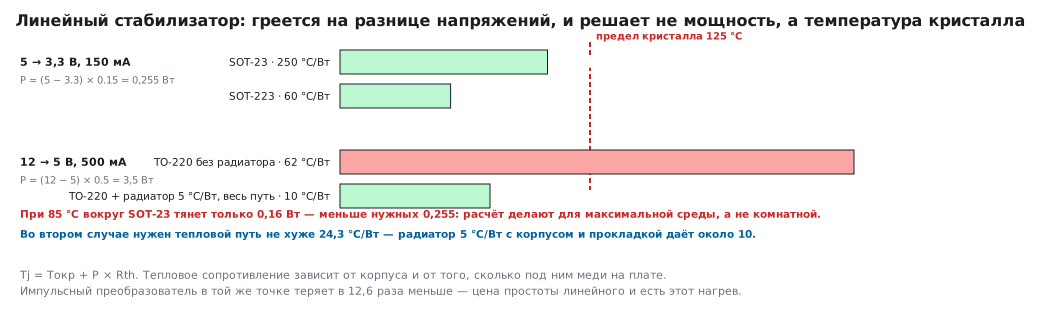
The "LDO" tab in the app's calculators computes the same for your own voltages, current, ambient and package — the power, the die temperature, the allowed power and the required thermal path; the divider of the adjustable regulator from 55.2 is there too.
55.5 Quiescent current
A regulator draws current even with no load. For a mains-powered device that does not matter; for a battery-powered one it often matters more than anything else.
| Type | Quiescent current | A 220 mAh coin cell drains in |
|---|---|---|
| classic | 5 mA | 1.8 days |
| ordinary low-dropout | 50 µA | 183 days |
| low-power | 1 µA | 25 years by calculation — longer than the coin cell itself lives (self-discharge is about 1 % a year, 53.6) |
The table shows the scale of the quiescent current: from a 3 V coin cell the chip is powered directly. The difference between the extremes is five thousand times. A classic regulator eats a coin cell in two days while powering nothing at all; next to that, all the tricks with sleep modes (section 10) are pointless.
Two more subtleties for battery devices: in some devices the quiescent current rises sharply near the dropout threshold, and in almost all of them at heavy load. Look at the graph, not at a single number.
55.6 Supply noise: why a linear regulator does not "clean up" a switching one
A common misconception: put a linear regulator after the switching converter and the supply becomes clean. Partly yes, but the rejection depends strongly on frequency:
| Frequency | Rejection | How many times |
|---|---|---|
| 100 Hz | 60 dB | 1000 |
| 10 kHz | 40 dB | 100 |
| 100 kHz | 20 dB | 10 |
| 1 MHz | 10 dB | 3 |
A switching converter makes its noise precisely at hundreds of kilohertz. At 500 kHz the rejection on the same curve is about 13 dB, and 50 mV of noise will pass through the regulator as 11 mV — that is fourteen steps of a 12-bit ADC (a step of 806 µV). The same noise at 100 Hz would give 50 µV, i.e. nothing.
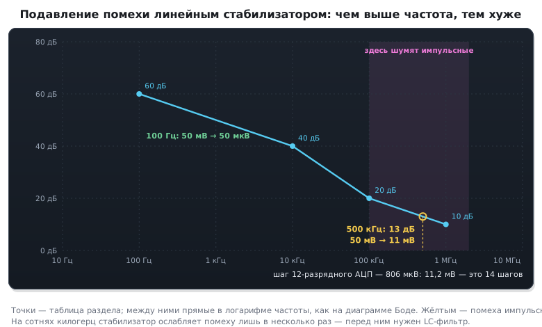
The conclusion: one regulator is not enough for the analog section. You need an LC filter before it (section 53.4), separate decoupling and layout, and sometimes power for the analog section from its own linear regulator connected to the input ahead of the converter.
55.7 The output capacitor: the one nobody writes about
The output capacitor is part of the feedback loop, and stability depends on it. Older-series devices specify an ESR window in the datasheet: for example, from 0.2 to 5 Ω.
- tantalum or electrolytic with 0.5 Ω — inside the window;
- ceramic with 0.01 Ω — below the window, the regulator turns into an oscillator.
The window is narrow — only 25 times, and "improving" the circuit by replacing an old electrolytic with modern ceramics breaks it. The symptom: ripple at the output at hundreds of kilohertz that was not there before.
Modern devices are made stable specifically with ceramics; then the datasheet says "ceramic stable" outright. Always check this, especially when replacing a device with an equivalent.
55.8 Protection
Almost every regulator has two built-in protections: current limiting and thermal shutdown. Reverse input polarity protection is present only in some devices (above all automotive ones); for the rest it is added externally — with a diode or a MOSFET in the supply path.
Current limiting alone does not save it: with the output shorted, a 12 V input and a 1.5 A limit, the device dissipates 18 W. Even with a 5 °C/W heatsink (the whole path 10 °C/W, as in 55.4) that is 220 °C — far beyond the limit. What saves it is precisely thermal shutdown, which turns the device off and back on once it has cooled down.
What is worth adding externally: a diode in parallel (cathode to the input) in case the output ends up higher than the input — for example, at power-off, when the output capacitor is still charged.
55.9 Pitfalls
The board heats up in one spot. Calculate (Vin − Vout) × I and the
junction temperature. Most likely you need a different package or a switching
converter.
Works on the bench, shuts down in the enclosure. The thermal calculation was done for 25 °C instead of the real 60–85.
The output is tenths of a volt below the rating. Not enough input-output headroom.
The output "rings" at hundreds of kilohertz. The output capacitor is outside the ESR window — usually ceramic instead of electrolytic.
The coin cell drains in two days. The quiescent current of a classic regulator.
Noise in the ADC after a switching supply. Rejection at hundreds of kilohertz is only 20 dB.
The adjustable regulator outputs anything it likes with no load. No minimum current: the feedback divider was made too high-impedance.
The device burned out at power-off. The output capacitor ended up charged above the input — a reverse diode is needed.
Replaced with an "identical" equivalent, and everything broke. A different required capacitor, a different dropout, a different pinout — three-pin regulators have no standard pin order.
55.10 Summary
- A linear regulator turns the voltage difference into heat; the input current equals the output current.
- An adjustable one is set by a divider from the 1.25 V reference; the accuracy is determined by the reference (±2 % → 131 mV), not by the resistor series; the divider serves as the minimum load.
- Input-output headroom is decisive with battery power: a classic part does not work from lithium at all; a device with 0.2 V holds 3.3 V up to 85 % of the capacity, one with 50 mV up to 92 %; below the threshold the output simply follows the input.
- The thermal calculation is mandatory and is done for the maximum ambient temperature: 0.255 W in SOT-23 gives 104 °C at 40 °C ambient and no longer passes at 85 °C.
- 3.5 W needs a thermal path no worse than 24.3 °C/W; a switching converter at the same point loses 12.6 times less.
- Quiescent current differs five thousand times: from 1.8 days to 25 years on one coin cell.
- Noise rejection falls with frequency: 50 mV at 500 kHz passes as 11 mV — fourteen ADC steps.
- The output capacitor is part of the loop: ceramic instead of electrolytic turns the regulator into an oscillator.
Next: section 56 "Operational amplifiers" — how to amplify a weak signal to the ADC full scale when there is no built-in amplifier.