 Embedded HandbookApps
22е. LED display drivers TM1637 and MAX7219: a custom two-wire protocol, SPI words, brightness, a cascade of 8×8 matrices
In section 22.3 the microcontroller itself lit the four digits of the display one after another: twelve pins or two 74HC595 chips, a timer interrupt at 1 kHz, transistors on the common pins of the digits. Ready modules spare you all of that: the board carries a driver chip that keeps the scanning, the current and the brightness on its own, and the program only sends it what to show. The most common ones are the TM1637 (four digits on two wires) and the MAX7219 (eight digits or an 8×8 matrix on SPI, the modules are joined into a chain). The first has its own protocol that looks like I²C but is not I²C; the second takes simple 16-bit words, but in a chain it is easy to mix up which word went to whom. Below: both protocols, drivers in C for the STM32F103, the digit table, a chain of four matrices and a scrolling text.
Sources: DocID13587 Rev 17 (STM32F103x8/xB): PA4 is SPI1_NSS, PA5 is
SPI1_SCK, PA7 is SPI1_MOSI, p. 29; PB6 and PB7 are FT, p. 32. The
project has no descriptions of the TM1637 and the MAX7219: the commands,
registers and bit order are taken from the manufacturers' documentation
and are stated in the note at the end. All numbers below come from a run
of the driver _verify/leddrv22g/leddrv22g.c on a computer (gcc 12.2.0)
with our own model of both chips in Python 3.11; the firmware is built by
armclang 6.24 for the Cortex-M3.
What it is called in the documentation
Original Meaning LED driver, display driver driver of an LED display grid, digit digit position segment segment start / stop condition start / stop of a transfer acknowledge (ACK) acknowledgement of reception data command, address command mode command, address command display control, pulse width display control, pulse width (brightness) open drain open drain shift register shift register LOAD (CS) word latch, chip select daisy chain, cascade chain, cascade no-op empty word decode mode, code B decoder mode, digit font B intensity brightness scan limit number of scanned digits shutdown, display test shutdown, display test
22е.1 Why a display driver
Let us compare ways to show four digits:
| Method | MCU pins | Scanning | Digit current |
|---|---|---|---|
| Straight from pins (22.3) | 12 (8 segments and 4 digits) | timer interrupt, 1 kHz | transistors on the digits (22.6) |
| Two 74HC595 (22.1) | 3 (SPI and latch) | timer interrupt, 1 kHz | transistors or switches |
| TM1637 | 2 | the chip itself | the chip itself |
| MAX7219 | 3 (SPI) | the chip itself | the chip itself, a resistor sets the current |
What matters is not the number of pins but that the scanning leaves the program. The display driver walks through the digits and holds the segment current by itself, and the microcontroller writes to it only when the picture changes. A clock that shows minutes talks to the TM1637 once a minute: one write of "12:34" takes 740 µs, and after that the processor does not think about the display. The 1 kHz timer interrupt from section 22.3 and the ghosts of a digit not switched off in time stay in the past.
The choice between them is simple. The TM1637: cheap modules with 4 or 6 digits, often with a colon for clocks; two wires that can be taken from any free pins. The MAX7219: eight digits of eight segments each, that is 64 LEDs per chip: eight digits or an 8×8 matrix. Matrix modules are joined into a chain, and four of them give a screen of 32×8 dots on the same three SPI wires.
22е.2 TM1637: the protocol
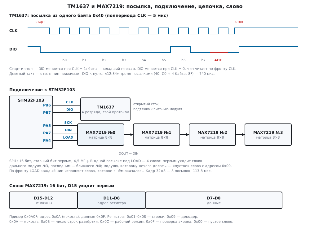
Two lines, CLK and DIO. Both are open drain: both the microcontroller and the chip only pull the line to zero, and the one comes from a pull-up to the supply (section 8.1). A transfer looks like I²C, but there is no device address, and the bits go least significant first:
- start: DIO falls while CLK = 1;
- eight bits: DIO changes while CLK = 0, the chip reads the bit on the rising edge of CLK;
- the ninth clock is the answer: the MCU releases DIO, the chip pulls it to zero (ACK) from the falling edge of the eighth clock to the falling edge of the ninth;
- stop: DIO rises while CLK = 1.
The first byte of a transfer is the command:
| Command | Code | What it does |
|---|---|---|
| data mode | 0x40 |
write, the address grows after each byte |
0x44 |
write to one and the same address | |
| address | 0xC0 + digit 0…5 |
then, in the same transfer, the segment bytes |
| display | 0x80 |
off |
0x88 | brightness 0…7 |
on, 8 brightness steps |
Showing four digits takes three transfers: mode, address with data, display.
uint32_t tm_show(const tm_port_t *p, const uint8_t seg[4], uint8_t bright)
{
    const uint8_t mode = TM_CMD_AUTO;
    const uint8_t data[5] = {TM_CMD_ADDR | 0u, seg[0], seg[1], seg[2], seg[3]};
    uint32_t nack = tm_write(p, &mode, 1);  /* три посылки: режим, адрес с данными, экран */
    nack += tm_write(p, data, 5);
    return nack + tm_bright(p, 1, bright);
}
The model in the test bench takes the bits from the pins and assembles
the transfers. "12:34" at full brightness is 40 | C0 06 DB 4F 66 | 8F:
seven bytes, all with ACK, with a half clock period of 5 µs it takes
740 µs. One digit in fixed-address mode is 44 | C3 6F: a nine into
digit 3, 335 µs, the other digits are not touched. Brightness changes in
one transfer: 88 … 8F are steps 0…7, 87 turns the display off
without erasing the digits.
22е.3 TM1637: code for the F103 and the digit table
CLK on PB6, DIO on PB7, open-drain outputs (MODE = 10, CNF = 01,
in CRL that is 0x66000000). Writing 1 means releasing the line, and the
pull-up raises it; the level can be read through IDR even on an
output, and this is how the driver gets the ACK without switching the pin
to input:
static void tm_clk(uint8_t l) { GPIOB->BSRR = l ? (1u << 6) : (1u << (6 + 16)); }
static void tm_dio(uint8_t l) { GPIOB->BSRR = l ? (1u << 7) : (1u << (7 + 16)); }
static uint8_t tm_dio_in(void) { return (uint8_t)((GPIOB->IDR >> 7) & 1u); }
A byte with the answer, bit-banged, clock period 10 µs:
static uint32_t tm_byte(const tm_port_t *p, uint8_t v)
{
    for (uint32_t i = 0; i < 8u; i++) {
        p->clk(0);
        p->dio((uint8_t)((v >> i) & 1u));   /* младший бит первым; DIO меняется при CLK = 0 */
        p->delay_us(TM_HALF_US);
        p->clk(1);                          /* чип читает бит по фронту CLK */
        p->delay_us(TM_HALF_US);
    }
    p->clk(0);
    p->dio(1);                              /* отпустить DIO: девятый такт — ответ чипа */
    p->delay_us(TM_HALF_US);
    p->clk(1);
    p->delay_us(TM_HALF_US);
    uint32_t nack = p->dio_in();            /* ACK: чип держит DIO в нуле */
    p->clk(0);                              /* по спаду девятого такта чип отпускает DIO */
    p->delay_us(TM_HALF_US);
    return nack;
}
If the module runs from 5 V and its pull-ups go to 5 V, that is fine: PB6 and PB7 of the F103 tolerate 5 V (FT, p. 32), and open drain with such a pull-up does them no harm. The half period of 5 µs is chosen slow and safe; the limiting CLK frequency is in the manufacturer's documentation and was not checked here.
The digit table. Bit 0 is segment a, bit 6 is g, bit 7 is the dot or
the colon: 3F 06 5B 4F 66 6D 7D 07 7F 6F, the same table as in
section 22.3. On clock modules the colon is usually wired to bit 7 of
the second digit, so "12:34" is 06, 5B | 0x80 = DB, 4F, 66;
check it on your module. The model draws what appeared on the display:
"12:34" and all ten digits in three transfers of four:
     _   _
  |  _|: _| |_|
  | |_ : _|   |

 _       _   _
| |   |  _|  _|
|_|   | |_   _|
     _   _   _
|_| |_  |_    |
  |  _| |_|   |
 _   _
|_| |_|
|_|  _|
The bench also checked three mistakes. Bits most significant first,
as is usual on SPI and I²C: the chip receives 02 | 03 B6 BE E0 FE | F1,
not a single command from the table, and the display does not change.
The module is not connected: all 7 bytes without ACK, the driver
returns 7, and the program sees it. DIO is a normal output instead of
open drain: at one the MCU drives the line up while the chip drives it
down during the ACK; the model counted 70 µs of such fighting between
outputs for every write of "12:34", 10 µs per byte.
22е.4 MAX7219: the word, the registers and initialization
Inside the MAX7219 there is a 16-bit shift register. A word goes most significant bit first: D15–D12 do not matter, D11–D8 are the register address, D7–D0 are data. On the rising edge of LOAD (the CS pin on the modules) the chip executes the word that sits in the register.
| Address | Register | Value in the driver |
|---|---|---|
0x00 |
empty word (no-op) | for the chain, 22е.5 |
0x01…0x08 |
digits 0–7 (matrix rows) | the byte is the eight dots of the row |
0x09 |
decoder mode | 0x00, no decoder |
0x0A |
brightness | 0…15 |
0x0B |
number of scanned digits | 0x07, all eight |
0x0C |
shutdown | 0x01, normal mode |
0x0F |
display test | 0x00, off |
For a matrix the decoder is switched off: with it the chip draws a digit
of its font B from the byte, not eight dots. For seven-segment digits the
decoder is handy: a byte 0…9 becomes a digit at once; the order of the
segments in the bits is the MAX7219's own, not as in the table of 22.3,
see the manufacturer's documentation.
Connection: SPI1 as master (section 18): SCK on PA5, MOSI on PA7 to the
DIN input of the module, LOAD on PA4 as a normal pin. 16 bits (DFF = 1),
CPOL = 0, CPHA = 0, prescaler 16: 72 / 16 = 4.5 MHz. MISO is not
needed: the DOUT output of the last module is left unconnected, and PA5,
PA7 without 5 V tolerance (p. 29) receive nothing from the 5 V modules.
Before the rising edge of LOAD the driver waits until SPI has shifted out
the last bit, as with the 74HC595 latch (sections 22.1 and 18.11):
static void max_cs(uint8_t l)
{
    if (l)
        while (SPI1->SR & SPI_SR_BSY)       /* последний бит должен дойти до чипа */
            ;
    GPIOA->BSRR = l ? (1u << 4) : (1u << (4 + 16));
}
Initialization sets all registers explicitly, without relying on their state after power-up, and clears the display while it is still off:
void max_init(const max_port_t *p, uint8_t intensity)
{
    static const uint8_t blank[MAX_N * 8u];
    max_all(p, MAX_TEST, 0x00u);            /* выключить проверку экрана */
    max_all(p, MAX_SCANLIMIT, 0x07u);       /* развёртка всех 8 строк */
    max_all(p, MAX_DECODE, 0x00u);          /* без декодера: байт — это точки */
    max_all(p, MAX_INTENSITY, intensity & 0x0Fu);
    max_frame(p, blank);                    /* стереть, пока экран выключен */
    max_all(p, MAX_SHUTDOWN, 0x01u);        /* рабочий режим */
}
On a chain of four modules that is 13 transfers of 4 words: 52 words,
832 bits, 184.9 µs at SPI 4.5 MHz. The first transfers are 0F00 0F00 0F00 0F00,
0B07 0B07 0B07 0B07, 0900 0900 0900 0900, 0A01 0A01 0A01 0A01.
22е.5 A cascade of four modules: which word goes to whom
The DOUT output of a module is connected to the DIN input of the next one, LOAD is common to all. The chain is four 16-bit registers in a row: each new word enters the near module No. 0 and pushes its previous word into No. 1, that one into No. 2, and so on. On the rising edge of LOAD each chip executes whatever ended up in it. Hence two rules:
- each transfer has exactly as many words as there are modules;
- the word of the far module goes first, the near one last (as with a 74HC595 chain, section 22.1).
To tell something to one module, the others get an empty word with
address 0x00:
void max_one(const max_port_t *p, uint32_t k, uint8_t reg, uint8_t val)
{
    p->cs(0);
    for (uint32_t i = MAX_N; i-- > 0u;)     /* первым уходит слово дальнего модуля */
        p->spi16(i == k ? (uint16_t)((reg << 8) | val) : (uint16_t)(MAX_NOOP << 8));
    p->cs(1);
}
Brightness 15 for module No. 2 alone is the words 0000 0A0F 0000 0000;
in the model only No. 2 changed its brightness. But if you send one word
0A0F, as if there were one module, it lands in the near No. 0, and modules
No. 1–No. 3 repeat on the LOAD edge what was left in their registers
from the previous transfer, here 0A01. In the model brightness 15 went
to No. 0, not to the one it was meant for. If the previous transfer was a
frame, the far modules redraw someone else's rows.
Scanning. Register 0x0B says how many digits to walk through. The
mistake 0x03 instead of 0x07, and the model shows only the top four
rows of "STM32":
..####.#####.#...#.#####..###...
.#.......#...##.##....#..#...#..
.#.......#...#.#.#...#.......#..
..###....#...#.#.#....#.....#...
................................
................................
................................
................................
22е.6 Scrolling text, brightness and current
We keep the frame in memory as 32 columns of one byte: bit 0 is the top
dot. The 5×7 font is also by columns, 6 columns per character: 5 of dots
and an empty one. Output of a frame is 8 transfers, one per row; each has
four words with the row address 0x01…0x08, module No. 3 first. The
left column of a module is bit 7 (that is how the model has it; module
assemblies differ in orientation, and then the bit order or the module
order is reversed):
void max_frame(const max_port_t *p, const uint8_t fb[MAX_N * 8u])
{
    for (uint32_t r = 0; r < 8u; r++) {
        p->cs(0);
        for (uint32_t k = MAX_N; k-- > 0u;) {
            uint8_t row = 0;
            for (uint32_t c = 0; c < 8u; c++)
                if (fb[k * 8u + c] & (1u << r))
                    row |= (uint8_t)(0x80u >> c);   /* левый столбец модуля — бит 7 */
            p->spi16((uint16_t)(((MAX_DIGIT0 + r) << 8) | row));
        }
        p->cs(1);
    }
}
"STM32" is 30 columns out of 32. The first row goes out as the words
0138 015F 01F4 013D, and the model shows:
..####.#####.#...#.#####..###...
.#.......#...##.##....#..#...#..
.#.......#...#.#.#...#.......#..
..###....#...#.#.#....#.....#...
.....#...#...#...#.....#...#....
.....#...#...#...#.#...#..#.....
.####....#...#...#..###..#####..
................................
Scrolling text is the same frame with a shift: the text is drawn from
position x0, and on each step x0 decreases by 1.
void txt_render(uint8_t fb[MAX_N * 8u], const char *s, int32_t x0)
{
    int32_t w = (int32_t)txt_width(s);
    for (int32_t x = 0; x < (int32_t)(MAX_N * 8u); x++) {
        int32_t t = x - x0;                 /* столбец текста под столбцом x экрана */
        fb[x] = (t >= 0 && t < w && t % 6 < 5) ? glyph(s[t / 6])[t % 6] : 0u;
    }
}
STM32F103, 54 columns wide, enters from the right and leaves to the
left in 86 steps (32 + 54). A frame is 512 bits, 113.8 µs at SPI
4.5 MHz; the whole pass is 2752 words and 9784.9 µs of transfer. With a
step of 50 ms a pass lasts 4.3 s, and SPI takes less than 0.3 % of it.
The frame at the step where F103 is on the display:
#####...#....###..#####.........
#......##...#...#....#..........
#.......#...#..##...#...........
####....#...#.#.#....#..........
#.......#...##..#.....#.........
#.......#...#...#.#...#.........
#......###...###...###..........
................................
Brightness. Both chips dim the LEDs with pulses: the TM1637 has 8
steps in the display command, the MAX7219 has 16 steps in register 0x0A.
The steps are uneven to the eye: the difference between the lower steps
is more visible than between the upper ones, as with LED PWM (section 82.2).
Current. In the MAX7219 the peak segment current is set by one resistor RSET between the ISET pin and the supply; the "current versus resistance" table is in the manufacturer's documentation and was not checked here. The digit current at any moment is up to eight segments at once. An example assuming 20 mA per segment: a module with a fully lit matrix draws up to 160 mA, four modules draw 640 mA from 5 V. Work out this current before connecting the chain to the 5 V pin of a development board, and check an "all lit" picture at full brightness before it becomes a screensaver.
22е.7 Pitfalls
Nothing appears on the TM1637 although the transfers go out. The bits
go most significant first: the chip receives 02, 03, F1 instead of
40, C0, 8F. The TM1637 is least significant first.
The driver sees no ACK with a working module. DIO is set up as an input
without pull-up or as a push-pull output. Open drain and a pull-up are
needed; the level is read from IDR of the same pin.
DIO is push-pull, "but it works". On every ACK the outputs of the MCU and of the chip pull the line in opposite directions: 70 µs per write of "12:34". Use open drain.
Digits with wrong segments or without the colon. The module wiring: the colon is bit 7 of one of the digits, six-digit modules sometimes have the digit order mixed up. Check by lighting one segment at a time.
The wrong module of the chain got the command. The transfer has fewer
words than modules: the word went to the near module, the far ones
repeated old words. Exactly four words under one LOAD, the extra ones 0x00.
The picture is upside down or the modules are swapped. The orientation of matrices differs between assemblies: reverse the bit order in a row or the module order.
Only some of the rows are visible. Register 0x0B is not 0x07.
Font digits instead of dots on the matrix. Decoder 0x09 is on;
for a matrix it is 0x00.
The last module catches garbage. LOAD is raised while SPI is still
shifting out the last word: wait for BSY to clear.
The matrix flickers or does not start from 3.3 V. A MAX7219 module at 5 V may not accept a one of 3.3 V: according to the manufacturer's documentation the input threshold at 5 V is 3.5 V. A buffer with a threshold suited to 3.3 V on the SPI lines.
The board resets when everything is lit. The matrix current: up to 160 mA per module at 20 mA per segment. A separate supply or lower brightness.
22е.8 Summary
- A display driver holds the scanning and the current by itself: the MCU writes only when the picture changes; the TM1637 needs 2 wires, the MAX7219 3 SPI wires.
- TM1637: start and stop while CLK = 1, bits least significant first, ACK on
the ninth clock, open drain. Commands
0x40/0x44,0xC0+ digit,0x88| brightness 0–7. - "12:34" is
40 | C0 06 DB 4F 66 | 8F, 740 µs with a 10 µs clock. - MAX7219: a 16-bit word most significant first, the address in D11–D8; registers
0x09,0x0A,0x0B,0x0C,0x0F, rows0x01…0x08. - Chain: a transfer has as many words as there are modules, the far one first;
the extra ones
0x00. Otherwise the far ones repeat old words. - A 32×8 frame is 8 transfers of 4 words, 512 bits, 113.8 µs at 4.5 MHz;
the scrolling
STM32F103takes 86 steps. - The matrix current is RSET and brightness: at 20 mA per segment four modules draw up to 640 mA.
Full sources
leddrv22g.h — ports, TM1637 commands, MAX7219 registers, font.
/* leddrv22g.h — раздел 22е: драйверы индикаторов TM1637 и MAX7219 без регистров.
 * Ноги и SPI — через функции порта: в прошивке fw22g.c это регистры GPIO и SPI1 STM32F103,
 * в стенде host22g.c — функции, которые кормят модель устройств model22g.py. */
#ifndef LEDDRV22G_H
#define LEDDRV22G_H
#include <stdint.h>

/* ── TM1637: два провода, свой протокол, открытый сток ────────────────── */
typedef struct {
    void (*clk)(uint8_t level);         /* 1 — отпустить линию (подтяжка), 0 — прижать к земле */
    void (*dio)(uint8_t level);
    uint8_t (*dio_in)(void);            /* уровень на линии DIO */
    void (*delay_us)(uint32_t us);
} tm_port_t;

#define TM_HALF_US   5u                 /* полпериода CLK: такт 10 мкс */
#define TM_CMD_AUTO  0x40u              /* запись, адрес растёт сам */
#define TM_CMD_FIXED 0x44u              /* запись в один адрес */
#define TM_CMD_ADDR  0xC0u              /* | адрес разряда 0…5 */
#define TM_CMD_DISP  0x80u              /* | 0x08 — экран включён, | 0…7 — яркость */
#define TM_SEG_COLON 0x80u              /* бит 7 разряда: точка или двоеточие часового модуля */

extern const uint8_t tm_digit[10];      /* сегменты цифр, бит 0 — a … бит 6 — g */
uint32_t tm_write(const tm_port_t *p, const uint8_t *b, uint32_t n);     /* -> сколько байтов без ACK */
uint32_t tm_show(const tm_port_t *p, const uint8_t seg[4], uint8_t bright);
uint32_t tm_put(const tm_port_t *p, uint8_t pos, uint8_t seg);
uint32_t tm_bright(const tm_port_t *p, uint8_t on, uint8_t bright);

/* ── MAX7219: 16-битное слово по SPI, цепочка модулей ─────────────────── */
typedef struct {
    void (*cs)(uint8_t level);          /* LOAD: по фронту каждый чип берёт своё слово */
    void (*spi16)(uint16_t w);          /* слово старшим битом вперёд, вернуться — когда ушло */
} max_port_t;

#define MAX_N         4u                /* модулей 8×8 в цепочке: 32×8 точек */
#define MAX_NOOP      0x00u
#define MAX_DIGIT0    0x01u             /* 0x01…0x08 — разряды (строки матрицы) */
#define MAX_DECODE    0x09u
#define MAX_INTENSITY 0x0Au
#define MAX_SCANLIMIT 0x0Bu
#define MAX_SHUTDOWN  0x0Cu
#define MAX_TEST      0x0Fu

void max_all(const max_port_t *p, uint8_t reg, uint8_t val);                 /* одно и то же — всем */
void max_one(const max_port_t *p, uint32_t k, uint8_t reg, uint8_t val);     /* только модулю k */
void max_init(const max_port_t *p, uint8_t intensity);
void max_frame(const max_port_t *p, const uint8_t fb[MAX_N * 8u]);          /* 32 столбца, бит 0 — верх */

/* ── бегущая строка: шрифт 5×7 по столбцам ────────────────────────────── */
uint32_t txt_width(const char *s);                                          /* 6 столбцов на знак */
void txt_render(uint8_t fb[MAX_N * 8u], const char *s, int32_t x0);        /* текст с x0 столбца экрана */

#endif
leddrv22g.c — drivers without registers: the common part of the firmware and the bench.
/* leddrv22g.c — раздел 22е: TM1637 ногодрыгом и MAX7219 по SPI, бегущая строка (без регистров). */
#include "leddrv22g.h"

/* ══ TM1637 ══════════════════════════════════════════════════════════════ */
const uint8_t tm_digit[10] = {0x3F, 0x06, 0x5B, 0x4F, 0x66, 0x6D, 0x7D, 0x07, 0x7F, 0x6F};

static void tm_start(const tm_port_t *p)
{
    p->dio(1);
    p->clk(1);
    p->delay_us(TM_HALF_US);
    p->dio(0);                              /* старт: DIO падает при CLK = 1 */
    p->delay_us(TM_HALF_US);
}

static void tm_stop(const tm_port_t *p)
{
    p->clk(0);
    p->dio(0);
    p->delay_us(TM_HALF_US);
    p->clk(1);
    p->delay_us(TM_HALF_US);
    p->dio(1);                              /* стоп: DIO растёт при CLK = 1 */
    p->delay_us(TM_HALF_US);
}

static uint32_t tm_byte(const tm_port_t *p, uint8_t v)
{
    for (uint32_t i = 0; i < 8u; i++) {
        p->clk(0);
        p->dio((uint8_t)((v >> i) & 1u));   /* младший бит первым; DIO меняется при CLK = 0 */
        p->delay_us(TM_HALF_US);
        p->clk(1);                          /* чип читает бит по фронту CLK */
        p->delay_us(TM_HALF_US);
    }
    p->clk(0);
    p->dio(1);                              /* отпустить DIO: девятый такт — ответ чипа */
    p->delay_us(TM_HALF_US);
    p->clk(1);
    p->delay_us(TM_HALF_US);
    uint32_t nack = p->dio_in();            /* ACK: чип держит DIO в нуле */
    p->clk(0);                              /* по спаду девятого такта чип отпускает DIO */
    p->delay_us(TM_HALF_US);
    return nack;
}

uint32_t tm_write(const tm_port_t *p, const uint8_t *b, uint32_t n)
{
    uint32_t nack = 0;
    tm_start(p);
    for (uint32_t i = 0; i < n; i++)
        nack += tm_byte(p, b[i]);
    tm_stop(p);
    return nack;
}

uint32_t tm_show(const tm_port_t *p, const uint8_t seg[4], uint8_t bright)
{
    const uint8_t mode = TM_CMD_AUTO;
    const uint8_t data[5] = {TM_CMD_ADDR | 0u, seg[0], seg[1], seg[2], seg[3]};
    uint32_t nack = tm_write(p, &mode, 1);  /* три посылки: режим, адрес с данными, экран */
    nack += tm_write(p, data, 5);
    return nack + tm_bright(p, 1, bright);
}

uint32_t tm_put(const tm_port_t *p, uint8_t pos, uint8_t seg)
{
    const uint8_t mode = TM_CMD_FIXED;
    const uint8_t data[2] = {(uint8_t)(TM_CMD_ADDR | (pos & 7u)), seg};
    uint32_t nack = tm_write(p, &mode, 1);
    return nack + tm_write(p, data, 2);
}

uint32_t tm_bright(const tm_port_t *p, uint8_t on, uint8_t bright)
{
    const uint8_t c = (uint8_t)(TM_CMD_DISP | (on ? 0x08u : 0u) | (bright & 7u));
    return tm_write(p, &c, 1);
}

/* ══ MAX7219 ═════════════════════════════════════════════════════════════ */
void max_all(const max_port_t *p, uint8_t reg, uint8_t val)
{
    p->cs(0);
    for (uint32_t k = 0; k < MAX_N; k++)
        p->spi16((uint16_t)((reg << 8) | val));
    p->cs(1);                               /* фронт LOAD: каждый чип исполняет своё слово */
}

void max_one(const max_port_t *p, uint32_t k, uint8_t reg, uint8_t val)
{
    p->cs(0);
    for (uint32_t i = MAX_N; i-- > 0u;)     /* первым уходит слово дальнего модуля */
        p->spi16(i == k ? (uint16_t)((reg << 8) | val) : (uint16_t)(MAX_NOOP << 8));
    p->cs(1);
}

void max_init(const max_port_t *p, uint8_t intensity)
{
    static const uint8_t blank[MAX_N * 8u];
    max_all(p, MAX_TEST, 0x00u);            /* выключить проверку экрана */
    max_all(p, MAX_SCANLIMIT, 0x07u);       /* развёртка всех 8 строк */
    max_all(p, MAX_DECODE, 0x00u);          /* без декодера: байт — это точки */
    max_all(p, MAX_INTENSITY, intensity & 0x0Fu);
    max_frame(p, blank);                    /* стереть, пока экран выключен */
    max_all(p, MAX_SHUTDOWN, 0x01u);        /* рабочий режим */
}

void max_frame(const max_port_t *p, const uint8_t fb[MAX_N * 8u])
{
    for (uint32_t r = 0; r < 8u; r++) {
        p->cs(0);
        for (uint32_t k = MAX_N; k-- > 0u;) {
            uint8_t row = 0;
            for (uint32_t c = 0; c < 8u; c++)
                if (fb[k * 8u + c] & (1u << r))
                    row |= (uint8_t)(0x80u >> c);   /* левый столбец модуля — бит 7 */
            p->spi16((uint16_t)(((MAX_DIGIT0 + r) << 8) | row));
        }
        p->cs(1);
    }
}

/* ══ шрифт 5×7 по столбцам: бит 0 — верхняя точка ═══════════════════════ */
static const char font_ch[] = " 0123FMST";
static const uint8_t font[][5] = {
    {0x00, 0x00, 0x00, 0x00, 0x00},     /* пробел */
    {0x3E, 0x51, 0x49, 0x45, 0x3E},     /* 0 */
    {0x00, 0x42, 0x7F, 0x40, 0x00},     /* 1 */
    {0x42, 0x61, 0x51, 0x49, 0x46},     /* 2 */
    {0x21, 0x41, 0x45, 0x4B, 0x31},     /* 3 */
    {0x7F, 0x09, 0x09, 0x09, 0x01},     /* F */
    {0x7F, 0x02, 0x0C, 0x02, 0x7F},     /* M */
    {0x46, 0x49, 0x49, 0x49, 0x31},     /* S */
    {0x01, 0x01, 0x7F, 0x01, 0x01},     /* T */
};

static const uint8_t *glyph(char ch)
{
    for (uint32_t i = 0; font_ch[i]; i++)
        if (font_ch[i] == ch)
            return font[i];
    return font[0];                         /* нет в шрифте — пробел */
}

uint32_t txt_width(const char *s)
{
    uint32_t n = 0;
    while (s[n])
        n++;
    return n * 6u;                          /* 5 столбцов знака и 1 пустой */
}

void txt_render(uint8_t fb[MAX_N * 8u], const char *s, int32_t x0)
{
    int32_t w = (int32_t)txt_width(s);
    for (int32_t x = 0; x < (int32_t)(MAX_N * 8u); x++) {
        int32_t t = x - x0;                 /* столбец текста под столбцом x экрана */
        fb[x] = (t >= 0 && t < w && t % 6 < 5) ? glyph(s[t / 6])[t % 6] : 0u;
    }
}
fw22g.c — STM32F103 firmware: the TM1637 on PB6, PB7 and four MAX7219 on SPI1.
/* fw22g.c — раздел 22е: TM1637 и цепочка из четырёх MAX7219 от STM32F103 (BluePill), 72 МГц.
 * TM1637: CLK — PB6, DIO — PB7, выходы с открытым стоком, подтяжка к питанию модуля.
 * MAX7219: SPI1 ведущим, SCK — PA5, MOSI (DIN) — PA7, LOAD (CS) — PA4 обычным выводом; 16 бит, 4,5 МГц.
 * Тактирование до 72 МГц — как в разделе 6 (здесь не повторяется); задержки — по счётчику тактов DWT. */
#include "stm32f10x.h"
#include "leddrv22g.h"

#define CPU_MHZ 72u

static void delay_us(uint32_t us)
{
    uint32_t t0 = DWT->CYCCNT;
    while (DWT->CYCCNT - t0 < us * CPU_MHZ)
        ;
}

/* ── TM1637 на PB6, PB7 ───────────────────────────────────────────────── */
static void tm_clk(uint8_t l) { GPIOB->BSRR = l ? (1u << 6) : (1u << (6 + 16)); }
static void tm_dio(uint8_t l) { GPIOB->BSRR = l ? (1u << 7) : (1u << (7 + 16)); }
static uint8_t tm_dio_in(void) { return (uint8_t)((GPIOB->IDR >> 7) & 1u); }

static const tm_port_t tm = {tm_clk, tm_dio, tm_dio_in, delay_us};

/* ── MAX7219 на SPI1 ──────────────────────────────────────────────────── */
static void max_cs(uint8_t l)
{
    if (l)
        while (SPI1->SR & SPI_SR_BSY)       /* последний бит должен дойти до чипа */
            ;
    GPIOA->BSRR = l ? (1u << 4) : (1u << (4 + 16));
}

static void max_spi16(uint16_t w)
{
    while (!(SPI1->SR & SPI_SR_TXE))
        ;
    SPI1->DR = w;
    while (!(SPI1->SR & SPI_SR_RXNE))
        ;
    (void)SPI1->DR;                         /* MISO не подключён: читаем, чтобы снять RXNE */
}

static const max_port_t mx = {max_cs, max_spi16};

static void port_init(void)
{
    RCC->APB2ENR |= RCC_APB2ENR_IOPAEN | RCC_APB2ENR_IOPBEN | RCC_APB2ENR_SPI1EN;
    GPIOB->BSRR = (1u << 6) | (1u << 7);    /* обе линии отпущены */
    /* PB6, PB7: выход с открытым стоком 2 МГц (MODE = 10, CNF = 01) */
    GPIOB->CRL = (GPIOB->CRL & 0x00FFFFFFu) | 0x66000000u;
    GPIOA->BSRR = 1u << 4;                  /* LOAD в единице */
    /* PA4 — выход 2 МГц; PA5, PA7 — альтернативная функция 50 МГц; PA6 — вход, как после сброса */
    GPIOA->CRL = (GPIOA->CRL & 0x0000FFFFu) | 0xB4B20000u;
    /* ведущий, NSS программный, 16 бит, CPOL = 0, CPHA = 0, делитель 16: 72 / 16 = 4,5 МГц */
    SPI1->CR1 = SPI_CR1_MSTR | SPI_CR1_SSM | SPI_CR1_SSI | SPI_CR1_DFF | SPI_CR1_BR_0 | SPI_CR1_BR_1;
    SPI1->CR1 |= SPI_CR1_SPE;
}

int main(void)
{
    static const char text[] = "STM32F103";
    const uint8_t clock[4] = {tm_digit[1], (uint8_t)(tm_digit[2] | TM_SEG_COLON), tm_digit[3], tm_digit[4]};
    uint8_t fb[MAX_N * 8u];
    CoreDebug->DEMCR |= CoreDebug_DEMCR_TRCENA_Msk;     /* счётчик тактов DWT для задержек */
    DWT->CYCCNT = 0;
    DWT->CTRL |= DWT_CTRL_CYCCNTENA_Msk;
    port_init();
    (void)tm_show(&tm, clock, 7u);                      /* «12:34», полная яркость */
    max_init(&mx, 1u);
    for (;;) {
        int32_t w = (int32_t)txt_width(text);
        for (int32_t x0 = (int32_t)(MAX_N * 8u); x0 > -w; x0--) {   /* въезжает справа, уходит влево */
            txt_render(fb, text, x0);
            max_frame(&mx, fb);
            delay_us(50000u);                           /* шаг 50 мс */
        }
    }
}
Next: section 22ж "IR remote and the NEC protocol: VS1838/TSOP receiver, timer capture, interrupt-driven decoder, repeat and noise".