 Embedded HandbookApps
176. Instrumentation amplifier: three op-amps, common-mode rejection, a path for input bias currents
A bridge, a thermocouple, a shunt in the positive wire — in every case the useful signal is the difference of two voltages, while the voltages themselves can sit anywhere within the supply range. The single op-amp difference circuit from 56.5 is too weak for this: its input resistance is low, and its common-mode rejection depends entirely on the tolerance of four resistors.
The numbers below come from an ngspice model built on the extended op-amp macromodel from section 164.
Terms used in the documentation
Term Meaning instrumentation amplifier an amplifier for a small difference of two voltages, with high input resistance difference amplifier an op-amp stage that subtracts one input from the other common-mode voltage the voltage shared by both inputs common-mode rejection ratio (CMRR) how strongly the common-mode signal is suppressed gain-setting resistor (RG) the resistor that sets the gain reference (REF) pin the pin the output is referred to input bias current return path the route by which input bias currents flow back resistor matching / ratio tolerance how closely the resistors match each other input common-mode range the common-mode voltage range allowed at the input
176.1 The three op-amp circuit
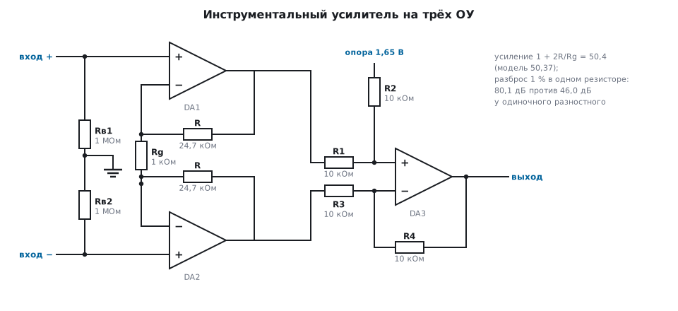
The first stage is two non-inverting amplifiers with a shared resistor between their inverting inputs: the difference is amplified, the common-mode signal passes through with no gain. The second stage is a unity-gain difference amplifier: it subtracts what is left.
The gain of the first stage is 1 + 2R / Rg. In the model R = 24.7 kΩ and
Rg = 1 kΩ, that is 50.4; with a 10 mV difference the model gives
50.37 at the output — the gap comes from the finite gain of the op-amps themselves.
There is only one Rg, and it is external: changing it changes the gain of the whole block, and nothing gets "unbalanced" in the process. This is the main difference from a difference stage, where the gain is set by four resistors at once.
176.2 Common-mode rejection and resistor tolerance
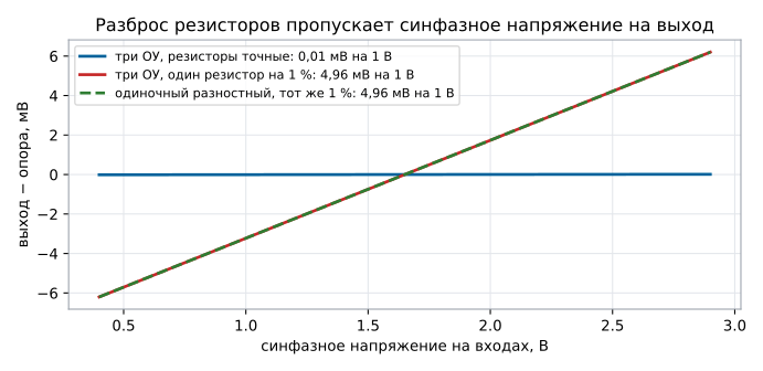
We sweep the common-mode voltage from 0.4 to 2.9 V with a zero difference. Three variants:
| Circuit | Output shift per 1 V of common mode | Common-mode rejection |
|---|---|---|
| three op-amps, exact resistors | 0.01 mV | 134 dB |
| three op-amps, one resistor off by 1 % | 4.96 mV | 80.1 dB |
| single difference stage, gain 1, same 1 % | 4.96 mV | 46.0 dB |
| single difference stage, gain 50, same 1 % | 10.20 mV | 73.7 dB |
The key point: the output shift in the second and third rows is the same, but in the instrumentation amplifier it is divided by the gain of 50.4, while the single difference stage in the third row works at a gain of 1 — hence the difference of 50 times (34 dB). A fair comparison is at equal gain: a difference stage with a gain of 50 and the same 1 % gives 73.7 dB, because its common-mode rejection also grows with gain. The instrumentation amplifier beats it by only about 6 dB. Its real advantages are an input that does not load the source (in the difference stage with a gain of 50 the input is its own 10 kΩ resistors) and a single gain resistor. A ready-made IC with laser-trimmed resistors gives 100…120 dB and needs no selection of parts.
The second consequence: the gain of the difference stage also depends on tolerance. With exact resistors the model gives 50.37, with 1 % in one of the four it gives 50.00, which is a 0.74 % gain error. For the ADC that is 30 codes out of 4096.
176.3 Input bias currents need a path
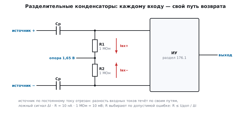
The amplifier inputs draw input bias currents (section 164.1), and these currents have to flow somewhere. If the source is isolated — a thermocouple, an ungrounded strain-gauge bridge, a sensor on a long cable — there is no path, and the inputs drift away.
| Source | Source voltage relative to ground | Output |
|---|---|---|
| isolated, 10 MΩ leakage | −1.96 V | 1.65 V — stuck at the reference |
| the same plus two 1 MΩ resistors to the reference | 1.47 V | 2.154 V — correct |
Without a return path, input bias currents of 100 nA push the source outside the
supply range, the first stage hits a rail, and the output shows the reference instead of the
signal. Two 1 MΩ resistors from each input to the reference (or to ground,
if the signal is unipolar) solve the problem and hardly affect the
measurement: each carries the input bias current plus part of the leakage — in the model 0.17
and 0.18 µA. A difference between the input currents causes no error: the source has a low resistance,
and the difference flows through it — with 100 and 110 nA the output is 2.1535 V versus
2.1537 V. It is different with coupling capacitors at the input: each input has
its own path, and the current difference becomes a false signal ΔI · R:
10 nA · 1 MΩ = 10 mV — the whole signal of the example. In the model with capacitors,
where the source itself is cut off at DC, the output is the same — 2.1535 V.
There R is chosen from the allowed error: R ≤ Uallowed / ΔI.
176.4 The reference and what to connect to it
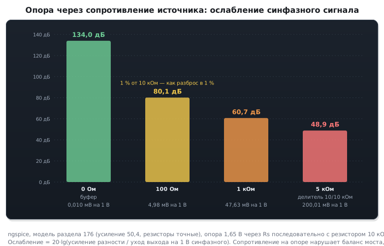
The reference pin sets what the output is measured against: with a single supply it is mid-supply (section 162), when measuring above zero it is ground. An important rule: drive the reference from a low-impedance source — a buffer or a regulator. A two-resistor divider without a buffer ends up in series with a resistor of the difference stage, breaks the matching and destroys the common-mode rejection — exactly like a 1 % tolerance does.
A ready-made instrumentation amplifier IC gives you:
- trimmed resistors and a common-mode rejection of 100…120 dB;
- a single external gain resistor;
- a specified input common-mode range — always check it against the graph in the documentation, especially with a single supply.
176.5 Pitfalls
Bridge readings drift when the supply changes. Weak common-mode rejection: the circuit is a difference stage with a gain of 1 and 1 % resistors — 46 dB.
You built an instrumentation amplifier, but the rejection is still low. The reference is connected to a divider without a buffer, or the second-stage resistors differ.
The output sits at the reference and does not respond to the signal. An isolated source without a return path for the input bias currents.
The gain differs from the calculated value by a fraction of a percent. Tolerance of the second-stage resistors: 1 % in one of them gives 0.74 % of gain.
There is a signal, but at some bridge voltages it disappears. You went outside the input common-mode range — check the graph in the documentation.
176.6 Summary
- A three op-amp instrumentation amplifier: gain
1 + 2R / Rg= 50.4, the model gives 50.37 with a 10 mV difference. - A 1 % tolerance in one resistor: 80.1 dB in the instrumentation amplifier versus 46.0 dB in a single difference stage with a gain of 1 — the difference is exactly the gain of the first stage. At the same gain of 50 the difference stage gives 73.7 dB: the instrumentation amplifier wins by about 6 dB, and above all by an input that does not load the source.
- Exact resistors give 134 dB in the model; the gain error from the same tolerance is 0.74 %.
- An isolated source needs a return path for the input bias currents: without it the source goes to −1.96 V and the output gets stuck at the reference; with two 1 MΩ resistors the output is correct — 2.154 V.
Next: section 176а "4–20 mA current loop: receiving a sensor and driving a PLC input" — how to receive a current-output sensor on the ADC and drive 4–20 mA into a PLC input.