 Embedded HandbookApps
176а. 4–20 mA current loop: receiving a sensor and driving a PLC input
Section 176 showed how to pick up a small voltage difference next to the board. An industrial pressure or temperature sensor usually sits far away — in the workshop, on a pipe, hundreds of meters from the cabinet — and reports its reading not as a voltage but as a current: 4 mA is the start of the scale, 20 mA is the end. This section covers why current is used, how to receive it on the STM32 ADC without burning the input, how much cable a 24 V loop can drive, and how to output 4–20 mA into a PLC input yourself.
Sources: the STM32F103x8/xB datasheet (DocID13587, in the Keil pack it is the file CD00161566.pdf)
and the STM32G474 datasheet (DS12288), reference manual RM0440. All calculations are a
PC model in _verify/loop176a; the voltage-to-current converter is simulated
in ngspice on the op-amp macromodel from section 164; the receive code is built with armclang for
F103 and G474 and run on the PC for every possible window sum. The open-circuit
and short-circuit thresholds (3.6 and 21 mA) are examples: there is no standard with tolerances on disk.
Terms used in the documentation
Term Meaning 4–20 mA current loop a signal carried as a 4–20 mA current live zero the start of the scale is not zero current two-wire (loop-powered) transmitter a sensor powered by the loop itself shunt (burden) resistor the receiver's measuring resistor loop supply, compliance voltage the loop supply; the voltage up to which a source holds its current voltage-to-current converter a circuit that turns a voltage into a current Howland current source a current source built on the Howland circuit injected current (IINJ) current forced into a pin
176а.1 Why current and not voltage
In a series circuit the current is the same at every point. The sensor sets the current, the receiver measures it on its shunt, and the resistance of the wires between them does not enter the result — as long as the supply has enough voltage to push it through (176а.4).
With voltage this does not work. A 0–10 V sensor draws a supply current, and that current returns through the common wire. A 0.5 mm² conductor 200 m long is 7.00 Ω; a supply current of 10 mA (an example) raises the sensor ground on it by 70.0 mV, that is 0.70 % of the 10 V scale. At 1000 m it is 35.00 Ω, 350.0 mV and 3.50 %. Add pickup on top of that: a voltage input has a high resistance, and interference on a long wire goes straight into the signal.
The second advantage is the live zero. The start of the scale is 4 mA, not 0. Zero current does not mean "zero pressure", it means "the loop is broken". The live zero also powers a two-wire sensor: it spends less than 4 mA on its own electronics — the current that flows at the bottom of the scale. The firmware catches two current faults: below 3.6 mA — an open loop or a sensor failure, above 21 mA — a shorted line or a failure (the thresholds here are an example; take them from the sensor datasheet or the customer's requirements).
On top of the loop DC current, the HART protocol transmits digital data by frequency modulation; it is not covered here.
176а.2 The shunt and input protection
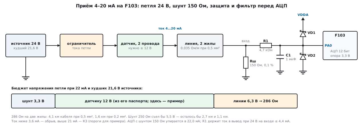
The receiver is a resistor the loop current flows through. The voltage across it is measured by the ADC. The classic 250 Ω shunt gives 1–5 V — but that is not for STM32:
| Shunt | 4 mA | 20 mA | 21 mA | ADC limit | LSB weight | Codes over 4–20 mA |
|---|---|---|---|---|---|---|
| 250 Ω | 1.00 V | 5.00 V | 5.250 V | above the 4.0 V pin limit | — | — |
| 150 Ω, 3.3 V reference (F103) | 0.60 V | 3.00 V | 3.150 V | 22.0 mA | 5.372 µA | 2978 |
| 100 Ω, 2.5 V reference (G474) | 0.40 V | 2.00 V | 2.100 V | 25.0 mA | 6.105 µA | 2621 |
On F103 the voltage limit on a pin that is not 5 V tolerant is 4.0 V (table 6 of the datasheet), and PA0 is exactly such a pin. You can keep the 250 Ω shunt and divide its voltage (section 162), but it is simpler to pick the shunt to match the reference right away: 150 Ω at 3.3 V leaves headroom up to 22.0 mA — the 21 mA short-circuit threshold is still measurable. On G474 with the internal 2.5 V VREFBUF reference, 100 Ω fits.
What the shunt dissipates: at 22 mA it is 72.6 mW. But if the sensor breaks down and 24 V lands directly on the shunt, 160 mA and 3.84 W go through 150 Ω — the resistor burns. That is why the loop has a current limiter: a resettable fuse (section 173) or a transistor limiter.
Between the shunt and the pin there is a resistor R1 and two Schottky diodes: to VDDA and to
ground. The resistor is calculated as in 62.3, for the worst case — 24 V at the input
instead of the signal:
| R1 | Diode current at 24 V | Power in R1 | Error from ±1 µA pin leakage | RC corner with 1 µF |
|---|---|---|---|---|
| 1 kΩ | 20.70 mA — more than 5 mA | 0.428 W | 6.7 µA (0.04 % of scale) | 159.2 Hz |
| 4.7 kΩ | 4.40 mA | 0.091 W | 31.3 µA (0.20 % of scale) | 33.9 Hz |
| 10 kΩ | 2.07 mA | 0.043 W | 66.7 µA (0.42 % of scale) | 15.9 Hz |
The pin injected current limit on F103 is ±5 mA (table 7), the leakage of a regular pin is ±1 µA (table 35). The leakage flows through R1, and the ADC cannot tell its drop from the signal (62.10): the larger the resistor, the larger the error. 4.7 kΩ is the middle ground. The 1 µF capacitor after the resistor is a filter and also a charge reserve for sampling: the sampling capacitance of the F103 ADC is 8 pF.
176а.3 Filter, window and error budget
A long line picks up 50 Hz interference. Let it be 1 mA of amplitude (an example). The 4.7 kΩ / 1 µF RC network passes a fraction of 0.561 at 50 Hz — leaving 560.8 µA, 3.5 % of scale. What saves you is averaging over a window that is a multiple of the mains period:
| Window (samples every 1 ms) | Mains frequency | Residual interference |
|---|---|---|
| 1 | 50 Hz | 560.8 µA (3.505 %) |
| 16 | 50 Hz | 131.7 µA (0.823 %) |
| 20 | 50 Hz | 0.0 µA |
| 20 | 49 Hz | 11.6 µA (0.073 %) |
| 20 | 51 Hz | 10.9 µA (0.068 %) |
Twenty samples every 1 ms are exactly one 50 Hz period, and the interference cancels completely; when the mains drifts by a hertz, less than 0.1 % remains. A window of 16 samples — tempting because you can "divide by shifting" — leaves 0.823 %.
Now the worst case for the static error at 20 mA. A 0.1 % shunt with a TCR of 25 ppm/K, the board heats up by 60 K (an example), resistor R1 is 4.7 kΩ:
| Component, µA at 20 mA | F103: 150 Ω, VDDA reference 3.3 V | G474: 100 Ω, VREFBUF 2.5 V |
|---|---|---|
| Shunt tolerance | 20.0 | 20.0 |
| Shunt TCR | 30.0 | 30.0 |
| Reference tolerance | not counted — it is the supply | 32.0 |
| Reference drift | not counted — it is the supply | 120.0 |
| Total ADC error | 26.9 (±5 LSB) | 48.8 (±8 LSB) |
| of which nonlinearity | 16.1 (±3 LSB) | 26.9 (±4.4 LSB) |
| Pin leakage through R1 | 31.3 (±1 µA) | 4.7 (±100 nA) |
| Before calibration | 108.2 (0.68 % of scale) | 255.5 (1.60 % of scale) |
| After two-point calibration | 77.5 (0.48 %) | 181.6 (1.13 %) |
Numbers from the datasheets: F103 — table 49 (±5 and ±3 LSB) and table 35;
G474 — table 69 (slow channel at full speed, ±8 and ±4.4 LSB),
table 54 (±100 nA), table 78 (VREFBUF 2.496–2.504 V, drift — the drift of
VREFINT plus 50 ppm/°C, with VREFINT up to 50 ppm/°C). A calibration at a single
temperature removes tolerances and offsets, but not drift, not nonlinearity and
not leakage — that changes with heating.
On F103 in LQFP packages the ADC reference is VDDA, and its error goes into the
result one to one: 1 % of supply is 200 µA at 20 mA, more than the whole rest of the
budget. You have to either measure the supply through VREFINT (14.9), or
calibrate it together with the channel. On G474 the main term is the VREFBUF drift:
an external 20 ppm/°C voltage reference would give 24.0 µA instead of 120.0 (section 177).
The model checked two-point calibration (202.3) on a unit with deviations: shunt +0.08 %, reference −0.7 %, ADC offset +3 LSB and a sag of 1.5 LSB in the middle of the scale. Against nominal values this unit is off by 51, 85, 120, 149 and 173 µA at the points 4, 8, 12, 16 and 20 mA. After calibration at 4 and 20 mA it is 0, 4, 8, 7 and 0 µA: only the sag remains.
176а.4 Two-wire sensor: the loop voltage budget
A two-wire sensor is powered by the same loop it regulates. It needs a minimum voltage across its terminals — this is in its datasheet; here we take 12 V (an example). The 24 V supply must push the maximum current through the shunt, the line and the sensor. We calculate at 22 mA — so that the fault current above 21 mA also gets through — and for a 24 V and a 21.6 V (−10 %) supply. Copper is 0.0175 Ω·mm²/m, two conductors, there and back:
| Supply | Shunt | Across the shunt | Left for the line | Line at most | 0.5 mm² cable | 0.2 mm² cable |
|---|---|---|---|---|---|---|
| 24.0 V | 150 Ω | 3.3 V | 8.7 V | 395.5 Ω | 5649 m | 2260 m |
| 24.0 V | 250 Ω | 5.5 V | 6.5 V | 295.5 Ω | 4221 m | 1688 m |
| 21.6 V | 150 Ω | 3.3 V | 6.3 V | 286.4 Ω | 4091 m | 1636 m |
| 21.6 V | 250 Ω | 5.5 V | 4.1 V | 186.4 Ω | 2662 m | 1065 m |
The length is the route length: the resistance of two conductors is 2·0.0175·L / S.
Everything in series in the loop eats into the same margin: a reverse polarity diode
and a limiter (section 173), together 1 V (an example), leave
5.3 V at 21.6 V and 150 Ω, that is 240.9 Ω — 3442 m at 0.5 mm² and 1377 m
at 0.2 mm². A smaller shunt, 150 Ω instead of 250, means not only a 3.3 V ADC
but also 1429 m of extra 0.5 mm² cable at 21.6 V.
If the budget is not enough, the sensor does not fail in an obvious way, it just hits a limit. A 6000 m cable at 0.5 mm² is 420 Ω, and at 21.6 V no current above 16.8 mA gets into the loop: the top of the scale is cut off, and the 21 mA fault signal never arrives.
176а.5 Receive code: window, microamps, open loop
The code is split into two parts. The portable loop_rx.c, without registers, computes
microamps, engineering units and the loop state — it is built both with armclang
for both chips and with gcc on the PC for testing. The register part for F103
takes a sample every 1 ms and accumulates a window of 20 samples.
Parameters and build-time checks:
#define LOOP_N          20u     /* измерений в окне: 20 × 1 мс = ровно период 50 Гц */
#define LOOP_SHUNT_OHM  150u    /* шунт под опору 3,3 В: 20 мА → 3,0 В */
#define LOOP_VREF_MV    3300u   /* у F103 в LQFP опора — это VDDA */
#define LOOP_LO_UA      3600u   /* ниже — обрыв или авария датчика (порог для примера) */
#define LOOP_HI_UA      21000u  /* выше — КЗ линии или авария датчика (порог для примера) */
#define LOOP_DEBOUNCE   3u      /* столько окон подряд до смены состояния: 60 мс */
_Static_assert(LOOP_HI_UA * LOOP_SHUNT_OHM < LOOP_VREF_MV * 1000u,
               "порог КЗ должен лежать ниже предела АЦП: I * R < Vref");
_Static_assert(LOOP_LO_UA < 4000u && LOOP_HI_UA > 20000u, "пороги аварии - вне шкалы 4-20 мА");
_Static_assert(LOOP_N * 4095ull <= 0xFFFFFFFFull, "сумма окна не помещается в 32 бита");
The first check matches the shunt against the reference: the 21 mA short-circuit threshold must lie below the ADC limit. Put a 250 Ω shunt in the header — and the build stops with this message instead of giving you a "saturated" current on the board.
Converting the window sum to microamps is a straight line through two calibration points, in integers with rounding to nearest; engineering units are a second straight line:
int32_t loop_ua(uint32_t sum, const loop_cal_t *c)
{
    int64_t num = ((int64_t)sum - (int64_t)c->s4) * 16000;
    int64_t den = (int64_t)c->s20 - (int64_t)c->s4;
    num += (num >= 0 ? den : -den) / 2;                            /* к ближайшему */
    return 4000 + (int32_t)(num / den);
}

/* микроамперы -> инженерные единицы шкалы lo…hi; вне 4–20 мА — край шкалы */
int32_t loop_eng(int32_t ua, int32_t lo, int32_t hi)
{
    if (ua < 4000) ua = 4000;
    if (ua > 20000) ua = 20000;
    return lo + (int32_t)(((int64_t)(ua - 4000) * (hi - lo) + 8000) / 16000);
}
The diagnostics do not trust a single window: the state changes only if the new one holds for three windows in a row — 60 ms:
loop_state_t loop_diag(loop_diag_t *d, int32_t ua)
{
    loop_state_t now = ua < (int32_t)LOOP_LO_UA ? LOOP_LOW
                     : ua > (int32_t)LOOP_HI_UA ? LOOP_HIGH : LOOP_OK;
    if (now == d->state) {
        d->count = 0;
    } else if (now != d->pending || d->count == 0) {
        d->pending = now;
        d->count = 1;
    } else if (++d->count >= LOOP_DEBOUNCE) {
        d->state = now;
        d->count = 0;
    }
    return d->state;
}
Sampling on F103: the ADC at 12 MHz, a sampling time of 239.5 cycles — one conversion
takes 21 µs, once a millisecond from SysTick:
void SysTick_Handler(void)                  /* раз в 1 мс: одно измерение, 21 мкс */
{
    ADC1->CR2 |= ADC_CR2_ADON;
    while (!(ADC1->SR & ADC_SR_EOC)) { }
    acc += ADC1->DR;
    if (++cnt == LOOP_N) {                  /* 20 мс — окно кратно периоду 50 Гц */
        window_sum = acc;
        acc = 0;
        cnt = 0;
        ready = 1;
    }
}
The PC run (loop_host.c + the same loop_rx.c) went through all 81901 window
sums from 0 to 20 × 4095 and matched the Python model in 81901 out of 81901.
The nominal window sums are 14891 at 4 mA and 74455 at 20 mA; a sum below 13401
gives the "low" state, above 78179 — "high"; the ADC full scale reads as
22000 µA. On a sequence of windows, an open loop (0 mA) was recognized on the third window,
two windows of 22.5 mA in a row were ignored as a spike, three were recognized as a short circuit.
The main rule for the caller: loop_eng clamps the current to the scale, and on an open loop
it returns zero pressure. Check the state first, then the value.
176а.6 4–20 mA output from the MCU
The reverse task — your own device sends a reading to a PLC input. You need a setpoint voltage and a voltage-to-current converter. The simplest one is the current sink from 15.6: the op-amp holds the DAC voltage across a 100 Ω setpoint resistor, the transistor passes that current, and the load is the PLC input between +24 V and the transistor. A 0.4 V setpoint gives 4 mA, 2.0 V gives 20 mA.
The ngspice model at 24 V and a 250 Ω load, setpoint 2.0 V:
| Output stage | Current | Error |
|---|---|---|
| NPN, current gain 50 | 19.61 mA | −1.96 % |
| NPN, gain 100 | 19.80 mA | −0.99 % |
| NPN, gain 300 | 19.93 mA | −0.33 % |
| n-MOSFET | 20.00 mA | — |
| n-MOSFET, op-amp offset 1 mV | 20.01 mA | +10 µA |
The setpoint resistor measures the emitter current, but the collector current goes into the load: the base current is lost. A MOSFET has zero gate current, and what remains is only the op-amp offset — every millivolt across 100 Ω gives 10 µA. The current does not depend on the load: from 1 to 1000 Ω it is the same; at 1100 Ω the MOSFET stage still holds 20.00 mA, at 1200 Ω only 18.46 mA: 24 V is not enough.
A sink works when the PLC input is not tied to the ground of our board. If the PLC input is grounded at one end, you need a current source into a grounded load — the improved Howland circuit (four 10 kΩ resistors and a 100 Ω current sense resistor) — or isolation (section 54). The Howland circuit is sensitive to resistor matching:
| Resistors | 1 Ω load | 250 Ω | 1000 Ω |
|---|---|---|---|
| exact | 20.00 mA | 20.00 mA | 20.00 mA |
| one 0.1 % higher | 20.01 mA | 20.03 mA | 20.11 mA |
| one 1 % higher | 20.10 mA | 20.35 mA | 21.16 mA |
With a 1 % tolerance the current drifts with the load by more than a milliamp — such a Howland circuit is built only on matched resistor networks.
F103 without a DAC — PWM and RC. F103C8 has no DAC (15.1). PWM at 72 MHz / 4096 is 17578 Hz, a step of 0.806 mV, that is 8.06 µA on 100 Ω; 4 mA is a duty cycle of 12.1 %, 20 mA is 60.6 %. A single 10 kΩ / 1 µF RC network leaves a ripple of 4.69 mV peak-to-peak — 46.9 µA, 0.29 % of scale; two buffered networks with the same values leave no more than 3.62 µV. The price is time: settling to 0.1 % takes 69 ms with one network and 92.3 ms with two. And the PWM swings between ground and the pin supply: the supply error goes into the current one to one.
G474 — DAC and VREFBUF. With a 2.5 V reference and a 100 Ω setpoint resistor the step is 6.11 µA; the codes are 590 for 3.6 mA, 655 for 4 mA, 3276 for 20 mA, 3604 for 22 mA.
#define TX_RSET_OHM  100u                   /* резистор уставки: 2,0 В -> 20 мА */
#define TX_VREF_MV   2500u                  /* VREFBUF, VRS = 01 */
#define TX_MAX_UA    22000u                 /* ток верхней аварии тоже должен пройти */

_Static_assert(TX_MAX_UA * TX_RSET_OHM < TX_VREF_MV * 1000u, "уставка на максимум тока выше опоры ЦАП");

/* код ЦАП для тока: U = I * Rset, код = U * 4095 / Vref, с округлением */
uint32_t tx_code(uint32_t ua)
{
    if (ua > TX_MAX_UA)
        ua = TX_MAX_UA;
    return (uint32_t)(((uint64_t)ua * TX_RSET_OHM * 4095u + TX_VREF_MV * 500u) / (TX_VREF_MV * 1000u));
}
The op-amp "+" input has a high impedance, so the DAC output buffer is off (MODE1 = 010):
the total DAC error without the buffer is ±12 LSB, with the buffer ±30 LSB (table 75).
This does not work for the Howland circuit: its input is a 10 kΩ resistor, and the output
impedance of the unbuffered DAC is 9.6–13.8 kΩ (table 74). VREFBUF at 2.5 V
requires VDDA of at least 2.8 V (table 78), and the VRS field may be changed only while the
buffer is disabled — that is why tx_init writes twice.
Output budget at 20 mA, in µA: unbuffered DAC — 73.3 (with the buffer it would be 183.2), VREFBUF tolerance — 32.0, its drift over 60 K — 120.0, the 0.1 % tolerance of the setpoint resistor — 20.0, its TCR — 30.0, the 1 mV op-amp offset — 10.0. In total 285.3 µA, 1.78 % of scale. A two-point calibration with a milliammeter at the output (202.4) removes everything except drift: 150.0 µA, 0.94 %.
176а.7 Pitfalls
An open loop is shown as zero pressure. loop_eng clamps a current below 4 mA
to the start of the scale — zero current turns into "pressure 0". Before using the value,
always check the loop_diag state.
A 250 Ω shunt on a 3.3 V ADC. At 20 mA it is 5.00 V, above the F103
pin limit of 4.0 V. Pick the shunt to match the reference; the _Static_assert in loop_rx.c
will not let you build a mismatched pair.
A window of 16 samples. A shift instead of a division is convenient, but 16 ms is not a mains period: 0.823 % of the interference remains versus zero with a window of 20.
The top of the scale is cut off, and nobody notices. On a long line or with a sagging supply the sensor hits its limit below 20 mA (16.8 mA at 6 km) — the reading looks plausible. Calculate the loop budget for the worst supply, at 22 mA and with all series elements.
The shunt burned together with the sensor. A broken-down sensor puts 24 V on the shunt: 160 mA and 3.84 W through 150 Ω. Without a current limiter in the loop this is what happens.
The Schottky diode pulls VDDA up. With 24 V at the input, 4.40 mA flow through the 4.7 kΩ R1 into the
VDDA rail. If the rail itself consumes less, its voltage
rises — and on F103 that is the reference, so all channels shift. Use a Zener diode or a
clamp on the rail, or a diode to a separate rail.
The loop ground is connected in two places. The shunt sits in the return wire, and the loop minus is the board ground. If it is also grounded at the sensor or in the cabinet, a stray current flows through ground. Then you need isolation (section 54).
The NPN output delivers too little current. With a gain of 50 you lose 1.96 % — the base current does not go through the load. A MOSFET removes the problem.
A Howland circuit on 1 % resistors. The current depends on the load: 20.10 mA at 1 Ω and 21.16 mA at 1000 Ω. And an unbuffered DAC cannot drive its input — it forms a divider with the 10 kΩ resistor.
176а.8 Summary
- The current is the same throughout the loop: the line resistance does not enter the result, and 0 mA is distinguishable from the 4 mA start of the scale. A voltage signal over 1000 m of common wire would be off by 3.50 %.
- Pick the shunt for the reference: 150 Ω at 3.3 V (0.60–3.00 V, 5.372 µA per code, limit 22.0 mA), 100 Ω at 2.5 V. 250 Ω gives 5.00 V — above 4.0 V.
- Input protection: 4.7 kΩ and two Schottky diodes hold the diode current at 24 V to 4.40 mA against a limit of 5 mA; the price is 31.3 µA of error from leakage.
- A 20 × 1 ms window cancels 50 Hz completely; at 49–51 Hz less than 0.1 % remains; a window of 16 leaves 0.823 %.
- Error budget at 20 mA: F103 — 108.2 µA not counting the
VDDAreference (its 1 % adds another 200), G474 with VREFBUF — 255.5 µA. A two-point calibration removes the tolerances; the drift remains. - Loop budget at 21.6 V, 22 mA and 12 V across the sensor: 286.4 Ω of line — 4091 m of 0.5 mm² cable with a 150 Ω shunt and 2662 m with a 250 Ω shunt.
- Code: window sum → µA → engineering units in integers; diagnostics confirmed over three windows (60 ms); PC run — 81901 out of 81901.
- Output: op-amp + n-MOSFET + 100 Ω gives 20.00 mA up to a 1100 Ω load at 24 V; an NPN with a gain of 50 loses 1.96 %; a Howland circuit with a 1 % tolerance drifts up to 21.16 mA. G474: a step of 6.11 µA, a budget of 285.3 µA before calibration.
Full source code
loop_rx.h — 4–20 mA receive: conversion, engineering units, diagnostics — declarations.
/* 176а: приём 4–20 мА — пересчёт суммы окна в микроамперы, инженерные единицы, диагностика.
 * Без регистров: этот же файл собирается armclang для F103 и G474 и gcc на ПК для проверки. */
#ifndef LOOP_RX_H
#define LOOP_RX_H
#include <stdint.h>

#define LOOP_N          20u     /* измерений в окне: 20 × 1 мс = ровно период 50 Гц */
#define LOOP_SHUNT_OHM  150u    /* шунт под опору 3,3 В: 20 мА → 3,0 В */
#define LOOP_VREF_MV    3300u   /* у F103 в LQFP опора — это VDDA */
#define LOOP_LO_UA      3600u   /* ниже — обрыв или авария датчика (порог для примера) */
#define LOOP_HI_UA      21000u  /* выше — КЗ линии или авария датчика (порог для примера) */
#define LOOP_DEBOUNCE   3u      /* столько окон подряд до смены состояния: 60 мс */

typedef struct { uint32_t s4, s20; } loop_cal_t;          /* суммы окна на 4 и 20 мА */
typedef enum { LOOP_OK, LOOP_LOW, LOOP_HIGH } loop_state_t;
typedef struct { loop_state_t state, pending; uint8_t count; } loop_diag_t;

loop_cal_t   loop_cal_nominal(void);
int32_t      loop_ua(uint32_t sum, const loop_cal_t *c);
int32_t      loop_eng(int32_t ua, int32_t lo, int32_t hi);
loop_state_t loop_diag(loop_diag_t *d, int32_t ua);

#endif
loop_rx.c — 4–20 mA receive — the portable part.
/* 176а: приём 4–20 мА — переносимая часть (см. loop_rx.h) */
#include "loop_rx.h"

_Static_assert(LOOP_HI_UA * LOOP_SHUNT_OHM < LOOP_VREF_MV * 1000u,
               "порог КЗ должен лежать ниже предела АЦП: I * R < Vref");
_Static_assert(LOOP_LO_UA < 4000u && LOOP_HI_UA > 20000u, "пороги аварии - вне шкалы 4-20 мА");
_Static_assert(LOOP_N * 4095ull <= 0xFFFFFFFFull, "сумма окна не помещается в 32 бита");

/* сумма окна для тока ua по номиналам: N * I * R * 4095 / Vref, с округлением */
static uint32_t nominal_sum(uint32_t ua)
{
    uint64_t uv = (uint64_t)ua * LOOP_SHUNT_OHM;                  /* мкА * Ом = мкВ */
    return (uint32_t)((uv * LOOP_N * 4095u + LOOP_VREF_MV * 500u) / (LOOP_VREF_MV * 1000u));
}

loop_cal_t loop_cal_nominal(void)
{
    loop_cal_t c = { nominal_sum(4000u), nominal_sum(20000u) };
    return c;
}

/* сумма окна -> микроамперы по прямой через две точки калибровки (4 и 20 мА) */
int32_t loop_ua(uint32_t sum, const loop_cal_t *c)
{
    int64_t num = ((int64_t)sum - (int64_t)c->s4) * 16000;
    int64_t den = (int64_t)c->s20 - (int64_t)c->s4;
    num += (num >= 0 ? den : -den) / 2;                            /* к ближайшему */
    return 4000 + (int32_t)(num / den);
}

/* микроамперы -> инженерные единицы шкалы lo…hi; вне 4–20 мА — край шкалы */
int32_t loop_eng(int32_t ua, int32_t lo, int32_t hi)
{
    if (ua < 4000) ua = 4000;
    if (ua > 20000) ua = 20000;
    return lo + (int32_t)(((int64_t)(ua - 4000) * (hi - lo) + 8000) / 16000);
}

/* обрыв и КЗ: состояние меняется, только если новое держится LOOP_DEBOUNCE окон подряд */
loop_state_t loop_diag(loop_diag_t *d, int32_t ua)
{
    loop_state_t now = ua < (int32_t)LOOP_LO_UA ? LOOP_LOW
                     : ua > (int32_t)LOOP_HI_UA ? LOOP_HIGH : LOOP_OK;
    if (now == d->state) {
        d->count = 0;
    } else if (now != d->pending || d->count == 0) {
        d->pending = now;
        d->count = 1;
    } else if (++d->count >= LOOP_DEBOUNCE) {
        d->state = now;
        d->count = 0;
    }
    return d->state;
}
loop176a_f1.c — 4–20 mA receive on F103: a 150 Ω shunt, a window of 20 samples.
/* 176а: приём 4–20 мА на F103 — шунт 150 Ом, PA0, окно 20 измерений по 1 мс */
#include "loop_rx.h"

#define LOOP_CH  0u                         /* PA0 = ADC1_IN0 */

static volatile uint32_t acc, window_sum;
static volatile uint8_t cnt, ready;

void loop_adc_init(void)
{
    RCC->CFGR = (RCC->CFGR & ~RCC_CFGR_ADCPRE) | RCC_CFGR_ADCPRE_DIV6;   /* 72 / 6 = 12 МГц */
    RCC->APB2ENR |= RCC_APB2ENR_IOPAEN | RCC_APB2ENR_ADC1EN;
    GPIOA->CRL &= ~(GPIO_CRL_CNF0 | GPIO_CRL_MODE0);   /* PA0 аналоговый */
    ADC1->SMPR2 |= ADC_SMPR2_SMP0;          /* 239,5 такта: вход через 4,7 кОм и 1 мкФ */
    ADC1->SQR3 = LOOP_CH;
    ADC1->CR2 = ADC_CR2_ADON;
    for (volatile uint32_t i = 0; i < 100u; i++) { }   /* tSTAB: до 1 мкс */
    ADC1->CR2 |= ADC_CR2_CAL;               /* калибровка F1 обязательна (14.3) */
    while (ADC1->CR2 & ADC_CR2_CAL) { }
}

void SysTick_Handler(void)                  /* раз в 1 мс: одно измерение, 21 мкс */
{
    ADC1->CR2 |= ADC_CR2_ADON;
    while (!(ADC1->SR & ADC_SR_EOC)) { }
    acc += ADC1->DR;
    if (++cnt == LOOP_N) {                  /* 20 мс — окно кратно периоду 50 Гц */
        window_sum = acc;
        acc = 0;
        cnt = 0;
        ready = 1;
    }
}

/* из главного цикла: 1 — готово новое окно; ток в мкА, давление в сотых бара, состояние */
int loop_poll(const loop_cal_t *cal, loop_diag_t *d, int32_t *ua, int32_t *cbar)
{
    if (!ready)
        return 0;
    ready = 0;
    *ua = loop_ua(window_sum, cal);
    *cbar = loop_eng(*ua, 0, 1000);         /* датчик 0–10 бар */
    loop_diag(d, *ua);
    return 1;
}
loop176a_g4.c — 4–20 mA output on G474: VREFBUF, DAC and a current sink.
/* 176а: выход 4–20 мА на G474 — VREFBUF 2,5 В, DAC1 канал 1 (PA4) без буфера,
 * дальше сток тока: ОУ + n-МОП + резистор уставки (вход «+» ОУ высокоомный) */
#include <stdint.h>

#define TX_RSET_OHM  100u                   /* резистор уставки: 2,0 В -> 20 мА */
#define TX_VREF_MV   2500u                  /* VREFBUF, VRS = 01 */
#define TX_MAX_UA    22000u                 /* ток верхней аварии тоже должен пройти */

_Static_assert(TX_MAX_UA * TX_RSET_OHM < TX_VREF_MV * 1000u, "уставка на максимум тока выше опоры ЦАП");

/* код ЦАП для тока: U = I * Rset, код = U * 4095 / Vref, с округлением */
uint32_t tx_code(uint32_t ua)
{
    if (ua > TX_MAX_UA)
        ua = TX_MAX_UA;
    return (uint32_t)(((uint64_t)ua * TX_RSET_OHM * 4095u + TX_VREF_MV * 500u) / (TX_VREF_MV * 1000u));
}

void tx_init(void)
{
    RCC->APB2ENR |= RCC_APB2ENR_SYSCFGEN;   /* такт SYSCFG + COMP + VREFBUF + OPAMP */
    VREFBUF->CSR = (VREFBUF->CSR & ~(VREFBUF_CSR_VRS | VREFBUF_CSR_HIZ | VREFBUF_CSR_ENVR))
                 | VREFBUF_CSR_VRS_0;       /* VRS = 01: 2,5 В; менять только при ENVR = 0 */
    VREFBUF->CSR |= VREFBUF_CSR_ENVR;
    while (!(VREFBUF->CSR & VREFBUF_CSR_VRR)) { }                      /* 2,5 В на VREF+ */
    RCC->AHB2ENR |= RCC_AHB2ENR_GPIOAEN | RCC_AHB2ENR_DAC1EN;
    GPIOA->MODER |= GPIO_MODER_MODE4;       /* PA4 аналоговый */
    DAC1->MCR = (DAC1->MCR & ~(DAC_MCR_MODE1 | DAC_MCR_HFSEL))
              | DAC_MCR_MODE1_1             /* MODE1 = 010: на вывод, буфер выключен */
              | DAC_MCR_HFSEL_1;            /* HCLK 170 МГц > 160 */
    DAC1->DHR12R1 = tx_code(3600u);         /* пока нет данных — ток нижней аварии */
    DAC1->CR |= DAC_CR_EN1;
}

void tx_set_ua(uint32_t ua)
{
    DAC1->DHR12R1 = tx_code(ua);
}
Next: section 176б "PT100/PT1000 resistance thermometer: ratiometry and 2-, 3- and 4-wire connection" — how to convert the platinum resistance into degrees on the built-in ADC and remove the reference and the wires from the result.