 Embedded HandbookApps
160. Long lines on the board and in wires: characteristic impedance, reflections, termination, the I²C edge
An ESP32 or STM32 pin switches within a few nanoseconds, even if the program toggles it once a second. For such an edge, a trace a few centimeters long or a wire to a sensor is no longer a "conductor" but a line along which the signal travels as a wave and reflects from the end. Hence ringing, false edges on clock inputs, and an I²C bus that works on the bench and fails inside the enclosure.
Here you will find a calculation of a microstrip line on FR-4 (the IPC-2141 formula, microstrip.py) and two
ngspice 39 models in the stm-lab:1 image (_verify/esp160/): reflections in a line with and without termination,
and the edge of an I²C bus through a pull-up resistor. The model numbers are an idealization: real traces,
connectors and chip inputs will give different ones, but the order of magnitude and the conclusions stay the same.
Terms used in the documentation
Term Meaning transmission line a long line: a conductor along which the signal travels as a wave characteristic impedance (Z0) the wave impedance of the line propagation delay the time the signal takes to travel along the line reflection, ringing, overshoot a wave bounced back, oscillation, a spike above the level series / parallel termination matching with a resistor at the source / at the end microstrip a microstrip line: a trace over a solid ground plane effective permittivity the permittivity the wave actually sees rise time how long the edge takes to rise pull-up resistor, bus capacitance a resistor to the supply, the capacitance of the bus
160.1 When a trace becomes a line
A signal on a trace over a ground plane travels slower than in vacuum: part of the field passes through the fiberglass. For a 50 Ω line on 1.5 mm FR-4 the effective permittivity is 3.385, the speed is 162.9 mm/ns, and the delay is 6.14 ps per millimeter.
A line is considered long when its propagation delay is greater than roughly a sixth of the edge. With a 1 ns edge that is 27 mm of trace, with 5 ns — 136 mm, with 10 ns — 272 mm. The edge of a microcontroller pin is a few nanoseconds, so a half-meter wire to a sensor is always a long line, and a trace on the board becomes one from a few centimeters.
160.2 Characteristic impedance of a microstrip
A trace over a solid ground plane is a microstrip. Its characteristic impedance depends on
the trace width w, the dielectric thickness h and the permittivity, not on the length. The IPC-2141 formula for
FR-4 with 35 µm copper:
| Thickness to ground | Trace width | Z0 |
|---|---|---|
| 1.5 mm | 0.3 mm | 124.7 Ω |
| 1.5 mm | 1.0 mm | 85.0 Ω |
| 1.5 mm | 2.729 mm | 50 Ω |
| 0.2 mm | 0.326 mm | 50 Ω |
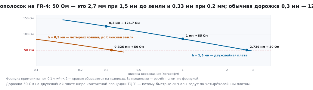
On a 1.5 mm two-layer board a 50 Ω trace is almost 3 mm wide — that is an antenna feed line, not a signal line. A narrower option is the coplanar line: a trace with a gap to the ground pour on both sides, ground underneath, rows of vias along it. On the same 1.5 mm board a 1.2 mm trace with a 0.2 mm gap gives about 50 Ω — this is how the ESP32 antenna pin is routed to the connector. For many signal lines a pour with gaps is inconvenient, so boards with fast signals are made with four layers: the nearest ground layer is 0.2 mm away, and 50 Ω is reached at a width of 0.326 mm. An ordinary signal trace of 0.3 mm on a two-layer board is about 125 Ω, and you have to terminate it for an impedance you do not know exactly.
160.3 Reflections: a line without termination
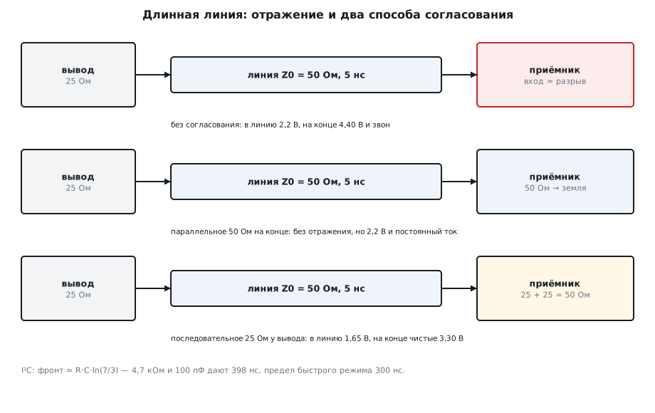
The model: a pin with a 25 Ω output resistance drives a 3.3 V edge with a 1 ns rise into a 50 Ω line with a 5 ns delay (about 80 cm of trace); at the end is a chip input, almost an open circuit. Three variants:
case=1 vmax_end=4.39972 vfinal=3.42208 vmax_near=2.19997
case=2 vmax_end=2.19997 vfinal=2.19997 vmax_near=2.19997
case=3 vmax_end=3.29983 vfinal=3.29983 vmax_near=1.64998
Without termination (case=1) a wave of 3.3 × 50 / 75 = 2.2 V enters the line — a divider formed by the output
resistance and the characteristic impedance. At the open end it reflects completely and doubles: at the receiver
input there are 4.40 V with a 3.3 V supply. The reflection travels back to the source, reflects again
from the unmatched 25 Ω — and the line rings: after 29 ns the end still sits at 3.42 V. On a 3.3 V input
such an overshoot drives current into the supply through the protection diodes, and ringing around the threshold produces extra edges.
160.4 Termination: parallel and series
- Parallel — a 50 Ω resistor at the end of the line (
case=2). There is no reflection, the receiver sees exactly 2.2 V — but that is exactly the trouble. In the high state the 25 + 50 Ω divider draws 3.3 / 75 = 44 mA — more than a pin is allowed (40 mA on the ESP32 at the maximum drive strength, section 153.2; 20–25 mA on the STM32, section 62), and 2.2 V is below the high threshold: 2.475 V on the ESP32 and 2.31 V on the STM32 (section 59.4). This is not how you terminate a microcontroller pin; if the reflection at the end still has to be suppressed, the 50 Ω is placed in series with a capacitor — on an edge the network terminates the line, and there is no DC current. Parallel termination as such is for lines with differential receivers and buses like RS-485, where the resistors at the ends are part of the standard. - Series — a resistor at the source, so that together with the pin's output it adds up to
the characteristic impedance: 25 + 25 = 50 Ω (
case=3). Half goes into the line — 1.65 V; at the open end it doubles to exactly 3.30 V and is not reflected further: the source is matched. There is no DC current, and there is only one resistor. For clock signals and SPI from a microcontroller this is the usual solution: a small resistor right at the pin, chosen so that together with the pin's output resistance it gives the characteristic impedance of the line.
Series termination works only for a single receiver at the end of the line: in the middle of the line the level stays at half for some time.
160.5 I²C: the edge is set by the resistor and the capacitance
I²C has no sharp rising edge: the open-drain output releases the line, and it is pulled up by the pull-up resistor, which charges the capacitance of the wires and inputs. The rise time from 30 to 70 % — the way the I²C specification measures it:
| Bus capacitance | 1.5 kΩ | 4.7 kΩ | 10 kΩ |
|---|---|---|---|
| 100 pF | 127 ns | 398 ns | 848 ns |
| 400 pF | 508 ns | 1593 ns | 3389 ns |
The time grows in exact proportion to R·C: 4.7 kΩ × 100 pF = 470 ns, and the 398 ns edge is 470 × ln(7/3). The edge limit is 1000 ns for standard mode and 300 ns for fast mode (section 17). Hence the picture:
- 4.7 kΩ and 100 pF — standard mode passes with a margin, fast mode (300 ns) no longer does;
- fast mode at 100 pF passes with a pull-up of up to 3.5 kΩ — 300 ns / (0.847 · 100 pF); for example, 2.2 kΩ gives 186 ns;
- at 400 pF — the bus capacitance limit — with 10 kΩ not even standard mode passes.
Every meter of wire and every device adds capacitance. A long I²C bus is not fixed by "lowering the resistor as far as it goes": the output has a current limit in the low state — per the I²C specification it must hold 0.4 V at 3 mA, hence R ≥ (3.3 − 0.4) / 3 mA ≈ 0.97 kΩ, and the pull-up is not taken below about 1 kΩ (section 17). For meters of wire you use I²C bus buffers or a different interface.
160.6 Pitfalls
| Symptom | Cause |
|---|---|
| a clock input catches extra edges | the ringing of an unterminated line crosses the threshold |
| the input sees more than the supply, the chip gets hot | the reflection at the open end doubles the wave |
| with a parallel 50 Ω resistor at the end the logic cannot read a high | a divider with the pin's output resistance: the level is below the threshold |
| a series resistor, and a receiver in the middle of the line fails | in the middle of the line the level stays at half for some time |
| I²C works on the bench, fails in the enclosure on wires | the wire capacitance stretches the edge past the mode's limit |
| fast-mode I²C does not work with modules that have 10 kΩ | with such pull-ups the edge is several times longer than 300 ns |
| a "50 Ω" trace 0.3 mm wide on a two-layer board | with 1.5 mm to ground it is about 125 Ω |
160.7 Summary
- FR-4, 1.5 mm: effective permittivity 3.385, 6.14 ps/mm; with a 1 ns edge a line is long from 27 mm.
- A 50 Ω microstrip: 2.729 mm over 1.5 mm of dielectric, 0.326 mm over 0.2 mm; a 0.3 mm trace over 1.5 mm is 124.7 Ω.
- Without termination: a 2.2 V wave doubles to 4.40 V at the end and rings.
- Parallel 50 Ω — no reflections, but 2.2 V and a DC current; series 25 Ω — 1.65 V into the line and a clean 3.30 V at the end.
- I²C: edge ≈ R·C·ln(7/3); at 100 pF — 127 / 398 / 848 ns for 1.5 / 4.7 / 10 kΩ; the limit is 1000 ns for standard and 300 ns for fast mode; fast mode at 100 pF needs a pull-up from 1 to 3.5 kΩ.
Next: section 161 "Power and loads around the ESP32: the regulator, Wi-Fi peaks, switches, relays and spikes".