 Embedded HandbookApps
39б. Errata in practice: how to read the silicon errata list and work around the bugs
Section 39 said the main thing: the errata list (errata sheet) is read before development, not after the third hour of debugging. Section 39а showed where the official documents are. Here we take the list itself in hand: how to find out the revision of your chip, how to read the summary table and an individual item, which workarounds go into the code and how to keep them so that a year later it is clear where a strange line came from.
Sources: the errata lists ES0182 Rev 13 (F405/407/415/417) and ES0206 Rev 18 (F427/429/437/439), the reference manuals RM0090 and RM0033, all from the Keil packs; the F4 headers and HAL from the pack. The summary tables were parsed by our own model on the PC, the workarounds were built with armclang for the F407.
Terms used in the documentation
Term Meaning errata sheet the list of silicon bugs device limitation a limitation (bug) of the device silicon revision the revision of the silicon revision code marked on device the revision code in the package marking REV_ID, DEV_ID the revision code and the device code in DBGMCU_IDCODE workaround a way around the bug partial workaround a partial workaround: less often, or not in all modes documentation limitation a mistake in the documentation, not in the silicon
39б.1 Where the list is
On this machine the errata lists are in the Keil packs, in the Documentation folder,
under numbers like DM000xxxxx.pdf, so you cannot guess from the file name. The model
opened the first page of every PDF in the STM32 packs and found 19 errata lists:
one in the F2 pack, 14 in the F3 pack and 4 in the F4 pack. For the F407 it is DM00037591.pdf,
which is ES0182 Rev 13 of 45 pages; for the F429, DM00068628.pdf, ES0206 Rev 18
of 54 pages.
The F1 pack has no errata list: it holds sixteen PDFs, datasheets, reference
manuals and the core manual. The F1 HAL from the STM32Cube archive only
refers to it: the comment to HAL_GetREVID() says that on the
F103x8/xB and a number of other F1 devices the registers DBGMCU_IDCODE and DBGMCU_CR are accessible
only under a debugger, "Refer to errata sheet". The F1 errata list itself is downloaded from the
product page (section 39а).
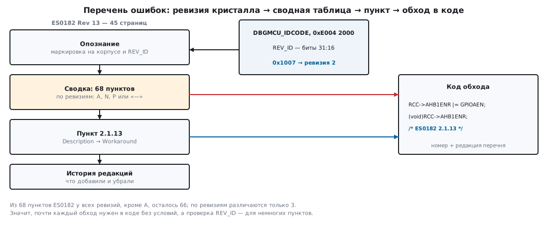
The list consists of four parts: device identification, the summary table, the items one by one, and the revision history.
39б.2 Which revision do I have
The first page of the list tells you how to find out the revision: by the code under the order
number on the package or by the REV_ID field, bits 31:16 of the register
DBGMCU_IDCODE at address 0xE004 2000. The code table is in the reference
manual; for the F4 it is RM0090, section 38.6.1:
| REV_ID | F405/407 | F42x/F43x |
|---|---|---|
| 0x1000 | A | A |
| 0x1001 | Z | — |
| 0x1003 | 1 | Y |
| 0x1007 | 2 | 1 |
| 0x100F | Y and 4 | — |
| 0x101F | 5 and 6 | — |
| 0x2001 | — | 3 |
| 0x2003 | — | 5 and B |
The device code DEV_ID (bits 11:0) is 0x413 on the F405/407 and 0x419 on the F42x.
The documents disagree on a detail: for code 0x2003 RM0090 says "5 and B", while
table 2 of ES0206 itself says "4, 5 and B". When choosing workarounds, trust the errata list:
it is newer and is written precisely about the bugs.
A catch that the list describes itself is item 2.1.2 of ES0182. In revision A
the device code is the same as on the F2, and REV_ID reads 0x2000 instead of
0x1000. According to RM0033, the word 0x2000 0411 is an F205/207 of revision B. The workaround from the
list: tell them apart by the core; the F2 has a Cortex-M3, the F4 a Cortex-M4 (the core part number
in SCB->CPUID is 0xC23 and 0xC24, section 2а):
    if (dev == DEV_F2 && rev == 0x2000u && part == PART_M4)
        return REV_A;                                   /* ES0182 2.1.2 */
    if (dev != DEV_F405_407)
        return REV_UNKNOWN;
The model repeats this function: 0x1007 6413 is an F405/407 of revision 2; 0x2000 0411 with core 0xC24 is revision A, and with core 0xC23 an F2 of revision B; 0x1008 6413 is a code missing from the table, and the function honestly answers "unknown".
39б.3 The summary table: what is fixed
The summary is an "item × revision" table. The marks in ES0182: A means a workaround exists, N means no workaround, P means a partial workaround, a dash means fixed. Newer errata lists, such as ES0206, add D for a documentation error, and a dash means "this revision does not have the bug".
The model parsed table 4 of ES0182 in full: 68 items in 15 groups (system 17, USART 9, I²C and SDIO 6 each, the rest fewer), plus two bugs of the Cortex-M4 core itself in section 1:
| Revision | A: workaround exists | N: no workaround | P: partial | no bug |
|---|---|---|---|---|
| A | 52 | 14 | 1 | 1 |
| 1, 2, 4, 5, 6, Y, Z | 51 | 14 | 1 | 2 |
The main conclusion: over more than nine years of revisions (the first in September 2011, the thirteenth in January 2021) the later silicon revisions fixed two items out of 68. Only three rows differ between revisions: 2.1.1 (flash prefetch in A), 2.1.2 (device code in A) and 2.1.7 (the PDR_ON pin in Z and later, the opposite case: the bug appeared). Almost everything else is the behavior of the silicon forever.
For the F42x the picture is livelier: table 3 of ES0206 has 85 rows, revision A has 84 marked, the latest (4, 5 and B) has 74; eleven items of revision A are fixed in the latest, and one (2.3.10, a missed burst write to PSRAM) appeared from revision 1. The list itself is not free of errors: number 2.10.2 appears in the summary twice.
39б.4 How an item is built
Each item is a title and two paragraphs: Description (what happens and under which conditions) and Workaround (what to do). Read the conditions carefully: they narrow the trouble. Item 2.5.3 of ES0182, a violation of the repeated START timing in I²C, occurs only in master mode, in standard mode from 88 to 100 kHz; the workaround is to go down to 88 kHz or switch to fast mode. Item 2.5.5 covers I²C edges with a 5 V bus: at VDD 3.3 V the bus voltage is at most (VDD + 0.3) / 0.7 = 5.14 V.
A complete example is item 2.1.13 "Delay after an RCC peripheral clock enabling".
Description: after the clock enable bit is written, the block does not come alive at once, but after
2 AHB cycles for blocks on AHB and after 1 + (AHB/APB prescaler) cycles for blocks
on APB. There are three workarounds: a DSB instruction, n NOP instructions, or a dummy read of the same
register. The F4 HAL chose the third and wrote it into every clock enable
macro, with the same title in the comment:
#define __HAL_RCC_GPIOA_CLK_ENABLE()   do { \
                                        __IO uint32_t tmpreg = 0x00U; \
                                        SET_BIT(RCC->AHB1ENR, RCC_AHB1ENR_GPIOAEN);\
                                        /* Delay after an RCC peripheral clock enabling */ \
                                        tmpreg = READ_BIT(RCC->AHB1ENR, RCC_AHB1ENR_GPIOAEN);\
                                        UNUSED(tmpreg); \
                                          } while(0U)
In the F4 HAL headers from the pack this line occurs 243 times. This is what a workaround written by the rules looks like: the code is next to the reason, and the reason is the title of the item.
39б.5 Six workarounds in code
The file errata39c.c collects workarounds from ES0182 for the F407, each with the item number
and the revision of the list. All of them are unconditional: according to the summary these bugs exist
in all revisions.
2.1.13: a pause after enabling the clock. Your own enabling without HAL is a write and a dummy read:
void gpioa_clock_on(void)
{
    RCC->AHB1ENR |= RCC_AHB1ENR_GPIOAEN;
    (void)RCC->AHB1ENR;                                 /* ES0182 2.1.13 */
}
The compiler did not drop the read: the register is declared volatile. The armclang
disassembly: the write, then that very read:
gpioa_clock_on:  MOV   r0,#0x3830
                 MOVT  r0,#0x4002
                 LDR   r1,[r0,#0]
                 ORR   r1,r1,#1
                 STR   r1,[r0,#0]
                 LDR   r0,[r0,#0]
                 BX    lr
2.1.17: removing the backup domain protection. After writing the DBP bit, do a
dummy read of PWR_CR. HAL does the same in HAL_PWR_EnableBkUpAccess()
(the variable dummyread).
2.14.1: changing the ADC sequence. If the conversion was started
by software, a write to ADC_SQRx resets the current conversion, and it
does not restart by itself. The workaround is to set SWSTART again:
    ADC1->SQR3 = (ADC1->SQR3 & ~ADC_SQR3_SQ1) | (ch & 0x1Fu);
    ADC1->CR2 |= ADC_CR2_SWSTART;                       /* ES0182 2.14.1 */
When the conversion is triggered by a timer, the bug does not occur: the new sequence starts with the next trigger.
2.15.1 and 2.15.2: stopping the DAC with DMA. The DMAUDR underrun flag does not stop the DMA stream, and clearing DMAEN does not remove a pending request, so an extra one arrives after the DAC restarts. The order from the list:
    if (DAC->SR & DAC_SR_DMAUDR1)                       /* шаг 1: было ли опустошение */
        DAC->SR = DAC_SR_DMAUDR1;
    DAC->CR &= ~DAC_CR_DMAEN1;                          /* шаг 2 */
    s->CR &= ~DMA_SxCR_EN;                              /* шаг 3 */
DMAUDR1 is cleared by writing a one (RM0090, DAC_SR).
2.5.6 and 2.5.2: a spurious I²C bus error. A master may get BERR by mistake; the transfer does not suffer, and the list only says to clear the flag. BERR is cleared by writing a zero. In the handler you must not read SR2 to find out "am I the master": reading SR1 followed by SR2 clears ADDR. Therefore the mode is a flag of your own driver:
void I2C1_ER_IRQHandler(void)
{
    if ((I2C1->SR1 & I2C_SR1_BERR) && i2c1_master)
        I2C1->SR1 = ~I2C_SR1_BERR;                      /* ES0182 2.5.6: BERR сбрасывается записью 0 */
}
If, however, another master put a STOP in the middle of a byte and START no longer gets generated (2.5.2), the workaround is a software reset of the block with the SWRST bit.
1.2: VDIV and VSQRT in a short interrupt. Core erratum 776924: an FPU division
or square root takes 14 cycles, and if during that time an interrupt of one or two instructions
without FPU instructions arrives and finishes, the result is not written. The
workaround is to turn off lazy FPU state saving, the LSPEN bit (bit 30 of FPCCR at address
0xE000EF34), or not to write handlers shorter than three instructions, not counting
the return instruction.
One more workaround is for debugging only: 2.1.3, three NOP after WFI, if
sleep is debugged with prefetch disabled. The disassembly of sleep_debug_safe
is exactly WFI, three NOP and a return.
Not everything is cured by code. Item 2.1.10 (DMA2 corrupts data if it simultaneously serves DCMI, FSMC with an external FIFO, or GPIO output and a block on APB) is solved by the stream allocation at the design stage, and the fourteen items marked N have no workaround at all: they are taken into account when choosing which blocks to use.
39б.6 A condition on the revision and how to keep workarounds
Checking REV_ID is rarely needed: only for the rows where the summary differs between
revisions. On the F407 there is one example, and it collides with another item. Revision A
has no flash prefetch queue (2.1.1, no workaround), while 2.1.15 advises
turning prefetch off for an accurate ADC and keeping the instruction and data caches:
void flash_accel_setup(enum f40x_rev rev, int precise_adc)
{
    uint32_t acr = (FLASH->ACR & FLASH_ACR_LATENCY) | FLASH_ACR_ICEN | FLASH_ACR_DCEN;
    if (rev != REV_A && !precise_adc)
        acr |= FLASH_ACR_PRFTEN;
    FLASH->ACR = acr;
}
Rules that keep workarounds understandable a year later:
- The comment holds the number, the document and the revision.
ES0182 2.1.13, and in the file header "ES0182 Rev 13". A number without a document is useless: the same item about the pause after enabling the clock is 2.1.13 in ES0182 and 2.2.7 in ES0206; the ADC failure on a sequence change is 2.14.1 and 2.4.1. - No condition if the summary is the same. A revision check where the bug exists in all revisions is extra code and an extra chance to make a mistake.
- An unknown revision is not "new, so fixed". The
defaultinf40x_revision()returns "unknown": with a newREV_IDyou first check the latest revision of the list, then decide. - Workarounds are found by searching for one string. All the places are found by
ES0182: when the chip or the list revision changes, they are checked as a list. - Errata lists change. In revision 9 of ES0182 two items were removed with a note that the I²C bug does not apply to the F40x/F41x. A workaround based on an old revision may turn out to be unnecessary, and a new item may appear.
39б.7 Pitfalls
- Looking for a bug that is not in your own list. The famous sticking BUSY flag in I²C is an item of the F1 list. In ES0182 Rev 13 I²C has six items, 2.5.1–2.5.6, and a sticking BUSY is not among them. A workaround from someone else's list is a reason for a new bug.
- Revision A pretends to be an F2. Device code 0x411 and REV_ID 0x2000 are an F205/207 of revision B according to RM0033. Without a core check, F4 firmware will decide it is running on a foreign chip (2.1.2).
- REV_ID was read on an F103 without a debugger. On the F103x8/xB the register
DBGMCU_IDCODEis inaccessible without a debugger, and the program cannot find out its own revision. The revision of such chips is recorded at assembly or incoming inspection. - The workaround was "optimized". The dummy read after enabling the clock looks
superfluous, and it gets deleted "as unnecessary". Without
volatilethe compiler will do it by itself. The comment with the item number protects the line from people,volatilefrom the compiler. - An item number without the revision. A couple of revisions later the number may point to something else, or to nothing.
- Only the Workaround was read. The conditions in the Description often narrow the bug down to one mode (2.5.3 occurs only from 88 to 100 kHz) or, on the contrary, widen it: 2.1.10 also concerns GPIO as a parallel output.
39б.8 Summary
- On this machine there are 19 errata lists in the Keil packs: F2 has 1, F3 14, F4 4; the F1 pack has none. For the F407 it is ES0182 Rev 13, 45 pages.
- The revision comes from the marking or from
REV_IDinDBGMCU_IDCODE(0xE004 2000): 0x1007 on the F405/407 is revision 2. Revision A has the same code as the F2; tell them apart by the core. - ES0182: 68 items plus 2 core bugs; the later revisions fixed two, and three rows differ between revisions. Almost all workarounds are needed unconditionally.
- An item is a Description with conditions and a Workaround; the F4 HAL carries workaround 2.1.13 in 243 header lines.
- Six workarounds in
errata39c.c: a pause after enabling the clock, a dummy read of PWR_CR, a repeated SWSTART, the order of stopping the DAC with DMA, clearing a spurious BERR, turning LSPEN off. - A workaround comment holds the document, the revision and the item number: the same item stands under different numbers in ES0182 and ES0206.
Full sources
errata39c.c: workarounds for the silicon bugs of the STM32F405/407.
/* errata39c.c — раздел 39б: обходы ошибок кристалла STM32F405/407 в коде.
 *
 * Источник — перечень ошибок ES0182 Rev 13 (январь 2021), файл DM00037591.pdf
 * в паке Keil STM32F4xx_DFP 2.17.1. Номер пункта у каждого обхода — по этой
 * редакции; в других перечнях тот же пункт стоит под другим номером.
 *
 * Сборка (проверка раздела):
 *   armclang --target=arm-arm-none-eabi -mcpu=cortex-m4 -mfpu=fpv4-sp-d16 -mfloat-abi=hard
 *            -DSTM32F407xx -include stm32f4xx.h -O2 -Wall -Wextra -c errata39c.c
 */
#include <stdint.h>

/* Адреса и поля — из заголовков пака; разойдутся с документом — сборка остановится. */
_Static_assert(DBGMCU_BASE == 0xE0042000UL, "DBGMCU_IDCODE по адресу 0xE004 2000 (RM0090, 38.6.1)");
_Static_assert(DBGMCU_IDCODE_REV_ID_Pos == 16U, "REV_ID — биты 31:16");
_Static_assert(DBGMCU_IDCODE_DEV_ID_Msk == 0xFFFUL, "DEV_ID — биты 11:0");
_Static_assert(FPU_BASE + 4UL == 0xE000EF34UL, "FPCCR по адресу 0xE000EF34 (ES0182, 1.2)");
_Static_assert(FPU_FPCCR_LSPEN_Pos == 30U, "LSPEN — бит 30 FPCCR (ES0182, 1.2)");

enum f40x_rev { REV_UNKNOWN = 0, REV_A, REV_Z, REV_1, REV_2, REV_Y_4, REV_5_6 };

#define DEV_F405_407 0x413u   /* RM0090, 38.6.1 */
#define DEV_F2       0x411u   /* RM0033: код F205/207 */
#define PART_M4      0xC24u   /* номер ядра в SCB->CPUID */

/* Ревизия кристалла по DBGMCU_IDCODE.
 * ES0182 2.1.2 «MCU device ID is incorrect» (только ревизия A): код устройства — как у F2,
 * REV_ID — 0x2000 вместо 0x1000. Обход из перечня: отличать F4 от F2 по ядру. */
enum f40x_rev f40x_revision(void)
{
    uint32_t id   = DBGMCU->IDCODE;
    uint32_t dev  = id & DBGMCU_IDCODE_DEV_ID_Msk;
    uint32_t rev  = id >> DBGMCU_IDCODE_REV_ID_Pos;
    uint32_t part = (SCB->CPUID & SCB_CPUID_PARTNO_Msk) >> SCB_CPUID_PARTNO_Pos;

    if (dev == DEV_F2 && rev == 0x2000u && part == PART_M4)
        return REV_A;                                   /* ES0182 2.1.2 */
    if (dev != DEV_F405_407)
        return REV_UNKNOWN;
    switch (rev) {                                      /* RM0090, 38.6.1 */
    case 0x1000u: return REV_A;
    case 0x1001u: return REV_Z;
    case 0x1003u: return REV_1;
    case 0x1007u: return REV_2;
    case 0x100Fu: return REV_Y_4;
    case 0x101Fu: return REV_5_6;
    default:      return REV_UNKNOWN;                   /* новая ревизия: сверить с перечнем */
    }
}

/* Флеш: ES0182 2.1.1 «ART Accelerator prefetch queue instruction is not supported» —
 * у ревизии A очереди предвыборки нет (обхода нет, исправлено в Z и 1).
 * ES0182 2.1.15 «Internal noise impacting the ADC accuracy» — для точного АЦП
 * предвыборку выключить, кэши команд и данных оставить. */
void flash_accel_setup(enum f40x_rev rev, int precise_adc)
{
    uint32_t acr = (FLASH->ACR & FLASH_ACR_LATENCY) | FLASH_ACR_ICEN | FLASH_ACR_DCEN;
    if (rev != REV_A && !precise_adc)
        acr |= FLASH_ACR_PRFTEN;
    FLASH->ACR = acr;
}

/* ES0182 2.1.13 «Delay after an RCC peripheral clock enabling»: после включения такта
 * нужна пауза — обход 3 из перечня: холостое чтение того же регистра. */
void gpioa_clock_on(void)
{
    RCC->AHB1ENR |= RCC_AHB1ENR_GPIOAEN;
    (void)RCC->AHB1ENR;                                 /* ES0182 2.1.13 */
}

/* ES0182 2.1.17 «Possible delay in backup domain protection disabling/enabling after
 * programming the DBP bit»: холостое чтение PWR_CR сразу после записи DBP. */
void backup_domain_unlock(void)
{
    RCC->APB1ENR |= RCC_APB1ENR_PWREN;
    (void)RCC->APB1ENR;                                 /* ES0182 2.1.13 */
    PWR->CR |= PWR_CR_DBP;
    (void)PWR->CR;                                      /* ES0182 2.1.17 */
}

/* ES0182 2.14.1 «ADC sequencer modification during conversion»: при запуске программой
 * смена SQRx сбрасывает текущее преобразование, и само оно не перезапускается —
 * взвести SWSTART ещё раз. */
void adc1_set_first_channel(uint32_t ch)
{
    ADC1->SQR3 = (ADC1->SQR3 & ~ADC_SQR3_SQ1) | (ch & 0x1Fu);
    ADC1->CR2 |= ADC_CR2_SWSTART;                       /* ES0182 2.14.1 */
}

/* ES0182 2.15.1 и 2.15.2: DMAUDR поток DMA не останавливает, а DMAEN=0 не снимает
 * запрос — порядок остановки DAC с DMA из перечня. */
void dac1_dma_stop(DMA_Stream_TypeDef *s)
{
    if (DAC->SR & DAC_SR_DMAUDR1)                       /* шаг 1: было ли опустошение */
        DAC->SR = DAC_SR_DMAUDR1;
    DAC->CR &= ~DAC_CR_DMAEN1;                          /* шаг 2 */
    s->CR &= ~DMA_SxCR_EN;                              /* шаг 3 */
    while (s->CR & DMA_SxCR_EN) { }
    /* шаги 4–5: заново настроить DAC, DMA, запуск — в вызывающем коде */
}

/* ES0182 2.5.6 «Spurious Bus Error detection in Master mode»: ведущему — только
 * сбросить BERR, передача идёт дальше.
 * ES0182 2.5.2 «Start cannot be generated after a misplaced Stop»: обход — SWRST.
 * SR2 здесь не читаем: чтение SR1, а за ним SR2 сбрасывает ADDR (RM0090, I2C_SR1),
 * поэтому «ведущий ли мы» — флаг своего драйвера. */
volatile uint8_t i2c1_master;                           /* 1 от START до STOP */

void I2C1_ER_IRQHandler(void)
{
    if ((I2C1->SR1 & I2C_SR1_BERR) && i2c1_master)
        I2C1->SR1 = ~I2C_SR1_BERR;                      /* ES0182 2.5.6: BERR сбрасывается записью 0 */
}

void i2c1_soft_reset(void)                              /* ES0182 2.5.2 */
{
    I2C1->CR1 |= I2C_CR1_SWRST;
    I2C1->CR1 &= ~I2C_CR1_SWRST;
    /* дальше: заново записать CR2, CCR, TRISE и включить PE */
}

/* ES0182 1.2 «VDIV or VSQRT instructions might not complete correctly when very short
 * ISRs are used» (ошибка ядра 776924): обход 1 — выключить ленивое сохранение FPU. */
void fpu_lazy_off(void)
{
    FPU->FPCCR &= ~FPU_FPCCR_LSPEN_Msk;                 /* ES0182 1.2 */
}

/* ES0182 2.1.3 «Debugging Sleep/Stop mode with WFE/WFI entry»: три NOP после WFI. */
void sleep_debug_safe(void)
{
    __WFI();
    __NOP(); __NOP(); __NOP();                          /* ES0182 2.1.3 */
}
Next: section 39в "From a third-party chip's datasheet to a driver: HTS221 from the first page to testing without a board" — how a driver grows out of a sensor datasheet and how to check it without a board.