 Embedded HandbookApps
208а. A device powered from 24 V: industrial supply, input protection and digital inputs
Section 208 took the device across the border of 230 V mains. The second typical supply for a product is a 24 V DC bus in an automation cabinet: a DIN-rail power supply, and from it controllers, sensors, relays, valves. The bus is safe to touch, but hard to live on. It is shared with contactors and solenoids, sensor wires run for tens of metres, terminals are connected while live and the polarity gets mixed up. This section covers what happens on the bus, how to build the device's power input, how to read a 24 V digital input with a 3.3 V microcontroller and how to drive a coil from an output so that the switch survives turning it off.
Foundations: the optocoupler calculation from 54.2 (current transfer ratio 50…600 %, ageing
by half), protection from 173 (a P-channel MOSFET in the positive lead, a TVS clamp),
the high-side switch from 172.2, pin thresholds from the STM32G474 (DS12288) and
STM32F103 (DocID13587) datasheets from the Keil packs. The numbers are ngspice models in the
stm-lab:1 container (revpol24.cir, hotplug.cir, input.cir, coil.cir) and the
calc208a.py calculation; the code was built with armclang for both MCUs and run in a test on
a PC. There are no standards for industrial power supplies and controller inputs on
disk: the 18…30 V below is a calculation frame, the same as in 54.2, not a tolerance
from a standard. The coil, cable and clamp parameters are nominal — they are
typical values for the calculation, not data for a specific part.
Terms used in the documentation
Term Meaning 24 V DC digital input, type 1 / type 3 a 24 V digital input and its types per the controller standard sinking input / sourcing output an input that accepts the sensor's current / an output that supplies current to the load two-wire sensor, off-state leakage a two-wire sensor and its current when switched off current-limited input an input with a current limiter hot plugging connecting while powered LC input filter an input filter made of an inductor and a capacitor inductive load demagnetization dissipating the coil's energy after switch-off vertical counter the counter bits of all inputs stored in adjacent words sensor supply monitoring checking the supply of the sensors
208а.1 The 24 V bus: what happens on it
The voltage wanders. The power supply outputs 24 V, but at the device terminals at the far end of the cabinet, when the supply sags under load and after adjustment it can be both lower and higher. It is convenient to calculate everything in an 18…30 V frame — a span of 12 V. The lower edge is checked against the input thresholds and the regulator headroom, the upper one against resistor heating (54.2) and the gate limit (below, 208а.2).
Neighbours switch off coils. A contactor or valve on the same bus is an
inductance with stored energy. A nominal 24 V, 48 Ω,
0.3 H coil draws 0.5 A, its time constant τ = L/R = 6.25 ms, and its energy
W = L·I²/2 = 37.5 mJ — 833 times more than the relay from 51.2. If the neighbour
breaks it with a contact without a suppression circuit, the voltage heads towards
U = I·√(L/C): with 1 nF of winding and wire capacitance that is 8.7 kV. That
never happens — the air between the contacts breaks down first, and the bus gets
that same burst of nanosecond pulses from 203.3. The neighbour's suppression circuits are
out of our control, so the device input is designed for whatever
reaches it.
Terminals are connected while live. A wire from the bus is plugged into a running cabinet, and the cable with the capacitor at the device input rings: with the bus at 30 V, the input sees more than 50 V (208а.3).
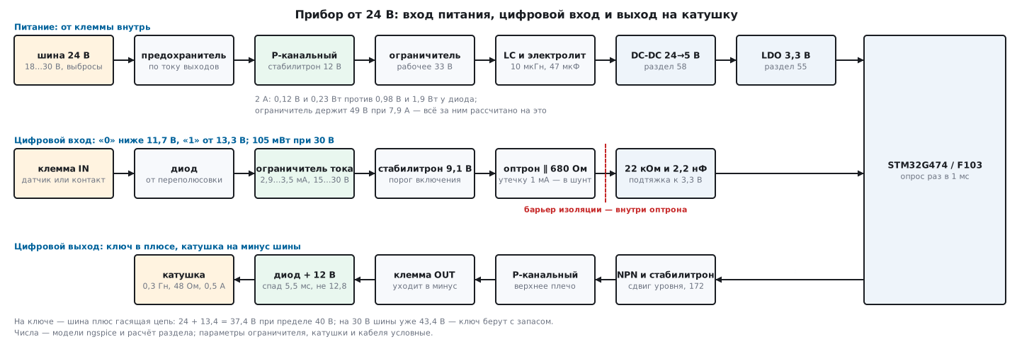
208а.2 Fuse and reverse polarity at two amperes
The first thing after the terminal is a fuse — rated for the current of the device itself, not of the cabinet: the circuit breaker in the cabinet protects the wire, and only its own fuse protects the board. Here the device draws up to 2 A — outputs and logic together. A resettable fuse is convenient, but it trips in hundreds of milliseconds (173.2); the output switches must survive the short-circuit current for at least that time or limit it themselves.
The reverse-polarity protection circuits are the same as in 173.1, but the current is twice as high, and the bus is 24 V. Model: a 12 Ω load, 2 A.
| Circuit | Drop | Loss | Current at −24 V |
|---|---|---|---|
| silicon diode in series | 0.98 V | 1.88 W | 7 nA |
| Schottky diode in series | 0.49 V | 0.95 W | 30 µA |
| P-channel MOSFET in the positive lead | 0.116 V | 0.23 W | 25 pA |
A diode's loss grows as U·I, a transistor's as I²·R: a 58 mΩ channel
at 2 A loses 0.23 W, eight times less than a silicon diode. At two
amperes, almost two watts in one part is noticeable heating, so at such
currents a transistor is chosen.
A gate on 24 V without a Zener will burn out. The gate is pulled to the minus, and the gate-source voltage equals the bus voltage: at the upper edge, 30 V against a typical limit of ±20 V (172.2, 173.1). A 12 V Zener between gate and source with a 100 kΩ resistor holds −11.9 V in the model at both 24 and 30 V; its current is from 60 µA at 18 V to 180 µA at 30 V, its power no more than 2.2 mW. The channel drop at 30 V is 0.145 V: the 12 Ω load already draws 2.5 A.
208а.3 TVS clamp, hot plugging and the filter before the DC-DC
A TVS clamp is chosen by three voltages. The stand-off voltage is above the top of the bus,
otherwise it leaks and heats up all the time: for 30 V, 33 V works, a 3 V margin.
The breakdown voltage is above the stand-off. And under a pulse the voltage on it is the clamping voltage
Uclamp = Ubr + Rd·I (173.3). A nominal clamp — 33 V stand-off,
37 V breakdown, 1.5 Ω dynamic resistance — gives:
| Pulse current | Clamping voltage |
|---|---|
| 7.9 A | 48.9 V |
| 10 A | 52.0 V |
| 20 A | 67.0 V |
Hence the rule: everything behind the clamp — the protection transistor, the electrolytic, the DC-DC input — is chosen with a margin over the clamping voltage, not over the 30 V of the bus. The real numbers are the "clamping voltage at peak pulse current" line in the documentation of the chosen part; they are not here, the numbers are nominal.
Hot plugging. The cable is an inductance (nominally 3 µH and 0.1 Ω,
one to three metres of wire pair), and at the device input there is a 10 µF ceramic. Together this is
a resonant circuit with characteristic impedance Z0 = √(L/C) = 0.55 Ω and
damping ζ = R/(2·Z0) = 0.091 — almost lossless, resonance at 29.1 kHz.
A 30 V step rings it up to U·(1 + e^(−πζ/√(1−ζ²))) = 52.5 V:
75 % overshoot. The hotplug.cir model:
| What is at the input | Input peak | What else |
|---|---|---|
| ceramic 10 µF only | 52.2 V | — |
| ceramic and TVS clamp | 49.3 V | 7.9 A and 3.3 mJ in the clamp |
| ceramic and electrolytic 47 µF, 0.5 Ω | 33.3 V | — |
The clamp barely helps: its 37 V breakdown plus 1.5 Ω · 7.9 A is the
same 49 V. Damping helps: an electrolytic with an internal resistance of
0.5 Ω — of the order of Z0 — damps the ringing down to 33.3 V. So at a 24 V input an electrolytic is placed
next to the ceramic, and its "bad" resistance here is
an advantage.
The filter before the DC-DC. A switching regulator draws current in pulses at
the switching frequency and returns them to the bus — and along the bus they will reach the neighbours.
A 10 µH inductor and a 10 µF capacitor give a resonance at 15.9 kHz and Z0 = 1 Ω;
at a switching frequency of 500 kHz such a filter attenuates the noise by (f/f0)² = 987 times,
by 60 dB. But this is again an LC circuit: at its own resonance it does not attenuate but
amplifies, and the same electrolytic with internal resistance is needed here too.
Layout and inductor choice are in section 58, supply filters in 168.
Why a DC-DC and not a linear regulator. The logic needs 3.3 V at 100 mA. A linear regulator
from 24 V dissipates (Uin − Uout)·I = 2.07 W, from 30 V 2.67 W (thermal
calculation — 55.4). A switching one with a nominal efficiency of 0.85 loses 58 mW and draws
16.2 mA from the bus instead of 100 mA. The usual chain: a 24 → 5 V buck
(58.8), followed by a 3.3 V LDO or a buck straight to 3.3 V.
208а.4 A 24 V digital input: thresholds, current and power
The input is connected to a relay contact, a limit switch or a sensor that puts the bus plus on the terminal. The controller standard divides such inputs into types by thresholds and current; type 3 was invented for two-wire sensors, which pass current through themselves even when off. The standard's tables are not on disk, so the thresholds below are derived from the optocoupler and the circuit, not taken from the standard; check them against it before certification.
The criteria are set by the optocoupler. On the output there is a 22 kΩ pull-up to 3.3 V, that is 0.15 mA. The current transfer ratio is taken per 54.2: a minimum of 50 % halved for ageing, a maximum of 600 %, and another margin of 2 in both directions.
- "1": the LED must get no less than
2 · 0.15 mA / 0.25= 1.2 mA; - "0": no more than
0.15 mA / 2 / 6= 12.5 µA.
The circuit. A reverse-polarity diode, then the element that sets the current, a
9.1 V Zener — it is the threshold: as long as the input is below the sum of the drops across the diode,
Zener and LED, almost no current flows (at 5 V in the model, 6 pA) —
and the optocoupler LED, shunted by a 680 Ω resistor. The current is set either by a
1.5 kΩ resistor or by a two-transistor current limiter: 47 kΩ into the base,
a 200 Ω current-sense resistor, about 0.65 V / 200 Ω. The input.cir model, input sweep
from −31 to +31 V:
| 1.5 kΩ resistor | Current limiter | |
|---|---|---|
| "1" guaranteed from | 14.9 V | 13.3 V |
| "0" guaranteed up to | 12.3 V | 11.7 V |
| input current at 15 V | 2.78 mA | 2.93 mA |
| input current at 24 V | 8.60 mA | 3.33 mA |
| input current at 30 V | 12.5 mA | 3.51 mA |
| LED current at 24 V | 6.91 mA | 1.78 mA |
| power at 24 V | 206 mW | 80 mW |
| power at 30 V | 376 mW | 105 mW |
| current at −30 V | 2.5 nA | 2.5 nA |
Between the two thresholds there is a zone where nothing is guaranteed: the input may show either "0" or "1". This is intentional: a wire with a voltage in the middle is a fault, not a signal.
A resistor is honest, but it heats up. With a resistor the current grows with voltage: at 30 V the circuit dissipates 376 mW, of which 235 mW is in the resistor itself and 117 mW in the Zener. The limiter keeps the current almost constant, and at 30 V the whole circuit takes 105 mW, of which 65 mW is in the transistor (18.5 V across it). On sixteen inputs that is 1.7 W against 6.0 W — a difference you can see in the board temperature in a closed cabinet.
The 680 Ω shunt is against sensor leakage. A switched-off two-wire sensor passes current, 1 mA in the model. It raises the input to 11.5 V (with the resistor, to 11.9 V), but the LED gets 1.0 µA: the whole milliampere goes into the shunt and creates 0.68 V across it, and at that voltage the LED is almost off. Without the shunt, the whole milliampere above the Zener threshold would go into the LED — between the "0" and "1" criteria, so the input could show anything.
208а.5 The MCU side: RC filter and debouncing in firmware
The hardware filter is microseconds. On the MCU pin there is a 22 kΩ pull-up and a
2.2 nF capacitor, τ = R·C = 48.4 µs. The high threshold of the STM32G474 is
0.7·VDD, the low one 0.3·VDD (DS12288); for the STM32F103 they are 0.65·VDD and 0.35·VDD
(DocID13587). When the optocoupler turns off, the pull-up raises the pin to the
high threshold in 58.3 µs on the G474 and 50.8 µs on the F103. When it turns on,
the optocoupler transistor pulls down no less than 1.2 mA · 0.25 = 0.3 mA, of which
0.15 mA goes into the pull-up and 0.15 mA discharges the capacitor: down to the low
threshold in 33.9 µs on the G474 and 31.5 µs on the F103. The nanosecond bursts from 203.3
die here, while contact bounce lasts milliseconds and gets through — it
is removed by the firmware. How to calculate RC on a pin is in 62.7.
The software filter is milliseconds. Sampling once every 1 ms, an input is accepted
as a new level after four identical samples in a row: a 4 ms delay,
a pulse shorter than 4 ms does not pass, the frequency limit is 1/(2 · 4 ms) = 125 Hz.
In 198в.6 this filter is built as one counter per input; here it handles all
sixteen inputs of a port at once, without a loop and without branches. Each input has a
two-bit counter, but the bits are stored "vertically": the low bits of all
sixteen counters are in one word cnt0, the high bits in cnt1. One
operation on a word is one counting step for all inputs at once:
/* Четыре подряд отсчёта, не совпавших с признанным состоянием, — и вход
 * переключается. Все входы разом, без ветвлений. Возвращает переключившиеся. */
uint32_t di_debounce(di_t *d, uint32_t raw)
{
    uint32_t delta  = (raw ^ d->state) & DI_MASK;   /* где отсчёт спорит с состоянием */
    uint32_t toggle = delta & d->cnt0 & d->cnt1;    /* счётчик был на 3 — это 4-й     */
    d->glitch |= (d->cnt0 | d->cnt1) & ~delta;      /* счёт начался и оборвался       */
    d->cnt1 = (d->cnt1 ^ d->cnt0) & delta;          /* +1, а при согласии — сброс     */
    d->cnt0 = ~d->cnt0 & delta;
    d->state ^= toggle;
    return toggle;
}
Where the sample matches the state, delta is zero, and both counter bits
are cleared; where it disagrees, the counter adds one, and on the fourth
disagreeing sample the state bit flips. armclang with -O2
for the G474 turns the function into 20 instructions without a single branch: the
polling time does not depend on what is happening on the inputs.
Diagnostics. Debouncing by itself hides faults: an input that jumps every 10 ms will never switch and will look "just off". So the polling counts raw edges and monitors the sensor supply:
/* Опрос раз в 1 мс: port — чтение порта как есть, supply_ok — питание датчиков
 * в норме (свой вход или АЦП). Без питания входы не признаются — замораживаются. */
uint32_t di_poll(di_t *d, uint32_t port, int supply_ok)
{
    uint32_t raw = (port ^ DI_ACTIVE_LOW) & DI_MASK;
    uint32_t toggle = 0u;
    uint32_t e = raw ^ d->last_raw;                 /* сырые перепады — для диагностики */
    d->last_raw = raw;
    d->supply_ok = (uint8_t)(supply_ok != 0);
    if (d->supply_ok) {
        toggle = di_debounce(d, raw);
    } else {
        d->cnt0 = 0u;                               /* без питания нули — не сигнал   */
        d->cnt1 = 0u;
    }
    for (uint32_t i = 0u; e != 0u; i++, e >>= 1) {
        if ((e & 1u) != 0u && d->edges[i] < UINT16_MAX) {
            d->edges[i]++;
        }
    }
    if (++d->window_ms >= DI_WINDOW_MS) {           /* окно закрыто: итог по дребезгу */
        uint32_t ch = 0u;
        for (uint32_t i = 0u; i < DI_COUNT; i++) {
            if (d->edges[i] > DI_CHATTER_MAX) {
                ch |= 1u << i;
            }
            d->edges[i] = 0u;
        }
        d->chatter = ch;
        d->window_ms = 0u;
    }
    return toggle;
}
More than 20 edges in a 1000 ms window sets the "chattering" flag, and
di_valid_mask() excludes the input from the valid ones. The glitch flag is raised
when counting started and was cut short — there was a disturbance shorter than four samples; it
is sticky, the firmware clears it itself after reading it. If the sensor supply
is lost, all inputs drop to zero at once — this is not a signal but a fault:
the state is frozen, and there are no valid inputs. The thresholds and sizes are checked by
_Static_assert; the port is read with a single instruction — on the G474 at address
0x4800 0410, on the F103 at 0x4001 0C08 (the IDR register is at different
offsets on them, and this is also checked at build time).
The di_test.c test on a PC:
| Experiment | Result |
|---|---|
| clean step at 10 ms | accepted at 13 ms — on the fourth sample |
| bounce at 10…15 ms, then steady | one switch, at 18 ms; glitch flag raised |
| pulses of 1, 2, 3 ms | did not pass; a 4 ms pulse passed |
| 100 Hz square wave (5 ms half-period) | 199 switches in 1 s out of 200 |
| square wave of about 167 Hz (3 ms half-period) | not a single switch |
| input jumps every 10 ms | chatter flag, valid inputs 0xFFF7; cleared after a quiet window |
| sensor supply lost for 50 ms | state 0x00F0 kept, valid 0x0000 |
| 16 steps at 10…25 ms | accepted at 13…28 ms, each on time |
208а.6 A digital output: high-side switch and a coil
In a cabinet the load is usually connected with one end to the bus minus, and the switch is placed in the plus. A load wire shorted to the cabinet body (which is at minus) then does not switch the load on — whereas with the switch in the minus it would: the coil already hangs on the plus. The switch is a P-channel MOSFET with an NPN level shifter from 172.2 and the same 12 V Zener on the gate as in 208а.2. The load is the nominal coil from 208а.1: 0.3 H, 48 Ω, 0.5 A.
When the switch turns off, the coil current keeps flowing and pulls the output terminal
below the minus — exactly as far as needed for a path to appear. Which
path to give it is a choice between speed and the voltage on the switch. The
coil.cir model (a transistor with 40 V breakdown, time from the moment of switch-off):
| Suppression circuit | Output terminal | Decay to 10 % | Where the energy went |
|---|---|---|---|
| none | −16.7 V: switch in breakdown | 4.7 ms | 48.4 mJ into the switch |
| diode | −0.87 V | 12.8 ms | 2.3 mJ into the diode, the rest into the winding |
| diode and 12 V Zener | −13.4 V | 5.5 ms | 17.8 mJ into the suppression circuit |
| diode and 37 V TVS clamp | −16.7 V: switch in breakdown | 4.7 ms | 48.4 mJ into the switch |
A check against the L/R model: the current decays with time constant τ towards "−Uclamp/R", and it reaches
10 % in τ · ln((I0 + Uclamp/R) / (0.1·I0 + Uclamp/R)) — 12.68 ms with
the diode and 5.39 ms with the diode and Zener; down to zero in the second case it takes
τ · ln(1 + I0·R/Uclamp) = 6.42 ms (6.5 ms in the model), and the energy in the suppression
circuit is 17.9 mJ. With a diode alone, a valve or relay releases more than twice
as late, and the contacts separate more slowly (51.2).
The price of speed is the voltage on the switch. The drain-source sees the bus plus
the suppression circuit voltage: 24 + 13.4 = 37.4 V — already tight against a 40 V limit,
and at the upper edge of the bus 30 + 13.4 = 43.4 V — beyond the limit. A 40 V switch
is suitable only with a lower-voltage Zener; otherwise a 60 V switch is used.
A TVS clamp "with margin" is useless. A 37 V clamp in series with the diode does not get a chance to open: the switch breaks down first, at 40 V. The switch takes 48.4 mJ — more than there was in the coil (37.5 mJ): while the switch is in breakdown, the bus keeps pouring current through it. Without a suppression circuit it is the same. Whether the switch survives such a switch-off a thousand times a day is decided by the datasheet avalanche energy, and the model does not know it.
208а.7 Pitfalls
The device burns out when the bus wire is plugged in "on the fly". The ceramic
at the input and the cable inductance ring: a 30 V bus gives 52 V at the input.
A TVS clamp barely helps (49 V), an electrolytic with an internal resistance of
the order of Z0 does (33 V). Input parts need a margin over the peak, not
over 24 V.
An output with a "good" TVS clamp burns at every switch-off. A 37 V clamp together with a 24 V bus requires more than 60 V from the switch, but the switch breaks down at 40 V and takes 48 mJ itself. Add the suppression circuit voltage to the top of the bus and compare with the switch limit.
The valve releases late. A diode alone on the coil holds the current for 12.8 ms instead of 5.5 ms with a diode and Zener. Where release speed matters, add a Zener to the diode — and recalculate the voltage on the switch.
All inputs "switched off" at once. The sensor supply was lost — and the polling honestly sees zeros. Without supply monitoring the firmware will take the fault for a command; with it, the state is frozen and there are no valid inputs.
An input is "on" although the sensor is off. A two-wire sensor in the off state passes about a milliampere — without a shunt across the LED this current goes into the optocoupler and lands between "0" and "1". A 680 Ω shunt leaves the LED 1 µA.
A pulse counter loses pulses. A 4 ms debounce cuts everything shorter than 4 ms and above 125 Hz — a 167 Hz square wave produces not a single switch. To count fast pulses, route the input to a timer (section 13), and keep debouncing for buttons and limit switches.
A linear regulator from 24 V is red-hot. 100 mA down to 3.3 V is 2.07 W at 24 V and 2.67 W at 30 V. From a 24 V bus, power the logic through a buck DC-DC.
208а.8 Summary
- The bus is calculated in an 18…30 V frame; a neighbour's coil (0.3 H, 0.5 A) stores 37.5 mJ — 833 times more than the relay from 51.2 — and without a suppression circuit it sends bursts of pulses into the bus.
- Reverse polarity at 2 A: a diode loses 1.88 W, a P-channel MOSFET 0.23 W; a gate at 24…30 V needs a 12 V Zener (current 60…180 µA).
- TVS clamp: stand-off voltage above 30 V, and everything behind it above the clamping voltage (a nominal 48.9 V at 7.9 A). Hot plugging gives 52.2 V on the ceramic; an electrolytic of 47 µF / 0.5 Ω brings it down to 33.3 V.
- A 10 µH / 10 µF filter attenuates DC-DC noise at 500 kHz by 60 dB; a linear 24 → 3.3 V at 100 mA heats up by 2.07 W against 58 mW for a switching one.
- Digital input: the optocoupler requires 1.2 mA for "1" and no more than 12.5 µA for "0"; a current limiter gives thresholds of 13.3 / 11.7 V and 105 mW at 30 V against 376 mW for a resistor; a 680 Ω shunt reduces a 1 mA sensor leakage to 1 µA in the LED.
- An RC of 22 kΩ / 2.2 nF filters tens of microseconds (58.3 µs to the threshold on the G474); bounce is removed by firmware: 4 samples of 1 ms, pulses shorter than 4 ms rejected, a 125 Hz limit; 16 inputs in 20 instructions without branches.
- Diagnostics are mandatory: chatter (more than 20 edges in 1 s), rejected glitches and the sensor supply — otherwise a fault looks like "input off".
- Output: a high-side switch; a diode gives a 12.8 ms decay, a diode and a 12 V Zener 5.5 ms at the cost of 37.4 V on the switch with a 24 V bus and 43.4 V at 30 V.
Full sources
p24v208a.c — polling 24 V inputs: debouncing with vertical counters and diagnostics.
/* Раздел 208а: опрос дискретных входов 24 В — антидребезг на вертикальных
 * счётчиках и диагностика (дребезг, отвергнутые помехи, питание датчиков).
 * di_poll() вызывается раз в 1 мс; входы — биты 0…DI_COUNT-1 одного порта.
 * Ядро переносимое; чтение порта — только при сборке под STM32G474 или STM32F103. */
#include <stdint.h>
#include <stddef.h>

#define DI_COUNT        16u        /* входов на порту                           */
#define DI_MASK         ((1u << DI_COUNT) - 1u)
#define DI_ACTIVE_LOW   DI_MASK    /* оптрон тянет вывод к нулю: активен нулём  */
#define DI_WINDOW_MS    1000u      /* окно подсчёта перепадов                   */
#define DI_CHATTER_MAX  20u        /* больше перепадов за окно — «дребезжит»    */

_Static_assert(DI_COUNT >= 1u && DI_COUNT <= 16u, "входы — на одном 16-битном порту");
_Static_assert((DI_ACTIVE_LOW & ~DI_MASK) == 0u, "маска инверсии шире числа входов");
_Static_assert(DI_CHATTER_MAX < DI_WINDOW_MS, "порог дребезга больше числа отсчётов в окне");

typedef struct {
    uint32_t state;              /* признанное состояние, 1 = вход активен      */
    uint32_t cnt0, cnt1;         /* два бита счётчика на вход, «вертикально»    */
    uint32_t last_raw;           /* сырой отсчёт прошлого опроса                */
    uint32_t chatter;            /* флаги: за прошлое окно вход дребезжал       */
    uint32_t glitch;             /* флаги: был импульс короче четырёх отсчётов  */
    uint16_t edges[DI_COUNT];    /* сырые перепады в текущем окне               */
    uint16_t window_ms;
    uint8_t  supply_ok;          /* питание датчиков было в норме в этом опросе */
} di_t;

_Static_assert(DI_WINDOW_MS <= UINT16_MAX, "окно и счётчики перепадов — в uint16_t");
_Static_assert(offsetof(di_t, cnt0) == 4u && offsetof(di_t, cnt1) == 8u, "раскладка di_t");

/* Четыре подряд отсчёта, не совпавших с признанным состоянием, — и вход
 * переключается. Все входы разом, без ветвлений. Возвращает переключившиеся. */
uint32_t di_debounce(di_t *d, uint32_t raw)
{
    uint32_t delta  = (raw ^ d->state) & DI_MASK;   /* где отсчёт спорит с состоянием */
    uint32_t toggle = delta & d->cnt0 & d->cnt1;    /* счётчик был на 3 — это 4-й     */
    d->glitch |= (d->cnt0 | d->cnt1) & ~delta;      /* счёт начался и оборвался       */
    d->cnt1 = (d->cnt1 ^ d->cnt0) & delta;          /* +1, а при согласии — сброс     */
    d->cnt0 = ~d->cnt0 & delta;
    d->state ^= toggle;
    return toggle;
}

/* Опрос раз в 1 мс: port — чтение порта как есть, supply_ok — питание датчиков
 * в норме (свой вход или АЦП). Без питания входы не признаются — замораживаются. */
uint32_t di_poll(di_t *d, uint32_t port, int supply_ok)
{
    uint32_t raw = (port ^ DI_ACTIVE_LOW) & DI_MASK;
    uint32_t toggle = 0u;
    uint32_t e = raw ^ d->last_raw;                 /* сырые перепады — для диагностики */
    d->last_raw = raw;
    d->supply_ok = (uint8_t)(supply_ok != 0);
    if (d->supply_ok) {
        toggle = di_debounce(d, raw);
    } else {
        d->cnt0 = 0u;                               /* без питания нули — не сигнал   */
        d->cnt1 = 0u;
    }
    for (uint32_t i = 0u; e != 0u; i++, e >>= 1) {
        if ((e & 1u) != 0u && d->edges[i] < UINT16_MAX) {
            d->edges[i]++;
        }
    }
    if (++d->window_ms >= DI_WINDOW_MS) {           /* окно закрыто: итог по дребезгу */
        uint32_t ch = 0u;
        for (uint32_t i = 0u; i < DI_COUNT; i++) {
            if (d->edges[i] > DI_CHATTER_MAX) {
                ch |= 1u << i;
            }
            d->edges[i] = 0u;
        }
        d->chatter = ch;
        d->window_ms = 0u;
    }
    return toggle;
}

/* Состояние можно отдавать наружу, только если датчики запитаны и вход не дребезжит. */
uint32_t di_valid_mask(const di_t *d)
{
    return d->supply_ok ? (DI_MASK & ~d->chatter) : 0u;
}

#if defined(STM32G474xx) || defined(STM32F103xB)
/* Входы — GPIOB[15:0]. IDR у G4 на смещении 0x10, у F1 — 0x08 (CRL, CRH, IDR). */
#if defined(STM32G474xx)
_Static_assert(offsetof(GPIO_TypeDef, IDR) == 0x10u, "G4: IDR = база + 0x10");
_Static_assert(GPIOB_BASE == 0x48000400u, "G4: GPIOB на AHB2");
#else
_Static_assert(offsetof(GPIO_TypeDef, IDR) == 0x08u, "F1: IDR = база + 0x08");
_Static_assert(GPIOB_BASE == 0x40010C00u, "F1: GPIOB на APB2");
#endif

uint32_t di_read_port(void)
{
    return GPIOB->IDR;
}
#endif
Next: section 208б "A 230 V load from a microcontroller: relay, triac, solid-state relay" — from a 24 V coil to a mains load: what to switch it with and how to keep 230 V off the board.