 Embedded HandbookApps
15. Digital-to-analog converter (DAC)
The reverse of the previous section's task: getting a voltage from a number. It is needed for generating signals, setting reference levels, controlling actuators with an analog input and synthesising sound.
Terms used in the documentation
Term Meaning output buffer the amplifier at the DAC output data holding register the register the code is written to left / right aligned where the data sits in the register word trigger source what starts the next conversion noise / triangle wave generation built-in noise and triangle waveforms dual mode both channels updated together settling time time for the output to reach the new value electronic load a device that draws a set current current sink a controlled current consumer
15.1 ⚠️ First check whether it is there at all
The only section that begins with a warning about whether the block exists:
| Microcontroller | DAC |
|---|---|
| STM32F103C8 (BluePill) | none |
| STM32F103xC / xD / xE | 2 channels |
| STM32F407 and most F4 | 2 channels (PA4, PA5) |
| STM32F401, F411 | none |
That is, the most popular training board has no DAC, and this is regularly discovered after the board has already been laid out. Check the datasheet of the specific chip, not "the F1 family has a DAC".
What to use instead if there is no DAC: PWM with a filter. Section 13 gives a square wave with adjustable duty, and an RC network smooths it to a DC voltage proportional to the duty. For slow signals — brightness control, setting a setpoint — this is enough. For sound and fast signals the filter has to be more complex, and it is simpler to take a chip with a DAC.
15.2 How to use it
The block is as simple as it gets: write a number — get a voltage.
напряжение = код × Vref / 4095
void dac_ch1_init(void)
{
    RCC->AHB1ENR |= RCC_AHB1ENR_GPIOAEN;
    RCC->APB1ENR |= RCC_APB1ENR_DACEN;

    /* PA4 — аналоговый режим: цифровая обвязка должна быть отключена. */
    GPIOA->MODER |= GPIO_MODER_MODER4;        /* 11 -> аналоговый */
    GPIOA->PUPDR &= ~GPIO_PUPDR_PUPD4;        /* подтяжки убрать */

    DAC->CR |= DAC_CR_EN1;
}

void dac_ch1_set_mv(uint32_t millivolts)
{
    uint32_t code = millivolts * 4095u / VREF_MV;
    if (code > 4095u) {
        code = 4095u;
    }
    DAC->DHR12R1 = code;                      /* выравнивание вправо, 12 бит */
}
Three registers per channel is not a typo in the documentation:
DHR12R1 for 12 bits right-aligned, DHR12L1 left-aligned,
DHR8R1 for 8‑bit mode. Choose whichever suits your data:
left alignment is useful when the result comes from a 16‑bit source
and you do not want to shift it.
15.3 The output buffer
The only setting that needs some thought.
Buffer on (the default): the internal resistance is low, but the load it can drive is modest — according to the DAC table in the F407 documentation no lower than 5 kΩ and no more than 50 pF, at 3.3 V that is 0.66 mA. And the range narrows — the voltage does not reach the very ends of the scale, about 0.2 V is lost at each end.
Buffer off: full swing from zero to the reference, but the output resistance is up to 15 kΩ, and for 1 % accuracy the load must be no lower than 1.5 MΩ: only a high-impedance input or an external op-amp.
A practical rule: if the signal goes to an amplifier input or an ADC, the buffer can be switched off; for a load from 5 kΩ leave it on and put up with losing the ends; anything that draws more than a fraction of a milliampere — only through an external op-amp.
15.4 🔧 A table-driven signal generator
The most interesting use: the "table in memory → DMA → DAC" chain triggered by a timer. The processor does not take part at all, and the output is a continuous signal of any shape.
The logic is simple. One period of the signal, split into points, lies in memory. The timer ticks at the set frequency, and each tick makes DMA move the next point into the DAC register. At the end of the table it starts again.
частота сигнала = частота запуска / число точек в таблице
/* Таблица синуса, 12 бит, смещение в середину шкалы.
   const — значит лежит во Flash и не тратит ОЗУ. */
static const uint16_t sine_table[64] = { 2048, 2248, 2447, /* ... */ };

void dac_sine_init(void)
{
    RCC->AHB1ENR |= RCC_AHB1ENR_GPIOAEN | RCC_AHB1ENR_DMA1EN;
    RCC->APB1ENR |= RCC_APB1ENR_DACEN | RCC_APB1ENR_TIM6EN;

    GPIOA->MODER |= GPIO_MODER_MODER4;

    /* Таймер 6 задаёт частоту выдачи точек. */
    TIM6->PSC = 84u - 1u;                     /* тик 1 мкс */
    TIM6->ARR = 10u - 1u;                     /* запуск каждые 10 мкс */
    TIM6->CR2 &= ~TIM_CR2_MMS;
    TIM6->CR2 |= TIM_CR2_MMS_1;               /* 010: событие обновления наружу */
    TIM6->CR1 |= TIM_CR1_CEN;

    /* DMA по кругу гоняет таблицу в регистр ЦАП. */
    DMA1_Stream5->PAR  = (uint32_t)&DAC->DHR12R1;
    DMA1_Stream5->M0AR = (uint32_t)sine_table;
    DMA1_Stream5->NDTR = 64;
    DMA1_Stream5->CR = (7u << DMA_SxCR_CHSEL_Pos)
                     | DMA_SxCR_DIR_0                 /* память -> периферия */
                     | DMA_SxCR_MINC
                     | DMA_SxCR_CIRC                  /* по кругу, вечно */
                     | DMA_SxCR_PSIZE_0               /* полуслово */
                     | DMA_SxCR_MSIZE_0
                     | DMA_SxCR_PL_1;
    DMA1_Stream5->CR |= DMA_SxCR_EN;

    /* Канал ЦАП: запуск от таймера, выдача в DMA. */
    DAC->CR &= ~DAC_CR_TSEL1;                 /* 000 -> TIM6 TRGO */
    DAC->CR |= DAC_CR_TEN1 | DAC_CR_DMAEN1 | DAC_CR_EN1;
}
The first lines enable the clocks of the timer, DMA and DAC and put PA4
into analog mode: without a clock, writes to the block's registers are lost,
and the generator silently does not work.
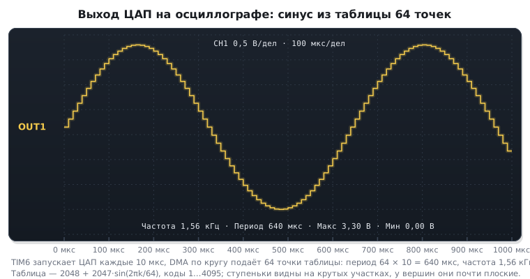
With a trigger every 10 µs and a table of 64 points you get a sine
of about 1.56 kHz. To change the frequency, change the timer's ARR;
the table does not need to be touched.
On an oscilloscope this is a stepped sine — 64 steps per period:
How many points to take. A trade-off: more points give a smoother signal, but a lower
maximum frequency and more memory. For sound 256 points are usually taken,
for auxiliary signals 32–64 are enough. The table is computed in advance and placed
in const so that it stays in Flash.
15.5 Built-in generators
Besides the table, the block has two modes of its own: triangle
and pseudo-random noise. The amplitude is set, the shape is computed in hardware,
no table or DMA is needed at all. The generator takes a step only on a trigger
(TEN1 = 1, the source is TSEL1, usually a timer): without a trigger there is no
triangle. A triangle with amplitude MAMP1 = 2ⁿ − 1 rises and falls
by one, so the period is about 2 · 2ⁿ triggers: with a trigger every 10 µs
and amplitude 4095 that is 8190 triggers, 12 Hz. The value of DHR12R1 is added
as an offset.
The triangle is handy for sweeps and checking the linearity of a circuit, the noise for testing filters and adding dither.
15.6 🔧 An electronic load: the DAC sets the current
An instrument for testing power supplies and batteries: it draws exactly the set current, whatever the voltage. It is built from a DAC, an op-amp, a MOSFET and a shunt:
ЦАП (PA4)       → вход «+» ОУ
выход ОУ        → затвор MOSFET
исток MOSFET    → шунт 1 Ом → земля
верх шунта      → вход «−» ОУ
сток MOSFET     → проверяемый источник
The amplifier (section 56) adjusts the gate so that the voltage on the shunt
equals the DAC voltage. So the current through the transistor and the shunt equals
U_ЦАП / R, and it does not depend on the source voltage. The MOSFET (section 52)
works here not as a switch but as a regulating element — in the linear region.
The DAC buffer is switched off. The amplifier input is high-impedance and does not load the output, and without the buffer the scale reaches zero (15.3) — the load can be set to zero current as well.
#define VREF_MV    3300u
#define R_SHUNT_MO 1000u                    /* шунт 1 Ом, в миллиомах */
#define I_MAX_MA   1000u                    /* программный предел нагрузки */

/* код ЦАП для тока в миллиамперах: U = I·R, код = U·4095 / Vref, с округлением */
uint32_t load_code(uint32_t ma)
{
    if (ma > I_MAX_MA)
        ma = I_MAX_MA;
    return (uint32_t)(((uint64_t)ma * R_SHUNT_MO * 4095u + VREF_MV * 500u) / (VREF_MV * 1000u));
}

void load_dac_init(void)
{
    RCC->AHB1ENR |= RCC_AHB1ENR_GPIOAEN;
    RCC->APB1ENR |= RCC_APB1ENR_DACEN;
    GPIOA->MODER |= GPIO_MODER_MODER4;      /* PA4 — аналоговый */
    DAC->DHR12R1 = 0;                       /* старт с нулевого тока */
    DAC->CR = DAC_CR_BOFF1 | DAC_CR_EN1;    /* буфер выключен: вход ОУ высокоомный, шкала до нуля */
}

void load_set_ma(uint32_t ma)
{
    DAC->DHR12R1 = load_code(ma);
}
What the scale gives. With a 3.3 V reference and a 1 Ω shunt one code is 0.806 mA. The software limit of 1 A is code 1241; anything higher is clamped. The integer conversion with rounding is off by no more than half a step — 0.403 mA over the whole 0–1000 mA scale.
The op-amp offset eats the bottom of the scale. On a 1 Ω shunt every millivolt of offset is a milliampere of error, and the DAC step is only 0.806 mA. The offset of an ordinary amplifier is about 3 mV (section 56): in the model with +3 mV the load at code 0 draws 3.05 mA, and with −3 mV codes 0–3 give no current at all, and it appears only from the fourth. So the op-amp is chosen with an input range down to ground and low offset, and the zero is calibrated.
The loop may ring. The gate is a capacitive load for the op-amp (section 163), and the feedback here is taken not from the amplifier output but from the shunt, after the transistor. The isolation resistor from 163.3 on its own does harm here: in a model with a 1 MHz amplifier a 10 % current step gives an overshoot of 1 to 24 % without the resistor and 8 to 45 % with a 470 Ω resistor in the gate. What works is a pair: a 220 Ω resistor in the gate and local feedback — the shunt is connected to the "−" input not by a wire but through 10 kΩ, and a 1 nF capacitor is placed from the op-amp output to the same input. There is no overshoot at 20 mA, at 0.5 A, or with a transistor of three times the capacitance; the price is settling of 7–8 µs at 0.5 A and about 70 µs at 20 mA.
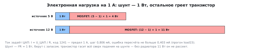
Where the power goes. At 1 A the shunt dissipates 1 W (I²R), so the resistor needs a margin. But the main heating is in the transistor: it drops everything the source supplies above the drop on the shunt. At 12 V and 1 A this is (12 − 1) × 1 = 11 W, at 5 V 4 W. Without a heatsink the transistor cannot dissipate such power.
The transistor is chosen by its safe operating area. It works right at the threshold: in the model of section 171 a current of 1 A at 11 V on the drain means 1.87 V on the gate, and a patch of the die 60 °C hotter would, with the same gate voltage, pass 2.5 A (171.5). The hot spot takes the current and heats further — the die burns out in a spot sooner than the thermal resistance promises. So you look at the safe operating area (SOA) graph — the constant-current (DC) line at the required voltage — not the on-resistance. If the graph has no DC line, the transistor is not rated for such operation.
15.7 Pitfalls
Your chip has no DAC. Check the datasheet before laying out the board.
The pin is not in analog mode. The digital buffer stays connected and interferes.
It does not reach the ends of the scale. The output buffer is on — this is its normal behaviour, not a fault.
The output "sags" under load. The buffer is off and the load is low-impedance. The DAC is not a power supply: a real load needs an amplifier.
The signal is stepped. Too few points in the table or no filter at the output. The DAC outputs steps by design; smoothing is the job of an external RC network.
The signal frequency is not what was calculated. You forgot that a timer on APB1 gets twice the bus frequency (section 13).
Noise on the supply. The analog output is as sensitive to supply quality as the ADC input: the same requirements for grounding and decoupling.
The electronic load does not go down to zero. The DAC output buffer is on:
the lowest codes do not reach zero (15.3). The amplifier input does not need the buffer —
the BOFF1 bit (15.6).
15.8 Summary
- A DAC is far from universal: the BluePill and the F401/F411 do not have one. Check the datasheet of the specific chip.
- Without a DAC, slow signals are made with PWM and an RC filter.
- Voltage =
код × Vref / 4095; the three data registers differ only in alignment. - The output buffer drives a load from 5 kΩ — fractions of a milliampere — at the cost of losing the ends of the scale; without it the output resistance is up to 15 kΩ.
- An arbitrary waveform generator is built as "table → DMA → DAC" triggered by a timer; frequency = trigger rate / number of points.
- Declare the table
const— it stays in Flash. - The built-in triangle and noise modes work without any table at all.
- An electronic load is a DAC, an op-amp, a MOSFET and a shunt: the current equals
U_ЦАП / R, the DAC buffer is off, and the power(U_ист − I·R) · Iheats the transistor. - The op-amp for the load needs low offset (3 mV on a 1 Ω shunt is almost four DAC steps) and local feedback against ringing; the transistor is chosen by the DC line of the safe operating area.
Next: section 15а "The new-style ADC on the G4" — differential input, oversampling to 16 bits and two calibrations.