 Embedded HandbookApps
14а. ADC errors: offset, gain, nonlinearity and noise — what can be calibrated and what cannot
Section 14 taught how to get a code and convert it to millivolts, section 15а how to switch on the G4 ADC with two calibrations, section 180 how not to spoil the signal before the input. Here — how far that code can be trusted: what the error is made of, what the datasheet promises, what the built-in calibration removes, what you have to remove yourself and what nothing removes.
Prerequisites: datasheets STM32F103x8/B (DS5319, also known as DocID13587, rev. 17), STM32F405/407 (DS8626, rev. 9) and STM32G474 (DS12288, rev. 5); reference manuals RM0008, RM0090 and RM0440; the CMSIS headers of the three series and LL for the F4 and G4. The numbers of the experiments come from an ADC model on a computer: a C program and an independent recomputation in Python gave the same lines. The calibration functions were built for Cortex-M3 and Cortex-M4. Not checked on hardware.
Terms used in the documentation
Term Meaning offset error (EO) shift of the whole transfer characteristic gain error (EG) error at the top of the scale differential linearity error (ED, DNL) deviation of a step width from its ideal integral linearity error (EL, INL) deviation of transitions from a straight line total unadjusted error (ET, TUE) the full error with no corrections end point correlation line the straight line through the end transitions effective number of bits (ENOB) resolution actually achieved, with noise signal-to-noise and distortion ratio (SINAD) signal power against noise plus distortion code density test finding transitions from a histogram of codes calibration factor (CALFACT) the stored correction value input leakage current (Ilkg) current flowing into or out of the pin dither adding a small signal so codes change
14а.1 What the error is made of
An ideal 12-bit ADC changes the code every time the input passes the next fraction of the reference: 1 LSB = VREF+ / 4096 — at 3.3 V this is 805.7 µV. A real one changes the code at other points. The datasheet measures all errors in LSB and defines them through the transition thresholds (DS8626, figure 49; DS12288, figure 28; figure 37 of DS5319 has the same words, but the line about EO contains a typo — "between the first and the last actual transition"):
- EO, offset error — how far the first actual transition is from the first ideal one. The whole characteristic is shifted.
- EG, gain error — how far the last actual transition is from the last ideal one. In this definition EG also includes the offset; the pure slope error is the difference EG − EO.
- ED, differential nonlinearity — the largest deviation of a step width from 1 LSB. ED = −1 means the code is missing altogether.
- EL, integral nonlinearity — the largest deviation of a transition from the straight line drawn through the end transitions. Offset and slope have already been subtracted from it.
- ET, total unadjusted error — the largest deviation of the actual characteristic from the ideal one. This is what a program that calibrates nothing gets.
ET is not the sum of the others: the errors reach their maxima at different points of the scale and may have different signs. On the F103 over the full supply range the largest EO + EG + EL give 8.5 LSB, the root of the sum of squares 4.9, and the table gives ET as 5.
Four more sources are added to these five, and they are not in the "ET" line:
- Noise. With a constant input the code "jitters". It is measured in LSB rms, and on a sine wave by the SINAD ratio, from which the effective number of bits is computed: ENOB = (SINAD − 1.76) / 6.02.
- The reference. The code is a fraction of VREF+ (14.9). If the reference is 1 % off, all readings are 1 % off: from outside this is indistinguishable from a gain error.
- Source resistance. The sampling capacitor did not have time to charge (14.2, 180.1). The F103 datasheet formula: RAIN < TS / (fADC · CADC · ln 2^(N+2)) − RADC, the condition being an error under a quarter of an LSB. With N = 12 that is ln 2^14 = 9.70 time constants; with CADC = 8 pF, RADC = 1 kΩ and 14 MHz the formula reproduces the table from 14.2: 0.4 kΩ at 1.5 cycles, 5.9 kΩ at 7.5 and 50.1 kΩ at 55.5 (the table says 50).
- Input leakage. The pin leakage current flows through the source resistance. The F103 and F407 datasheets promise no more than ±1 µA; on a 10 kΩ source that is 10 mV — 12.4 LSB, on 50 kΩ it is 50 mV, 62.1 LSB. This is a datasheet limit, not a property of the individual chip: there is nothing to calibrate it with, leakage is avoided with a buffer or a lower-impedance source (180.2).
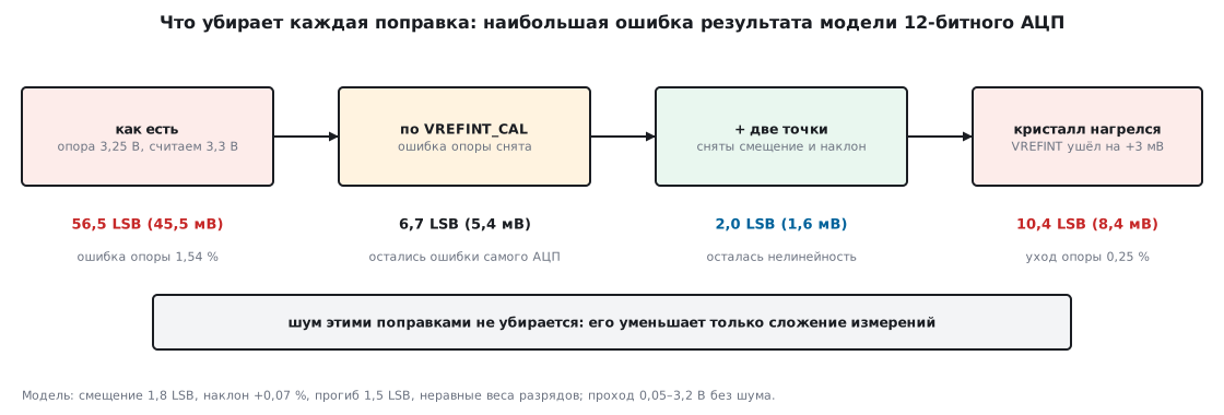
What removes what — on the model from 14а.4:
14а.2 What the datasheets promise
Typical and maximum values, in LSB:
| F103, table 48 | F103, table 49 | F407, table 68 | G474, table 68 | |
|---|---|---|---|---|
| conditions | 25 °C, 3–3.6 V | 2.4–3.6 V | 1.8–3.6 V | 25 °C, 3 V |
| ET | ±1.3 / ±2 | ±2 / ±5 | ±2 / ±5 | 5.9 / 6.9 |
| EO | ±1 / ±1.5 | ±1.5 / ±2.5 | ±1.5 / ±2.5 | 2.5 / 4 |
| EG | ±0.5 / ±1.5 | ±1.5 / ±3 | ±1.5 / ±3 | 4.6 / 6.6 |
| ED | ±0.7 / ±1 | ±1 / ±2 | ±1 / ±2 | 1.1 / 1.9 |
| EL | ±0.8 / ±1.5 | ±1.5 / ±3 | ±1.5 / ±3 | 2.3 / 3.4 |
How to read these numbers:
- On the F103 the ADC clock is 14 MHz, on the F407 30 MHz, the source no more than 10 kΩ. On the G474 — a single-ended input, a fast channel at 4 million conversions per second, without oversampling; for a differential input the numbers are smaller (ET 4.6 / 5.6).
- For the F103 and G474 the numbers are given after the built-in calibration — this is stated in the footnotes to the tables. Without it they do not apply.
- "Typical" is not the average: it is the limit within which 95 % of the dies of a batch fall. "Maximum" was obtained on a sample of dies or by calculation — so the footnotes say — and is not tested in production.
- Room temperature and a narrow supply range give ET ±2 on the F103, the full range ±5. The datasheet says it plainly: under narrower conditions the accuracy is better.
- 5 LSB out of 4096 is 0.12 % of the scale, 4.0 mV at 3.3 V.
For the G474 the datasheet also gives dynamic figures — on a sine wave, for the same fast channel: SINAD at least 64.4 dB, typically 65.6 dB; ENOB at least 10.4, typically 10.6 bits. The formula from 14а.1 gives 10.41 and 10.60 from these SINAD values — that is, the ENOB in the table is simply recomputed from SINAD. Almost one and a half bits out of twelve are eaten by noise and distortion.
Separately — the internal reference VREFINT, from which the supply is computed:
| F103 | F407 | G474 | |
|---|---|---|---|
| VREFINT: min / typical / max, V | 1.16 / 1.20 / 1.26 | 1.18 / 1.21 / 1.24 | 1.182 / 1.212 / 1.232 |
| spread from typical | −3.3 % / +5.0 % | −2.5 % / +2.5 % | −2.5 % / +1.7 % |
| drift over temperature, typical / maximum | — / 10 mV | 3 / 5 mV | 5 / 7.5 mV |
| the same drift at full scale | 34 LSB | 10 / 17 LSB | 17 / 25 LSB |
| temperature coefficient, ppm/°C | up to 100 | 30 / 50 | 30 / 50 |
| factory code | none | 30 °C, 3.3 V | 30 °C, 3.0 V |
The spread between dies is removed by the factory code (14а.5). Nothing removes the drift over temperature: 5 mV out of 1.21 V is 0.41 %, 17 LSB at full scale. That is more than all the errors of the ADC itself. For the G474 the datasheet also names ageing: typically 300 ppm per 1000 hours, up to 1000 ppm.
14а.3 What the built-in calibration corrects
F1: the CAL and RSTCAL bits in ADC_CR2. RM0008 (11.4): calibration reduces
the errors due to the spread of the internal capacitors — a correction code is computed
for each capacitor, and in subsequent conversions its contribution is subtracted.
Before calibration the ADC must have been on for at least two cycles; it lasts
83 cycles — 5.9 µs at 14 MHz. When it ends the calibration codes appear in
ADC_DR. Both RM0008 and the datasheet advise calibrating after every power-on.
G4: the ADCAL bit in ADC_CR. RM0440 (21.4.8): calibration removes the offset
error, which varies from die to die. The factor is 7 bits, separate for
single-ended and differential inputs (ADCALDIF), both are kept in
ADC_CALFACT. It lasts 116 cycles — 1.93 µs at 60 MHz. The factor is lost
when power is removed from the ADC (Standby, VBAT) and in the ADC's deep power-down; it can be
saved and written back when the ADC is enabled and not converting. The RM advises
recalibrating if VREF+ has changed by more than 10 %.
F4: no calibration. In the ADC chapter of RM0090 the word calibration does not appear, the
stm32f407xx.h header has no ADC_CR2_CAL bit, the DS8626 accuracy table has
no "after calibration" footnote. There is nothing to start. There is something else — the factory
codes of VREFINT and the temperature sensor in system memory.
/* F103. АЦП уже включён первой записью ADON и выждал tSTAB (раздел 14.3). */
uint16_t adc_f1_calibrate(void)
{
    ADC1->CR2 |= ADC_CR2_RSTCAL;                /* сбросить калибровочные регистры */
    while (ADC1->CR2 & ADC_CR2_RSTCAL) {
    }
    ADC1->CR2 |= ADC_CR2_CAL;                   /* поправки на разброс конденсаторов */
    while (ADC1->CR2 & ADC_CR2_CAL) {
    }
    return (uint16_t)ADC1->DR;                  /* RM0008: коды калибровки попадают в ADC_DR */
}
/* G474. АЦП выключен (ADEN = 0), регулятор включён и выждал 20 мкс (раздел 15а.3).
   Возвращает ADC_CALFACT: его сохраняют перед Standby. */
uint32_t adc_g4_calibrate(void)
{
    ADC1->CR &= ~ADC_CR_ADCALDIF;               /* несимметричные входы: CALFACT_S */
    ADC1->CR |= ADC_CR_ADCAL;
    while (ADC1->CR & ADC_CR_ADCAL) {
    }
    ADC1->CR |= ADC_CR_ADCALDIF;                /* дифференциальные входы: CALFACT_D */
    ADC1->CR |= ADC_CR_ADCAL;
    while (ADC1->CR & ADC_CR_ADCAL) {
    }
    ADC1->CR &= ~ADC_CR_ADCALDIF;
    return ADC1->CALFACT;
}

/* Вернуть сохранённые коэффициенты: АЦП включён, измерений нет (RM0440, 21.4.8). */
int adc_g4_calfact_restore(uint32_t calfact)
{
    if (!(ADC1->CR & ADC_CR_ADEN) || (ADC1->CR & (ADC_CR_ADSTART | ADC_CR_JADSTART))) {
        return -1;
    }
    ADC1->CALFACT = calfact & (ADC_CALFACT_CALFACT_S | ADC_CALFACT_CALFACT_D);
    return 0;
}
/* F407. Калибровки в АЦП нет — есть заводские коды в системной памяти (DS8626, таблицы 70 и 73). */
#define F4_VREFINT_CAL  (*(const uint16_t *)0x1FFF7A2Au)    /* 30 °C, VDDA = 3,3 В */
#define F4_TS_CAL1      (*(const uint16_t *)0x1FFF7A2Cu)    /* 30 °C */
#define F4_TS_CAL2      (*(const uint16_t *)0x1FFF7A2Eu)    /* 110 °C */

int adc_f4_factory(uint16_t *vrefint_cal, uint16_t *ts_cal1, uint16_t *ts_cal2)
{
    *vrefint_cal = F4_VREFINT_CAL;
    *ts_cal1 = F4_TS_CAL1;
    *ts_cal2 = F4_TS_CAL2;
    /* незаписанная ячейка читается как 0xFFFF: заводских кодов нет */
    return (*vrefint_cal == 0xFFFFu || *ts_cal1 == 0xFFFFu || *ts_cal2 <= *ts_cal1) ? -1 : 0;
}
What the built-in calibration does not do. It knows nothing about the voltage outside: it has no external standard. So it does not touch the reference error at all. What remains after it in the ADC itself is visible in the tables of 14а.2: for the F103 and G474 offset, gain and nonlinearity are given there already after calibration. Noise, leakage and incomplete charging of the sampling capacitor it does not see either.
14а.4 An ADC model and how errors are measured
To see what each correction removes, you need an ADC with known errors. The model is an array of 4095 thresholds. It has an offset of 1.8 LSB, a slope error of +0.07 %, a smooth bow of 1.5 LSB in the middle of the scale and unequal weights of the five most significant bits (from −0.06 % to +0.12 %) — as in a real successive approximation ADC, where the weights are set by capacitors. The noise is 0.7 LSB.
static void adc_build(const adc_par_t *p, double *T)
{
    double w[12];
    for (int b = 0; b < 12; b++) {
        w[b] = (double)(1 << b) * (1.0 + p->e[b]);
    }
    T[0] = -1e30;
    for (int k = 1; k < NC; k++) {
        double W = 0.0, u = (double)k / 4096.0;
        for (int b = 0; b < 12; b++) {
            W += (double)((k >> b) & 1) * w[b];
        }
        T[k] = p->offs + (1.0 + p->gain) * (W + 4.0 * p->bow * u * (1.0 - u));
    }
}

static int adc_code(const double *T, double x)      /* сколько порогов не выше x */
{
    int lo = 0, hi = NC - 1;
    while (lo < hi) {
        int mid = (lo + hi + 1) / 2;
        if (T[mid] <= x) {
            lo = mid;
        } else {
            hi = mid - 1;
        }
    }
    return lo;
}
The code density test. The thresholds of a real ADC are not directly visible — only the codes are. The standard method: apply a slow ramp slightly wider than the scale and count how many times each code came up. A wide step collects more samples, a narrow one fewer; the cumulative sum gives the position of each threshold. Noise does not interfere here, it averages out.
static void histogram(double sigma)
{
    static uint32_t H[NC];
    uint32_t total = (uint32_t)HIST_LSB * HIST_PER_LSB, cum = 0;
    double dmax = 0.0;

    memset(H, 0, sizeof H);
    for (uint32_t i = 0; i < total; i++) {
        double x = -8.0 + ((double)i + 0.5) / (double)HIST_PER_LSB;
        H[adc_code(TR, x + sigma * gauss(101u, i))]++;
    }
    TE[0] = -1e30;
    for (int k = 1; k < NC; k++) {
        cum += H[k - 1];
        TE[k] = -8.0 + (double)cum / (double)HIST_PER_LSB;
        if (fabs(TE[k] - TR[k]) > dmax) {
            dmax = fabs(TE[k] - TR[k]);
        }
    }
A ramp of 1024 steps per LSB is 4 210 688 noisy conversions. The thresholds were found with an error of no more than 0.072 LSB:
| Error, LSB | From the model thresholds | From the histogram |
|---|---|---|
| EO | 1.802 | 1.815 |
| EG | 4.975 | 5.003 |
| pure slope, EG − EO | 3.173 | 3.188 |
| ED | −0.513 | −0.511 |
| EL, line through the end points | 1.918 | 1.932 |
| EL, best-fit line | −1.068 | −1.099 |
| ET | 5.830 | 5.878 |
EL depends on which straight line is considered ideal. STM32 datasheets take the line through the end transitions; the best-fit line (least squares) gives a number almost half as large — when comparing ADCs from different makers, check which method is named. The largest ED is at the transition from code 3071 to 3072: there the ten low bits are cleared and the next one is switched on.
Noise with a constant input. The input stays put, 65 536 conversions of an ideal ADC with 0.7 LSB noise: 6 different codes came up, the standard deviation is 0.755 LSB (rounding added to the noise). In bits this is 12 − log2(0.755 · √12) = 10.61. A sine on the same ADC gave SINAD 65.48 dB and ENOB 10.58 — the two methods agreed. And this is the same order as the typical 10.6 bits in the G474 datasheet: they correspond to a standard deviation of 0.762 LSB.
14а.5 What the program calibrates
Everything in integers. The code is in Q4 format: the sum of 16 conversions or one code multiplied by 16; full scale is 65 536.
The reference from VREFINT_CAL. RM0440 (21.4.33): VREF+ = VREF+ during the factory
measurement × VREFINT_CAL / VREFINT code. The factory measurement for the F407 is
30 °C and VDDA = 3.3 V, the code at address 0x1FFF 7A2A (DS8626, table 73); for the
G474 30 °C and VDDA = VREF+ = 3.0 V, address 0x1FFF 75AA (DS12288,
table 6). The F103 has no factory code. The same ratio brings any code
to the factory reference — then it can be compared with the factory points of the temperature
sensor and with your own calibration:
/* Микровольты по номиналу: середина кода, опора vref_uv. */
uint32_t adc_code_to_uv(uint32_t code_q4, uint32_t vref_uv)
{
    return (uint32_t)(((uint64_t)(code_q4 + 8u) * vref_uv) >> 16);
}

/* Опора VREF+ в микровольтах по коду VREFINT и заводскому коду, снятому при cal_vref_mv. */
uint32_t adc_vref_uv(uint32_t vrefint_q4, uint16_t vrefint_cal, uint32_t cal_vref_mv)
{
    uint64_t num = (uint64_t)cal_vref_mv * 1000u * ((uint32_t)vrefint_cal * 16u);
    return (uint32_t)((num + vrefint_q4 / 2u) / vrefint_q4);
}

/* Код, каким он был бы при заводской опоре: умножить на VREFINT_CAL / код VREFINT. */
uint32_t adc_norm_q4(uint32_t code_q4, uint32_t vrefint_q4, uint16_t vrefint_cal)
{
    return (code_q4 * ((uint32_t)vrefint_cal * 16u) + vrefint_q4 / 2u) / vrefint_q4;
}
The factory point itself is not exact: the reference during the measurement is held to ±10 mV, the temperature to ±5 °C (for the G474 this is written in the datasheet, for the F4 in the comments of the LL header). 10 mV out of 3.0 V is 0.33 %, 13.7 LSB at full scale; out of 3.3 V 0.30 %, 12.4 LSB.
Two points. Two known voltages are applied to the input — from an external source measured with a voltmeter — and the two codes are remembered. A straight line through two points removes both offset and slope. One point removes only the offset:
typedef struct {
    int32_t uv_lo;      /* напряжение нижней точки, мкВ */
    int32_t c_lo_q4;    /* код в нижней точке, Q4 */
    int32_t k_q16;      /* наклон: микровольт на единицу кода Q4, умноженный на 65536 */
} adc_cal2_t;
/* Одна точка: убрать только смещение, наклон — номинальный (vref_uv на 65536 единиц Q4). */
void adc_cal1_make(adc_cal2_t *cal, uint32_t c_q4, uint32_t uv, uint32_t vref_uv)
{
    cal->uv_lo = (int32_t)uv;
    cal->c_lo_q4 = (int32_t)c_q4;
    cal->k_q16 = (int32_t)vref_uv;
}

/* Две точки: коды c_lo_q4 и c_hi_q4 сняты при известных напряжениях uv_lo и uv_hi. */
int adc_cal2_make(adc_cal2_t *cal, uint32_t c_lo_q4, uint32_t uv_lo, uint32_t c_hi_q4, uint32_t uv_hi)
{
    if (c_hi_q4 <= c_lo_q4 || uv_hi <= uv_lo) {
        return -1;
    }
    cal->uv_lo = (int32_t)uv_lo;
    cal->c_lo_q4 = (int32_t)c_lo_q4;
    cal->k_q16 = (int32_t)((((uint64_t)(uv_hi - uv_lo)) << 16) / (c_hi_q4 - c_lo_q4));
    return 0;
}

/* Микровольты по калибровке. Сдвиг знакового числа у gcc и armclang арифметический. */
int32_t adc_cal2_apply(const adc_cal2_t *cal, uint32_t code_q4)
{
    int64_t p = (int64_t)((int32_t)code_q4 - cal->c_lo_q4) * cal->k_q16 + 32768;
    return cal->uv_lo + (int32_t)(p >> 16);
}
What came out. The model is calibrated at a reference of 3.300 V at the points 0.3 and 3.0 V (16 noisy conversions each), then the input is swept from 0.05 to 3.2 V without noise and the error of the result is examined. Signs are omitted:
| What was done | Reference during measurement | Largest error, LSB | mV | RMS, LSB |
|---|---|---|---|---|
| nothing, reference assumed to be 3.3 V | 3.25 V | 56.48 | 45.5 | 31.28 |
| nothing, reference assumed to be 3.3 V | 3.30 V | 6.33 | 5.1 | 4.54 |
| one point: offset | 3.30 V | 3.96 | 3.2 | 2.32 |
| two points | 3.30 V | 1.91 | 1.5 | 0.82 |
| two points and a nonlinearity table | 3.30 V | 1.07 | 0.9 | 0.37 |
| two points, then the supply dropped | 3.25 V | 62.08 | 50.0 | 35.10 |
reference from VREFINT_CAL |
3.25 V | 6.70 | 5.4 | 4.87 |
reference from VREFINT_CAL and two points |
3.25 V | 1.98 | 1.6 | 0.85 |
the same, VREFINT drifted by +3 mV |
3.25 V | 10.38 | 8.4 | 6.56 |
the same, VREFINT drifted by +5 mV |
3.25 V | 16.52 | 13.3 | 10.13 |
The table reads like this:
- A reference of 3.25 V instead of 3.3 is an error of 1.54 %, and on its own it is larger than all the others together: 56 LSB against 6.
- Two-point calibration also remembers the reference as it was that day. The supply dropped — the error came back in full (62 LSB). Calibration without recomputing the reference is suitable only where VREF+ is a separate precision source.
- Recomputing from
VREFINT_CALremoves the reference error (the model computed 3 249 432 µV against the true 3 250 000), but not the ADC errors: 6.7 LSB. - Together — 2.0 LSB: the nonlinearity remains. Two-point calibration does not touch it.
- All of this rests on
VREFINT. If it drifts by the 3 mV typical for the F407 — again 10.4 LSB, by the maximum 5 mV — 16.5. The result cannot be more accurate than the reference.
The temperature sensor. The factory points are 30 and 110 °C: for the F407 at 3.3 V
(0x1FFF 7A2C and 0x1FFF 7A2E), for the G474 at 3.0 V (0x1FFF 75A8 and
0x1FFF 75CA). The sensor code is first brought to the factory reference, otherwise a supply
error turns into a temperature error:
/* Температура в десятых долях градуса по двум заводским точкам. ts_q4 — код датчика,
   уже приведённый к заводской опоре (adc_norm_q4). */
int32_t adc_ts_x10(uint32_t ts_q4, uint16_t cal1, uint16_t cal2, int32_t t1_x10, int32_t t2_x10)
{
    int32_t den = ((int32_t)cal2 - (int32_t)cal1) * 16;
    int32_t num = ((int32_t)ts_q4 - (int32_t)cal1 * 16) * (t2_x10 - t1_x10);

    if (den <= 0) {
        return t1_x10;
    }
    return t1_x10 + (num + (num >= 0 ? den / 2 : -den / 2)) / den;
}
In the model the die is at 85 °C, the reference 3.25 V: with the conversion the result is 85.0 °C, without it 90.6 °C.
A nonlinearity table. The bow can be subtracted with a table: 17 nodes every 256 codes, linear between the nodes.
/* Поправка нелинейности: 17 узлов через 256 кодов, значения в единицах Q4, между узлами — по прямой. */
uint32_t adc_inl_apply(const int8_t lut[17], uint32_t code_q4)
{
    uint32_t seg = code_q4 >> 12;
    int32_t frac = (int32_t)(code_q4 & 0xFFFu);
    int32_t corr;

    if (seg > 15u) {
        return code_q4;
    }
    corr = (lut[seg] * (4096 - frac) + lut[seg + 1u] * frac + 2048) >> 12;
    return (uint32_t)((int32_t)code_q4 + corr);
}
In the model it reduced the largest error from 1.91 to 1.07 LSB. But the table had to be taken from this very chip with a histogram of four million conversions, from a source more linear than the ADC itself. The datasheet does not give the nonlinearity of a particular die — only the limits for a batch. The gain is under 1 LSB with noise of 0.7 LSB. If you need such linearity, it is cheaper to take an external ADC.
Size. All ten functions of the file are 294 bytes for both Cortex-M3 and
Cortex-M4 (arm-none-eabi-gcc -Os); adc_cal2_apply is 30 bytes, adc_norm_q4
14. Two functions need 64-bit division: the compiler calls
the library __aeabi_uldivmod and __aeabi_ldivmod. Both run rarely —
during calibration and when recomputing the reference, not on every conversion.
14а.6 Summing conversions: what it gives and what it does not
Section 15а.5 showed: with noise of 1 LSB every four summed conversions give about one bit. Here are the limits of this technique.
/* Сумма n измерений. 16 измерений 12-битного АЦП — код Q4. */
uint32_t adc_sum(uint16_t (*read)(void), unsigned n)
{
    uint32_t s = 0;
    while (n--) {
        s += read();
    }
    return s;
}

/* Передискретизация: 4^bits измерений дают результат на bits разрядов длиннее (bits = 0…4, до 16 бит). */
uint32_t adc_oversample(uint16_t (*read)(void), unsigned bits)
{
    uint32_t s = adc_sum(read, 1u << (2u * bits));
    return bits ? (s + (1u << (bits - 1u))) >> bits : s;
}
ENOB on a sine (4096 points, each the sum of N conversions):
| Summed N | Ideal ADC, noise 0.7 LSB | Ideal, noise 0.05 LSB | The same plus a 1 LSB ramp | Model with errors, noise 0.7 LSB |
|---|---|---|---|---|
| 1 | 10.58 | 11.93 | 11.93 | 10.28 |
| 4 | 11.58 | 12.15 | 13.70 | 10.75 |
| 16 | 12.60 | 12.20 | 14.77 | 10.93 |
| 64 | 13.61 | 12.23 | 15.77 | 10.99 |
| 256 | 14.63 | 12.23 | 16.78 | 11.00 |
- There is noise, and it is random — one bit for every four conversions, from 10.58 to 14.63.
- There is little noise — summing is useless: all N conversions give the same code. 256 conversions instead of one added 0.3 bits.
- Dither. A known signal is added to the quiet input which over N conversions covers exactly 1 LSB and averages to zero — a ramp from a DAC or PWM with an RC filter. The codes start to change, and summing works again: 16.78 bits with 256 conversions. Random noise does the same, but worse: with 0.7 LSB of noise the same 256 conversions gave 14.63 (on noise dither — section 165.8).
- Nonlinearity does not average out. For the model with errors ENOB hits a ceiling at 11.0: the distortion from the bow is the same in every conversion.
The same with a constant input — the rms error of the result in LSB, 257 voltages over the whole scale:
| Summed N | Ideal ADC | Model without corrections | Model, two points |
|---|---|---|---|
| 1 | 0.768 | 4.622 | 1.078 |
| 16 | 0.188 | 4.547 | 0.772 |
| 256 | 0.050 | 4.551 | 0.765 |
For the ideal ADC the error falls fourfold for every 16 conversions. For a real one without calibration it stays put — 4.5 LSB of offset and slope cannot be removed by summing. After two-point calibration 0.77 LSB of nonlinearity remains, and there is no point summing more than 16 conversions. Sixteen bits in a register are not sixteen bits of accuracy.
14а.7 Pitfalls
"The ADC is 12 bits, so the accuracy is 0.8 mV". 0.8 mV is the weight of a code. The total error per the datasheet is up to 5 LSB on the F103 and F407, up to 6.9 on the G474, and that is without the reference.
Calibration was run, but the readings are still off by a few percent.
The built-in calibration does not know the reference. An error in percent is VREF+: it is
computed from VREFINT (14.9) or a separate reference source is fitted.
Calibrated at two points on the test bench, in the field the readings drifted.
The calibration remembered the bench reference: in the model 1.91 LSB became 62.08
when the supply dropped from 3.3 to 3.25 V. Before calibration and before every
conversion the code is brought to the factory reference (adc_norm_q4).
The G4 formula uses 3300. The G474 factory code was taken at 3.0 V, the F407 one at 3.3 V. Mix them up and the error is 10 % (14.10).
The die temperature is off by several degrees with a flat battery. The sensor code was not brought to the factory reference: in the model 90.6 °C instead of 85.0 at 3.25 V.
256 conversions were summed and the result is considered 16-bit. Summing removes only random noise. Offset, slope and nonlinearity remain: in the model 4.5 LSB both before and after.
Summing gave nothing. The noise is below a fraction of an LSB — all conversions are the same. A dithered ramp or noise is needed.
The accuracy table does not apply. For the F103 and G474 it is given after the built-in
calibration. On the G4 the calibration is lost in Standby — repeat it or restore
the saved ADC_CALFACT.
A high-impedance source shifts the readings. Input leakage of up to 1 µA through 10 kΩ is 12.4 LSB. A buffer or a lower-impedance source (180.2).
Warm-up moves the readings although everything is calibrated. VREFINT drifts with
temperature by 3–7.5 mV — 10–25 LSB at full scale. If higher accuracy is needed —
an external voltage reference (section 177).
14а.8 Summary
- The datasheet measures ADC errors in LSB from the transition thresholds: offset EO, gain EG, nonlinearities ED and EL, total error ET. ET is not the sum of the others: on the F103 8.5 LSB as a sum, 5 in the table.
- Promised: ET up to ±5 LSB on the F103 and F407, up to 6.9 on the G474; G474 ENOB typically 10.6 bits at SINAD 65.6 dB, ENOB = (SINAD − 1.76) / 6.02.
- Built-in calibration: on the F1 (
CAL,RSTCAL) the capacitor spread, 83 cycles; on the G4 (ADCAL,ADC_CALFACT) the offset, 7 bits, 116 cycles; the F4 does not have it. It does not touch the reference, slope or nonlinearity. - The reference error is larger than all the others: 1.54 % — 56 LSB against 6 for the ADC itself.
It is removed by
VREFINT_CAL(F407: 3.3 V,0x1FFF 7A2A; G474: 3.0 V,0x1FFF 75AA), with the accuracy of the factory point — 0.3 %. - Two-point calibration with conversion to the factory reference: from 56.5 to 2.0 LSB. The nonlinearity remains; a 17-node table gives another 0.8 LSB and is rarely worth it.
- The drift of
VREFINTover temperature (3–7.5 mV, 10–25 LSB) cannot be calibrated. - Summing N conversions removes random noise — one bit for every 4 conversions — and nothing else. Without noise it is useless until a ramp is added.
- Ten integer conversion functions — 294 bytes on Cortex-M3.
Full sources
adc_cal.h — integer conversion and calibration of ADC results — declarations.
/* Пересчёт и калибровка результатов АЦП в целых числах — раздел 14а.
   Код в формате Q4: сумма 16 измерений (или один код, умноженный на 16); полная шкала 12 бит — 65536. */
#ifndef ADC_CAL_H
#define ADC_CAL_H

#include <stdint.h>

typedef struct {
    int32_t uv_lo;      /* напряжение нижней точки, мкВ */
    int32_t c_lo_q4;    /* код в нижней точке, Q4 */
    int32_t k_q16;      /* наклон: микровольт на единицу кода Q4, умноженный на 65536 */
} adc_cal2_t;

uint32_t adc_sum(uint16_t (*read)(void), unsigned n);
uint32_t adc_oversample(uint16_t (*read)(void), unsigned bits);
uint32_t adc_code_to_uv(uint32_t code_q4, uint32_t vref_uv);
uint32_t adc_vref_uv(uint32_t vrefint_q4, uint16_t vrefint_cal, uint32_t cal_vref_mv);
uint32_t adc_norm_q4(uint32_t code_q4, uint32_t vrefint_q4, uint16_t vrefint_cal);
void adc_cal1_make(adc_cal2_t *cal, uint32_t c_q4, uint32_t uv, uint32_t vref_uv);
int adc_cal2_make(adc_cal2_t *cal, uint32_t c_lo_q4, uint32_t uv_lo, uint32_t c_hi_q4, uint32_t uv_hi);
int32_t adc_cal2_apply(const adc_cal2_t *cal, uint32_t code_q4);
uint32_t adc_inl_apply(const int8_t lut[17], uint32_t code_q4);
int32_t adc_ts_x10(uint32_t ts_q4, uint16_t cal1, uint16_t cal2, int32_t t1_x10, int32_t t2_x10);

#endif
adc_cal.c — integer conversion and calibration of ADC results.
/* Пересчёт и калибровка результатов АЦП в целых числах — раздел 14а.
   Файл без регистров: собирается и для Cortex-M, и на компьютере (модель adc_model.c вызывает эти же функции). */
#include "adc_cal.h"

/* Сумма n измерений. 16 измерений 12-битного АЦП — код Q4. */
uint32_t adc_sum(uint16_t (*read)(void), unsigned n)
{
    uint32_t s = 0;
    while (n--) {
        s += read();
    }
    return s;
}

/* Передискретизация: 4^bits измерений дают результат на bits разрядов длиннее (bits = 0…4, до 16 бит). */
uint32_t adc_oversample(uint16_t (*read)(void), unsigned bits)
{
    uint32_t s = adc_sum(read, 1u << (2u * bits));
    return bits ? (s + (1u << (bits - 1u))) >> bits : s;
}

/* Микровольты по номиналу: середина кода, опора vref_uv. */
uint32_t adc_code_to_uv(uint32_t code_q4, uint32_t vref_uv)
{
    return (uint32_t)(((uint64_t)(code_q4 + 8u) * vref_uv) >> 16);
}

/* Опора VREF+ в микровольтах по коду VREFINT и заводскому коду, снятому при cal_vref_mv. */
uint32_t adc_vref_uv(uint32_t vrefint_q4, uint16_t vrefint_cal, uint32_t cal_vref_mv)
{
    uint64_t num = (uint64_t)cal_vref_mv * 1000u * ((uint32_t)vrefint_cal * 16u);
    return (uint32_t)((num + vrefint_q4 / 2u) / vrefint_q4);
}

/* Код, каким он был бы при заводской опоре: умножить на VREFINT_CAL / код VREFINT. */
uint32_t adc_norm_q4(uint32_t code_q4, uint32_t vrefint_q4, uint16_t vrefint_cal)
{
    return (code_q4 * ((uint32_t)vrefint_cal * 16u) + vrefint_q4 / 2u) / vrefint_q4;
}

/* Одна точка: убрать только смещение, наклон — номинальный (vref_uv на 65536 единиц Q4). */
void adc_cal1_make(adc_cal2_t *cal, uint32_t c_q4, uint32_t uv, uint32_t vref_uv)
{
    cal->uv_lo = (int32_t)uv;
    cal->c_lo_q4 = (int32_t)c_q4;
    cal->k_q16 = (int32_t)vref_uv;
}

/* Две точки: коды c_lo_q4 и c_hi_q4 сняты при известных напряжениях uv_lo и uv_hi. */
int adc_cal2_make(adc_cal2_t *cal, uint32_t c_lo_q4, uint32_t uv_lo, uint32_t c_hi_q4, uint32_t uv_hi)
{
    if (c_hi_q4 <= c_lo_q4 || uv_hi <= uv_lo) {
        return -1;
    }
    cal->uv_lo = (int32_t)uv_lo;
    cal->c_lo_q4 = (int32_t)c_lo_q4;
    cal->k_q16 = (int32_t)((((uint64_t)(uv_hi - uv_lo)) << 16) / (c_hi_q4 - c_lo_q4));
    return 0;
}

/* Микровольты по калибровке. Сдвиг знакового числа у gcc и armclang арифметический. */
int32_t adc_cal2_apply(const adc_cal2_t *cal, uint32_t code_q4)
{
    int64_t p = (int64_t)((int32_t)code_q4 - cal->c_lo_q4) * cal->k_q16 + 32768;
    return cal->uv_lo + (int32_t)(p >> 16);
}

/* Поправка нелинейности: 17 узлов через 256 кодов, значения в единицах Q4, между узлами — по прямой. */
uint32_t adc_inl_apply(const int8_t lut[17], uint32_t code_q4)
{
    uint32_t seg = code_q4 >> 12;
    int32_t frac = (int32_t)(code_q4 & 0xFFFu);
    int32_t corr;

    if (seg > 15u) {
        return code_q4;
    }
    corr = (lut[seg] * (4096 - frac) + lut[seg + 1u] * frac + 2048) >> 12;
    return (uint32_t)((int32_t)code_q4 + corr);
}

/* Температура в десятых долях градуса по двум заводским точкам. ts_q4 — код датчика,
   уже приведённый к заводской опоре (adc_norm_q4). */
int32_t adc_ts_x10(uint32_t ts_q4, uint16_t cal1, uint16_t cal2, int32_t t1_x10, int32_t t2_x10)
{
    int32_t den = ((int32_t)cal2 - (int32_t)cal1) * 16;
    int32_t num = ((int32_t)ts_q4 - (int32_t)cal1 * 16) * (t2_x10 - t1_x10);

    if (den <= 0) {
        return t1_x10;
    }
    return t1_x10 + (num + (num >= 0 ? den / 2 : -den / 2)) / den;
}
adc_regs.c — built-in calibration and factory codes at register level on the F1, F4 and G4.
/* Встроенная калибровка и заводские коды по регистрам — раздел 14а.
   Заголовок серии подключает сборка: -include stm32f10x.h, stm32f4xx.h или stm32g4xx.h. */
#include <stdint.h>

#if defined(STM32F10X_MD)

/* F103. АЦП уже включён первой записью ADON и выждал tSTAB (раздел 14.3). */
uint16_t adc_f1_calibrate(void)
{
    ADC1->CR2 |= ADC_CR2_RSTCAL;                /* сбросить калибровочные регистры */
    while (ADC1->CR2 & ADC_CR2_RSTCAL) {
    }
    ADC1->CR2 |= ADC_CR2_CAL;                   /* поправки на разброс конденсаторов */
    while (ADC1->CR2 & ADC_CR2_CAL) {
    }
    return (uint16_t)ADC1->DR;                  /* RM0008: коды калибровки попадают в ADC_DR */
}

#elif defined(STM32F407xx)

/* F407. Калибровки в АЦП нет — есть заводские коды в системной памяти (DS8626, таблицы 70 и 73). */
#define F4_VREFINT_CAL  (*(const uint16_t *)0x1FFF7A2Au)    /* 30 °C, VDDA = 3,3 В */
#define F4_TS_CAL1      (*(const uint16_t *)0x1FFF7A2Cu)    /* 30 °C */
#define F4_TS_CAL2      (*(const uint16_t *)0x1FFF7A2Eu)    /* 110 °C */

int adc_f4_factory(uint16_t *vrefint_cal, uint16_t *ts_cal1, uint16_t *ts_cal2)
{
    *vrefint_cal = F4_VREFINT_CAL;
    *ts_cal1 = F4_TS_CAL1;
    *ts_cal2 = F4_TS_CAL2;
    /* незаписанная ячейка читается как 0xFFFF: заводских кодов нет */
    return (*vrefint_cal == 0xFFFFu || *ts_cal1 == 0xFFFFu || *ts_cal2 <= *ts_cal1) ? -1 : 0;
}

void adc_f4_internal_on(void)
{
    ADC->CCR |= ADC_CCR_TSVREFE;                /* датчик температуры и VREFINT: каналы 16 и 17 */
}

#elif defined(STM32G474xx)

/* G474. АЦП выключен (ADEN = 0), регулятор включён и выждал 20 мкс (раздел 15а.3).
   Возвращает ADC_CALFACT: его сохраняют перед Standby. */
uint32_t adc_g4_calibrate(void)
{
    ADC1->CR &= ~ADC_CR_ADCALDIF;               /* несимметричные входы: CALFACT_S */
    ADC1->CR |= ADC_CR_ADCAL;
    while (ADC1->CR & ADC_CR_ADCAL) {
    }
    ADC1->CR |= ADC_CR_ADCALDIF;                /* дифференциальные входы: CALFACT_D */
    ADC1->CR |= ADC_CR_ADCAL;
    while (ADC1->CR & ADC_CR_ADCAL) {
    }
    ADC1->CR &= ~ADC_CR_ADCALDIF;
    return ADC1->CALFACT;
}

/* Вернуть сохранённые коэффициенты: АЦП включён, измерений нет (RM0440, 21.4.8). */
int adc_g4_calfact_restore(uint32_t calfact)
{
    if (!(ADC1->CR & ADC_CR_ADEN) || (ADC1->CR & (ADC_CR_ADSTART | ADC_CR_JADSTART))) {
        return -1;
    }
    ADC1->CALFACT = calfact & (ADC_CALFACT_CALFACT_S | ADC_CALFACT_CALFACT_D);
    return 0;
}

/* Заводские коды G474 сняты при 3,0 В (DS12288, таблицы 5 и 6). */
#define G4_VREFINT_CAL  (*(const uint16_t *)0x1FFF75AAu)    /* 30 °C, VDDA = VREF+ = 3,0 В */
#define G4_TS_CAL1      (*(const uint16_t *)0x1FFF75A8u)    /* 30 °C */
#define G4_TS_CAL2      (*(const uint16_t *)0x1FFF75CAu)    /* 110 °C */

int adc_g4_factory(uint16_t *vrefint_cal, uint16_t *ts_cal1, uint16_t *ts_cal2)
{
    *vrefint_cal = G4_VREFINT_CAL;
    *ts_cal1 = G4_TS_CAL1;
    *ts_cal2 = G4_TS_CAL2;
    return (*vrefint_cal == 0xFFFFu || *ts_cal1 == 0xFFFFu || *ts_cal2 <= *ts_cal1) ? -1 : 0;
}

#else
#error "серия не выбрана"
#endif
Next: section 15 "DAC" — the reverse task: getting a voltage from a number.