 Embedded HandbookApps
14. Analog-to-digital converter (ADC)
Everything that comes from the real world — temperature, current, the position of a wiper, battery voltage — comes in analog form. The ADC turns it into a number. The block seems simple, but this is exactly where plausible but wrong results are most often obtained.
Terms used in the documentation
Term Meaning successive approximation finding the code bit by bit, from the top sampling time the time the input charges the sampling capacitor conversion time the full time of one conversion regular / injected channel the main queue / the priority queue scan mode going through the whole channel sequence continuous mode restarting right after each conversion external trigger starting a conversion from a timer or pin analog watchdog threshold monitoring in hardware calibration measuring and removing the converter's own error reference voltage the voltage the full scale corresponds to source impedance the resistance of whatever drives the input factory calibration value a value measured and stored at the factory chip temperature sensor the sensor of the die's own temperature
14.1 How it works and what follows from it
Inside there is a capacitor that charges from the input, and a circuit that, step by step, finds the binary code. Two consequences follow, which determine everything else.
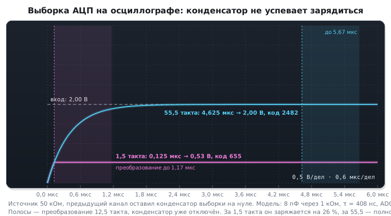
The capacitor needs time to charge. The higher the source resistance, the longer it takes. If you do not give it time, the result shifts towards the voltage that was on the capacitor, that is, towards the previous channel, and the error is stable and plausible.
The input is not free. The ADC loads the circuit being measured. A divider of megaohm resistors will be measured wrongly simply because it cannot recharge the capacitor in time.
Resolution and reference
The F1 and F4 have a resolution of 12 bits — 4096 steps. The code relates to the voltage as follows:
напряжение = код × Vref / 4095
With a 3.3 V reference one code is about 0.8 mV. The accuracy of the result cannot be better than the accuracy of the reference voltage: if the supply "floats" from 3.2 to 3.4 V, all measurements float with it.
14.2 Conversion time
время = (время выборки + время приближения) / ADCCLK
On the F1 the approximation time is 12.5 cycles, and the sampling time can be set from 1.5 to 239.5 cycles for each channel separately.
| Sampling | Total cycles | At 12 MHz |
|---|---|---|
| 1.5 | 14 | 1.17 µs |
| 13.5 | 26 | 2.17 µs |
| 55.5 | 68 | 5.67 µs |
| 239.5 | 252 | 21 µs |
How to choose. The minimum — 1.5 cycles — is enough only for a very low-impedance
source, such as an op-amp output. According to the F1 datasheet, at
ADCCLK = 14 MHz the source resistance must not exceed (at 12 MHz,
as in this section, the limits are slightly higher):
| Sampling, cycles | 1.5 | 7.5 | 13.5 | 28.5 | 41.5 | 55.5 |
|---|---|---|---|---|---|---|
| Source, at most | 0.4 kΩ | 5.9 kΩ | 11.4 kΩ | 25.2 kΩ | 37.2 kΩ | 50 kΩ |
Even a 10 kΩ / 10 kΩ divider (5 kΩ at the output) needs at least 7.5 cycles. For a high-impedance sensor or long wires take 55.5 or more; if the sampling must be short, put a capacitor to ground on the input — the charge is taken from it. The sign of too little time is readings that are low and depend on which channel was measured before.
What it looks like on the sampling capacitor if the source is a 50 kΩ sensor and the previous channel left zero on the capacitor:
⚠️ The ADC clock on the F1 must not exceed 14 MHz. With
PCLK2= 72 MHz the dividers 2, 4, 6, 8 are available — and only divider 6 or 8 stays within the limit. Set 2 or 4 and the block will keep working and producing numbers, but they will be wrong. No error occurs, no diagnostics at all:
c
RCC->CFGR &= ~RCC_CFGR_ADCPRE;
RCC->CFGR |= RCC_CFGR_ADCPRE_DIV6;   /* 12 MHz */
On the F4 the limit is higher — 36 MHz, and the dividers are different.
14.3 ⚠️ Calibration: mandatory on the F1
A key difference between the platforms.
| STM32F1 | STM32F4 | |
|---|---|---|
| calibration | performed by the program | there is no software calibration, nothing to start |
On the F1, after the block is switched on, calibration must be started — otherwise the error is noticeably above the datasheet figure:
ADC1->CR2 |= ADC_CR2_ADON;              /* первое включение: просыпается */
for (volatile int i = 0; i < 1000; i++) { }   /* пауза на стабилизацию */

ADC1->CR2 |= ADC_CR2_RSTCAL;            /* сброс калибровочного регистра */
while (ADC1->CR2 & ADC_CR2_RSTCAL) { }
ADC1->CR2 |= ADC_CR2_CAL;               /* сама калибровка */
while (ADC1->CR2 & ADC_CR2_CAL) { }
⚠️ The first write of
ADONonly switches the block on; it does not start a conversion. A pause is needed between switching on and calibration — the block needs time to stabilise. Starting a conversion is a second write ofADONto a block that is already on. The logic is not obvious, and people trip over it.
14.4 🔧 A single measurement
uint16_t adc1_read(uint8_t channel)
{
    ADC1->SQR3 = channel;               /* первым в очереди — нужный канал */
    ADC1->SQR1 = 0;                     /* длина очереди 1 */

    ADC1->CR2 |= ADC_CR2_ADON;          /* запуск */
    while (!(ADC1->SR & ADC_SR_EOC)) { }

    return (uint16_t)ADC1->DR;          /* чтение сбрасывает флаг */
}
Do not forget to put the pin into analog mode — on the F1 this is CNF = 00
with MODE = 00 (section 8). An input left digital gives readings
that look plausible but are distorted.
14.5 The channel sequence and modes
The ADC goes through not one input but a sequence — up to sixteen channels in any
order, with repeats. The order is set by the SQR registers.
| Mode | What it does |
|---|---|
| single | one conversion on command |
scan (SCAN) |
go through the whole sequence in one start |
continuous (CONT) |
start again right after finishing |
| external trigger | the conversion starts from a timer or a pin |
Regular and injected channels. Besides the main sequence there is a second, priority one: injected channels interrupt a normal conversion, do their own and hand control back. This is how something urgent is measured — for example, the current in a motor phase, synchronously with PWM — without breaking the background polling of sensors.
14.6 🔧 Scanning with DMA
Scanning without DMA is almost pointless: all channels share one result register, and the next conversion overwrites the previous one before the processor can read it. DMA picks up each result at once.
/* АЦП уже включён и откалиброван (14.3): последняя запись ADON — запуск.
   Время выборки каналов 0–3 при необходимости задают в SMPR2 (14.1). */
void adc1_scan_dma_init(void)
{
    RCC->AHBENR |= RCC_AHBENR_DMA1EN;

    /* ADC1 жёстко привязан к каналу 1 DMA1 — выбора нет. */
    DMA1_Channel1->CCR &= ~DMA_CCR1_EN;
    DMA1_Channel1->CPAR = (uint32_t)&ADC1->DR;
    DMA1_Channel1->CMAR = (uint32_t)adc_buf;
    DMA1_Channel1->CNDTR = 4;
    DMA1_Channel1->CCR = DMA_CCR1_MINC        /* адрес в памяти растёт */
                       | DMA_CCR1_CIRC        /* по кругу */
                       | DMA_CCR1_PSIZE_0     /* периферия: полуслово */
                       | DMA_CCR1_MSIZE_0     /* память: полуслово */
                       | DMA_CCR1_PL_1;
    DMA1_Channel1->CCR |= DMA_CCR1_EN;

    /* Очередь из четырёх каналов: 0, 1, 2, 3. */
    ADC1->SQR1 = (4u - 1u) << 20;             /* длина очереди */
    ADC1->SQR3 = (0u << 0) | (1u << 5) | (2u << 10) | (3u << 15);

    ADC1->CR1 |= ADC_CR1_SCAN;
    ADC1->CR2 |= ADC_CR2_DMA | ADC_CR2_CONT;
    ADC1->CR2 |= ADC_CR2_ADON;
}
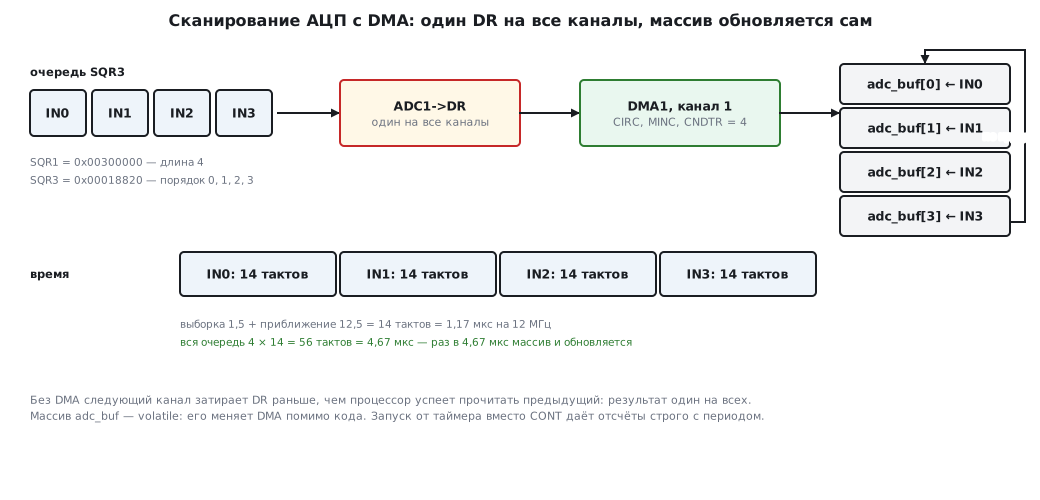
After that the values simply lie in the array and update themselves. The array must be
volatile — DMA changes it behind the code's back (section 3).
Triggering from a timer is the next step. Continuous mode digitises at maximum speed, which is rarely needed: you get a mountain of data with uneven intervals. It is more correct to start conversions from a timer, then the samples come strictly at the set period — and that is a mandatory condition for any subsequent signal processing.
The "timer → ADC → DMA" chain works with no involvement of the processor at all: it only takes apart the finished buffer.
14.7 Internal channels
Besides the external inputs there are two internal ones.
The die temperature sensor. It measures not the environment but the die itself, which heats up from operation. It is suitable for overheating control and rough estimates, but not for a weather station: the spread between individual chips is large.
The reference voltage VREFINT — about 1.2 V, stable regardless
of the supply. Hence a useful technique: measuring your own supply without a single
external part.
The logic is this: the VREFINT code gets smaller as the supply gets higher — after all, the reference
for the conversion is the supply. Knowing the exact value of VREFINT, VDDA is computed from its
code. On the F4 a factory calibration value lies in system memory,
which makes the estimate accurate.
The practical value: a battery-powered device can watch its discharge without spending pins, divider resistors or current on that divider.
14.8 Analog watchdog
The block compares the result with two thresholds and raises an interrupt when it goes out of bounds. The processor does not poll the values at all — it reacts only to the event.
The use is obvious: watching for overheating, a broken sensor, a supply dip. All without a single line in the main loop.
14.9 🔧 Millivolts without an external reference
The ADC code is a fraction of the reference voltage VREF+, not millivolts: code 0 is
zero volts, 4095 is VREF+ itself, whatever it happens to be right now. In packages
with up to 64 pins VREF+ is connected inside the die to the analog supply pin
VDDA; in larger packages it is a separate pin. On most boards it is
connected to the same supply, and then the reference is VDDA: while the supply is exactly
3.3 V, код × 3300 / 4095 is correct; let the battery drop to 3.0 V and all readings shift by 10 %.
If, however, a separate precision source (2.5 V, 2.048 V) sits on VREF+, the scale
does not depend on the supply, and the conversion below is not needed.
Finding the reference at every measurement is helped by the internal source VREFINT
(14.7): its voltage does not depend on the supply. There are two ways:
- from the nominal value in the datasheet —
VREF+ = номинал × 4095 / код_VREFINT; the accuracy is limited by the datasheet spread ofVREFINTitself: on the F103 it is from 1.16 to 1.24 V (up to +85 °C), and an estimate of 3.3 V varies from −106 to +114 mV from chip to chip. For accurate battery monitoringVREFINTis measured once at a known supply and the resulting calibration is kept in Flash memory; - from the factory code
VREFINT_CAL— it was taken at the factory atVREF+= 3.3 V, and it accounts for the spread of this particular die:VREF+ = 3300 × VREFINT_CAL / код_VREFINT.
The F4 has both; the F1 has no factory code — only the first. Further in the code
the reference is called vdda: on boards it is the supply.
F4: factory codes. System memory holds three numbers taken at the factory with a 3.3 V supply:
| Address | What | Conditions |
|---|---|---|
0x1FFF 7A2A |
VREFINT code |
3.3 V, 30 °C |
0x1FFF 7A2C |
temperature sensor code | 30 °C |
0x1FFF 7A2E |
temperature sensor code | 110 °C |
The addresses are from the LL driver for the whole F4 family (stm32f4xx_ll_adc.h),
the conditions from the same place: VREF+ = 3.3 V. Before use the cell should
be checked: unwritten Flash memory reads as 0xFFFF — that means there is no factory
value, and the nominal remains, as on the F1. From the factory code comes the reference,
and through it the millivolts of any channel and the temperature from two points.
All in integers:
/* питание VDDA по коду VREFINT: у F4 — по заводскому коду cal, снятому при 3,3 В */
uint32_t vdda_from_cal(uint16_t vref_code, uint16_t cal)
{
    return (3300u * cal + vref_code / 2u) / vref_code;
}

uint32_t code_to_mv(uint16_t code, uint32_t vdda_mv)
{
    return (code * vdda_mv + 2047u) / 4095u;
}

/* F4: температура кристалла по двум заводским точкам, в десятых долях градуса */
int32_t temp_x10(uint16_t ts_code, uint32_t vdda_mv, uint16_t cal30, uint16_t cal110)
{
    int32_t ts = (int32_t)((ts_code * vdda_mv + 1650u) / 3300u);   /* код, как при 3,3 В */
    return 300 + (ts - cal30) * 800 / (cal110 - cal30);
}
F1: no calibration. The nominal 1.2 V remains:
/* у F1 калибровки нет — только номинальные 1200 мВ */
uint32_t vdda_from_nominal(uint16_t vref_code)
{
    return (1200u * 4095u + vref_code / 2u) / vref_code;
}
An error of the reference becomes an error of the supply one to one: a reference 1 % below nominal — and 3.3 V will be computed as 3334 mV.
Enabling the internal channels. The TSVREFE bit on the F1 is in ADC1->CR2,
on the F4 in the common ADC->CCR. VREFINT is channel 17, the sensor on the F405/407 is channel 16.
The longest sampling time is used, because both sources are high-impedance:
239.5 cycles at 12 MHz — 20 µs, 480 cycles at 21 MHz — 23 µs.
void internal_channels_on(void)
{
    ADC->CCR    |= ADC_CCR_TSVREFE;                     /* включить датчик и VREFINT */
    ADC1->SMPR1 |= ADC_SMPR1_SMP16 | ADC_SMPR1_SMP17;   /* 111: 480 тактов — 23 мкс при 21 МГц */
}

uint32_t vdda_now(void)
{
    return vdda_from_cal(adc_read_ch(17), VREFINT_CAL_F4);
}

int32_t chip_temp_x10(void)                             /* канал 16 — датчик у F405/407 */
{
    uint32_t vdda = vdda_now();
    return temp_x10(adc_read_ch(16), vdda, TS_CAL30_F4, TS_CAL110_F4);
}
What the conversion showed. The functions were run on a computer against an ideal ADC:
supply from 2.0 to 3.6 V in 1 mV steps, temperature from −40 to 125 °C with a supply of
2.4–3.6 V. The factory codes were taken as an example: VREFINT 1.21 V (code 1502),
the sensor 0.76 V at 25 °C and 2.5 mV/°C (codes 959 and 1207).
| What was computed | Largest error |
|---|---|
VDDA from the VREFINT code |
2 mV |
| channel millivolts (1234 mV) | 1 mV |
| die temperature | 0.4 °C |
These are errors of rounding alone — from the resolution and integer arithmetic. The sensor itself is off by degrees and heats up together with the die (14.7).
14.10 F0 and G0: an ADC without a sequence
The F0 and G0 have one ADC, and it is built differently from the F1 and F4. The main difference is that there is no
SQR1…SQR3 sequence with channel positions: channels are simply marked with bits in
CHSELR, and the ADC goes through them in increasing number (SCANDIR — in the opposite
direction). The data is in DR at offset 0x40, the start is the ADSTART bit, end of
conversion is EOC, end of the whole mask is EOS. Calibration is mandatory in both
series and is done with the ADC disabled (ADEN = 0) — unlike the F1, where
the ADC is, on the contrary, switched on before calibration (14.3):
    ADC1->CR |= ADC_CR_ADCAL;                   /* калибровка — при выключенном АЦП */
    while (ADC1->CR & ADC_CR_ADCAL) {
    }
    ADC1->CR |= ADC_CR_ADEN;
    while (!(ADC1->ISR & ADC_ISR_ADRDY)) {
    }
One measurement — a channel mask instead of a number:
uint16_t adc_read_f0(uint32_t channel_mask)
{
    ADC1->CHSELR = channel_mask;                /* один бит на канал, не номер в SQR */
    ADC1->CR |= ADC_CR_ADSTART;
    while (!(ADC1->ISR & ADC_ISR_EOC)) {
    }
    return (uint16_t)ADC1->DR;
}
Code from the F1 does not build here — and that is good, the error is caught at once:
no member named 'SQR3' in 'ADC_TypeDef', the same for CR2.
What the G0 adds. Three things, each of which catches someone porting code from the F0:
- before calibration the ADC regulator is switched on —
ADVREGEN— and 20 µs are waited (the number is from LL:LL_ADC_DELAY_INTERNAL_REGUL_STAB_US); without this the ADC is silent; - after writing
CHSELRthe new mask does not take effect at once: wait for theCCRDYflag, otherwise the previous channel is measured; - the calibration factor is kept in its own register
CALFACT(0xB4) — it can be saved and restored after sleep.
    ADC1->CR |= ADC_CR_ADVREGEN;                /* сначала регулятор — и 20 мкс ожидания */
    wait_us(LL_ADC_DELAY_INTERNAL_REGUL_STAB_US);
    ADC1->ISR = ADC_ISR_CCRDY;                  /* флаг сбрасывается записью единицы */
    ADC1->CHSELR = channel_mask;
    while (!(ADC1->ISR & ADC_ISR_CCRDY)) {      /* у G0 смена каналов вступает не сразу */
    }
The G0 also has oversampling: the ADC itself adds up to 256 measurements and shifts the sum — a 16-bit result without the core:
ADC1->CFGR2 |= ADC_CFGR2_OVSE | LL_ADC_OVS_RATIO_256 | LL_ADC_OVS_SHIFT_RIGHT_4;
Clock and time. The ADC clock is synchronous from PCLK (CKMODE: /2, /4, on the G0
also /1) or its own asynchronous one; on the G0 the asynchronous one can be divided by PRESC up to 256.
Sampling time: on the F0 from 1.5 to 239.5 cycles, on the G0 from 1.5 to 160.5, and the G0
keeps two different times (SMP1, SMP2) and assigns one of them to each channel
with the SMPSEL bits. The listings use the longest time for VREFINT:
| F0 at 12 MHz | G0 at 16 MHz | |
|---|---|---|
| sampling + conversion, cycles | 239.5 + 12.5 = 252 | 160.5 + 12.5 = 173 |
| one measurement | 21 µs | 10.8 µs |
Internal channels and factory codes. The channel numbers differ between the series, and so do the conditions of the factory calibration:
| F0 | G0 | |
|---|---|---|
VREFINT channel |
17 | 13 |
| temperature sensor channel | 16 | 12 |
VREFINT code taken at VREF+ |
3.3 V | 3.0 V |
address of the VREFINT code |
0x1FFF F7BA |
0x1FFF 75AA |
| temperature sensor points | 30 and 110 °C | 30 and 130 °C |
Not every F0 has two sensor points: the F030 and F070 have a single factory point —
TS_CAL1 at 30 °C, and the datasheet slope is used.
So the formula from 14.9 on the G0 uses 3000, not 3300 — otherwise the supply comes out 10 % too high:
/* питание VDDA по коду VREFINT и заводскому коду, снятому при 3,0 В */
uint32_t vdda_mv_g0(void)
{
    uint16_t code = adc_read_g0(CH_VREFINT);
    return (VREFINT_CAL_VREF * (uint32_t)*VREFINT_CAL_ADDR + code / 2u) / code;
}
VREFINT_CAL_VREF and VREFINT_CAL_ADDR come from the LL header of your series
(stm32f0xx_ll_adc.h, stm32g0xx_ll_adc.h): include it, and the correct numbers
will be substituted by themselves; the same names exist in LL for the F4.
14.11 Pitfalls
Readings are low and "float" between channels. Too little sampling time — the capacitor does not have time to charge, and the residual charge from the previous channel drags the result along. Increase the sampling time.
The ADC lies after overclocking. The ADCCLK frequency is exceeded. The block works,
but the result is unreliable, and there is no sign of an error.
The pin is not switched to analog mode. The digital circuitry stays connected and distorts the measurement.
Calibration forgotten on the F1. The error is noticeably higher than expected.
Scanning reads only the first channel. DMA is not enabled — the other results are overwritten.
The DMA array is not volatile. The compiler caches the value, and the program
sees the same number.
Noise in the measurements. The analog part is sensitive to layout: analog and digital ground must meet at one point, a capacitor is needed next to the input, and long wires are best avoided. Software averaging of several samples helps, but does not replace proper circuit design.
The reference is not where it seems. Accuracy is tied to VDDA. If the supply
comes from USB through a diode, it is not 3.3 V at all — and all measurements are offset.
Readings drift together with the battery. код × 3300 / 4095 is correct only
at 3.3 V. The supply is computed from VREFINT at every measurement (14.9).
The internal channels give zero. TSVREFE is not set: on the F1 it is in ADC1->CR2,
on the F4 in the common ADC->CCR.
14.12 Summary
- Resolution 12 bits, the step with a 3.3 V reference is about 0.8 mV; accuracy is no better than the accuracy of the reference.
- The sampling time is matched to the source resistance: on the F1 1.5 cycles allow a source of up to 0.4 kΩ, 55.5 up to 50 kΩ; too little gives low and plausible readings.
- On the F1
ADCCLKis no higher than 14 MHz — at 72 MHz only dividers 6 and 8 will do. - On the F1 calibration is mandatory, the F4 has no software calibration (section 14а).
- The first write of
ADONswitches the block on, the second starts a conversion. - Scanning without DMA loses data: there is one result register for all channels.
- The correct scheme for continuous measurements is "a timer starts the ADC, DMA takes the result", without the processor.
VREFINTlets you measure your own supply without external parts: on the F4VDDA = 3300 × VREFINT_CAL / кодfrom the factory code, on the F1 from the nominal 1.2 V, and an error of the reference becomes an error of the supply one to one. The sampling time for the internal channels is the longest.- The analog watchdog watches for out-of-range values by itself, without polling.
Full sources
adc_f0.c — STM32F072 ADC: calibration, VREFINT, supply in millivolts.
/* Раздел 14.10: АЦП STM32F072 — калибровка, VREFINT на канале 17, питание в мВ. */
#include <stddef.h>
#include "stm32f0xx.h"
#include "stm32f0xx_ll_adc.h"

_Static_assert(offsetof(ADC_TypeDef, CHSELR) == 0x28u, "очередь каналов — битовая маска CHSELR");
_Static_assert(offsetof(ADC_TypeDef, DR) == 0x40u, "данные");
_Static_assert(VREFINT_CAL_VREF == 3300u, "заводской код VREFINT снят при 3,3 В");
_Static_assert(TEMPSENSOR_CAL2_TEMP == 110, "вторая точка датчика температуры — 110 °C");
_Static_assert(LL_ADC_DELAY_VREFINT_STAB_US == 10u, "VREFINT устанавливается 10 мкс");
/* такт АЦП PCLK / 4 = 12 МГц; выборка 239,5 такта
 * + преобразование 12,5 — 252 такта, 21 мкс на одно измерение */
#define ADC_HZ 12000000u
_Static_assert((2395u + 125u) / 10u == 252u, "тактов на измерение");
_Static_assert(252u * 1000000u / ADC_HZ == 21u, "мкс на измерение при 12 МГц");

#define CH_VREFINT ADC_CHSELR_CHSEL17           /* у F0 VREFINT — канал 17 */

void adc_init_f0(void)
{
    RCC->APB2ENR |= RCC_APB2ENR_ADCEN;
    ADC1->CFGR2 = ADC_CFGR2_CKMODE_1;           /* синхронный такт PCLK / 4 */
    ADC1->CR |= ADC_CR_ADCAL;                   /* калибровка — при выключенном АЦП */
    while (ADC1->CR & ADC_CR_ADCAL) {
    }
    ADC1->CR |= ADC_CR_ADEN;
    while (!(ADC1->ISR & ADC_ISR_ADRDY)) {
    }
    ADC1_COMMON->CCR |= ADC_CCR_VREFEN;         /* внутренний источник — на вход АЦП */
    ADC1->SMPR = LL_ADC_SAMPLINGTIME_239CYCLES_5;
}

uint16_t adc_read_f0(uint32_t channel_mask)
{
    ADC1->CHSELR = channel_mask;                /* один бит на канал, не номер в SQR */
    ADC1->CR |= ADC_CR_ADSTART;
    while (!(ADC1->ISR & ADC_ISR_EOC)) {
    }
    return (uint16_t)ADC1->DR;
}

/* питание VDDA по коду VREFINT и заводскому коду, снятому при 3,3 В */
uint32_t vdda_mv_f0(void)
{
    uint16_t code = adc_read_f0(CH_VREFINT);
    return (VREFINT_CAL_VREF * (uint32_t)*VREFINT_CAL_ADDR + code / 2u) / code;
}
adc_g0.c — STM32G071 ADC: regulator, calibration, VREFINT, oversampling to 16 bits.
/* Раздел 14.10: АЦП STM32G071 — регулятор, калибровка, VREFINT на канале 13,
 * передискретизация до 16 бит. */
#include <stddef.h>
#include "stm32g0xx.h"
#include "stm32g0xx_ll_adc.h"

_Static_assert(offsetof(ADC_TypeDef, CHSELR) == 0x28u, "очередь каналов — как у F0");
_Static_assert(offsetof(ADC_TypeDef, CALFACT) == 0xB4u, "калибровочный коэффициент — свой регистр");
_Static_assert(VREFINT_CAL_VREF == 3000u, "заводской код VREFINT снят при 3,0 В, не 3,3");
_Static_assert(TEMPSENSOR_CAL2_TEMP == 130, "вторая точка датчика температуры — 130 °C");
_Static_assert(LL_ADC_DELAY_INTERNAL_REGUL_STAB_US == 20u, "регулятору АЦП нужно 20 мкс");
/* такт АЦП PCLK / 4 = 16 МГц; выборка 160,5 такта + 12,5 — 173 такта, 10,8 мкс */
#define ADC_HZ 16000000u
_Static_assert((1605u + 125u) / 10u == 173u, "тактов на измерение");
_Static_assert(173u * 1000u / (ADC_HZ / 1000000u) == 10812u, "10,8 мкс на измерение при 16 МГц");

#define CH_VREFINT ADC_CHSELR_CHSEL13           /* у G0 VREFINT — канал 13 */

static void wait_us(uint32_t us)
{
    for (volatile uint32_t n = us * (64000000u / 1000000u / 4u); n; n--) {
    }
}

void adc_init_g0(void)
{
    RCC->APBENR2 |= RCC_APBENR2_ADCEN;
    ADC1->CR |= ADC_CR_ADVREGEN;                /* сначала регулятор — и 20 мкс ожидания */
    wait_us(LL_ADC_DELAY_INTERNAL_REGUL_STAB_US);
    ADC1->CFGR2 = ADC_CFGR2_CKMODE_1;           /* синхронный такт PCLK / 4 */
    ADC1->CR |= ADC_CR_ADCAL;
    while (ADC1->CR & ADC_CR_ADCAL) {
    }
    ADC1->CR |= ADC_CR_ADEN;
    while (!(ADC1->ISR & ADC_ISR_ADRDY)) {
    }
    ADC1_COMMON->CCR |= ADC_CCR_VREFEN;
    ADC1->SMPR = LL_ADC_SAMPLINGTIME_160CYCLES_5;   /* поле SMP1; SMPSEL выбирает его для всех каналов */
}

uint16_t adc_read_g0(uint32_t channel_mask)
{
    ADC1->ISR = ADC_ISR_CCRDY;                  /* флаг сбрасывается записью единицы */
    ADC1->CHSELR = channel_mask;
    while (!(ADC1->ISR & ADC_ISR_CCRDY)) {      /* у G0 смена каналов вступает не сразу */
    }
    ADC1->CR |= ADC_CR_ADSTART;
    while (!(ADC1->ISR & ADC_ISR_EOC)) {
    }
    return (uint16_t)ADC1->DR;
}

/* 256 измерений складываются в АЦП и делятся на 16: 16-битный результат без участия ядра */
void adc_oversample16_g0(void)
{
    ADC1->CFGR2 |= ADC_CFGR2_OVSE | LL_ADC_OVS_RATIO_256 | LL_ADC_OVS_SHIFT_RIGHT_4;
}

/* питание VDDA по коду VREFINT и заводскому коду, снятому при 3,0 В */
uint32_t vdda_mv_g0(void)
{
    uint16_t code = adc_read_g0(CH_VREFINT);
    return (VREFINT_CAL_VREF * (uint32_t)*VREFINT_CAL_ADDR + code / 2u) / code;
}
Next: section 14а "ADC errors: offset, gain, nonlinearity and noise" — how far this code can be trusted and which of its errors can be calibrated out.